Cells#
Parametric Cells (PCells)#
bend#
- gf180mcu.cells.bend(radius=None, angle=90, width=None, cross_section='metal1')[source]#
Regular degree euler bend.
- Parameters:
radius (float | None) – None.
angle (float) –
width (float | None) – None.
cross_section (CrossSection | str | dict[str, Any] | Callable[[...], CrossSection] | SymmetricalCrossSection | DCrossSection) – “metal1”.
- Return type:
Component
import gf180mcu

c = gf180mcu._cells["bend"](angle=90, cross_section='metal1')
c = c.copy()
c.draw_ports()
c.plot()
(Source code, png, hires.png, pdf)

bend_s#
- gf180mcu.cells.bend_s(size=(11, 1.8), cross_section='metal1', width=None)[source]#
Return S bend with bezier curve.
stores min_bend_radius property in self.info[‘min_bend_radius’] min_bend_radius depends on height and length
- Parameters:
size (tuple[float, float]) – in x and y direction.
cross_section (CrossSection | str | dict[str, Any] | Callable[[...], CrossSection] | SymmetricalCrossSection | DCrossSection) – spec.
width (float | None) – width of the waveguide. If None, it will use the width of the cross_section.
- Return type:
Component
import gf180mcu

c = gf180mcu._cells["bend_s"](size=(11, 1.8), cross_section='metal1')
c = c.copy()
c.draw_ports()
c.plot()
(Source code, png, hires.png, pdf)
cap_mim#
- gf180mcu.cells.cap_mim(mim_option='A', metal_level='M4', lc=5, wc=5, label=False, top_label='', bot_label='')[source]#
Return MIM capacitor matching Magic VLSI geometry.
- Parameters:
mim_option (str) – MIM-A or MIM-B (only A currently matched).
metal_level (str) – metal level (ignored for MIM-A).
lc (float) – cap length (Magic ‘l’).
wc (float) – cap width (Magic ‘w’).
label (bool) – whether to add labels.
top_label (str) – top label text.
bot_label (str) – bottom label text.
- Return type:
Component
import gf180mcu

c = gf180mcu._cells["cap_mim"](mim_option='A', metal_level='M4', lc=5, wc=5, label=False, top_label='', bot_label='')
c = c.copy()
c.draw_ports()
c.plot()
(Source code, png, hires.png, pdf)

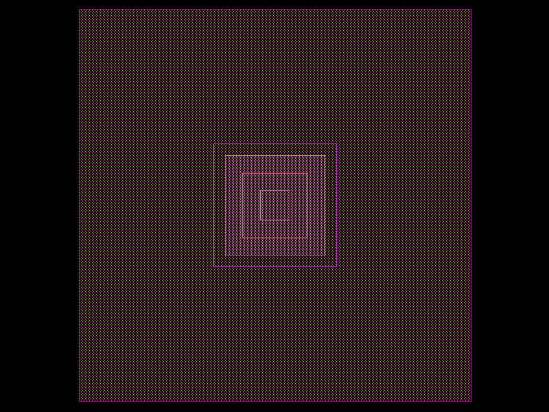
cap_mos#
- gf180mcu.cells.cap_mos(type='cap_nmos', lc=0.1, wc=0.1, volt='3.3V', deepnwell=False, pcmpgr=False, label=False, g_label='', sd_label='')[source]#
MOS capacitor (NMOS/PMOS varactor) matching Magic VLSI reference geometry.
Centered at origin. Gate = poly2 over lc × wc area; body = comp ring.
- Parameters:
type (str) – “cap_nmos” or “cap_pmos”.
lc (float) – Capacitor gate length (µm).
wc (float) – Capacitor gate width (µm).
volt (str) – “3.3V” or “6.0V”.
deepnwell (bool) – Unused (reserved).
pcmpgr (bool) – Unused (reserved).
label (bool) – Add metal1 labels.
g_label (str) – Gate label text.
sd_label (str) – Source/drain label text.
- Return type:
Component
import gf180mcu

c = gf180mcu._cells["cap_mos"](type='cap_nmos', lc=0.1, wc=0.1, volt='3.3V', deepnwell=False, pcmpgr=False, label=False, g_label='', sd_label='')
c = c.copy()
c.draw_ports()
c.plot()
(Source code, png, hires.png, pdf)

diode_dw2ps#
- gf180mcu.cells.diode_dw2ps(la=0.1, wa=0.1, cw=0.1, volt='3.3V', pcmpgr=False, label=False, p_label='', n_label='')[source]#
Draw DNWELL/Psub diode.
- Parameters:
la (float) – diffusion length (anode).
wa (float) – diffusion width (anode).
cw (float) – contact width (ring width for annular cathode).
volt (str) – operating voltage (“3.3V” or “5/6V”).
pcmpgr (bool) – use P+ Guard Ring.
label (bool) – add labels.
p_label (str) – p terminal label text.
n_label (str) – n terminal label text.
- Return type:
Component
import gf180mcu

c = gf180mcu._cells["diode_dw2ps"](la=0.1, wa=0.1, cw=0.1, volt='3.3V', pcmpgr=False, label=False, p_label='', n_label='')
c = c.copy()
c.draw_ports()
c.plot()
(Source code, png, hires.png, pdf)
diode_nd2ps#
- gf180mcu.cells.diode_nd2ps(la=0.45, wa=0.45, volt='3.3V', deepnwell=False, pcmpgr=False, label=False, p_label='', n_label='')[source]#
Draw N+/LVPWELL diode matching Magic VLSI geometry.
- Parameters:
la (float) – diffusion length (anode).
wa (float) – diffusion width (anode).
volt (str) – operating voltage (“3.3V” or “6.0V”).
deepnwell (bool) – use Deep NWELL device (not implemented).
pcmpgr (bool) – use P+ Guard Ring for DNWELL (not implemented).
label (bool) – add labels (not implemented).
p_label (str) – p terminal label.
n_label (str) – n terminal label.
- Return type:
Component
import gf180mcu

c = gf180mcu._cells["diode_nd2ps"](la=0.45, wa=0.45, volt='3.3V', deepnwell=False, pcmpgr=False, label=False, p_label='', n_label='')
c = c.copy()
c.draw_ports()
c.plot()
(Source code, png, hires.png, pdf)
diode_nw2ps#
- gf180mcu.cells.diode_nw2ps(la=0.1, wa=0.1, cw=0.1, volt='3.3V', label=False, p_label='', n_label='')[source]#
Draw 3.3V Nwell/Psub diode.
- Parameters:
la (float) – diffusion length (anode).
wa (float) – diffusion width (anode).
cw (float) – cathode width.
volt (str) – operating voltage (“3.3V” or “5/6V”).
label (bool) – add labels.
p_label (str) – p terminal label text.
n_label (str) – n terminal label text.
- Return type:
Component
import gf180mcu

c = gf180mcu._cells["diode_nw2ps"](la=0.1, wa=0.1, cw=0.1, volt='3.3V', label=False, p_label='', n_label='')
c = c.copy()
c.draw_ports()
c.plot()
(Source code, png, hires.png, pdf)

diode_pd2nw#
- gf180mcu.cells.diode_pd2nw(la=0.45, wa=0.45, volt='3.3V', deepnwell=False, pcmpgr=False, label=False, p_label='', n_label='')[source]#
Draw P+/Nwell diode matching Magic VLSI geometry.
- Parameters:
la (float) – diffusion length.
wa (float) – diffusion width.
volt (str) – operating voltage (“3.3V” or “6.0V”).
deepnwell (bool) – use Deep NWELL device (not implemented).
pcmpgr (bool) – use P+ Guard Ring for DNWELL (not implemented).
label (bool) – add labels (not implemented).
p_label (str) – p terminal label.
n_label (str) – n terminal label.
- Return type:
Component
import gf180mcu

c = gf180mcu._cells["diode_pd2nw"](la=0.45, wa=0.45, volt='3.3V', deepnwell=False, pcmpgr=False, label=False, p_label='', n_label='')
c = c.copy()
c.draw_ports()
c.plot()
(Source code, png, hires.png, pdf)

diode_pw2dw#
- gf180mcu.cells.diode_pw2dw(la=0.1, wa=0.1, cw=0.1, volt='3.3V', pcmpgr=False, label=False, p_label='', n_label='')[source]#
Draw LVPWELL/DNWELL diode.
- Parameters:
la (float) – diffusion length (anode).
wa (float) – diffusion width (anode).
cw (float) – cathode width.
volt (str) – operating voltage (“3.3V” or “5/6V”).
pcmpgr (bool) – use P+ Guard Ring.
label (bool) – add labels.
p_label (str) – p terminal label text.
n_label (str) – n terminal label text.
- Return type:
Component
import gf180mcu

c = gf180mcu._cells["diode_pw2dw"](la=0.1, wa=0.1, cw=0.1, volt='3.3V', pcmpgr=False, label=False, p_label='', n_label='')
c = c.copy()
c.draw_ports()
c.plot()
(Source code, png, hires.png, pdf)
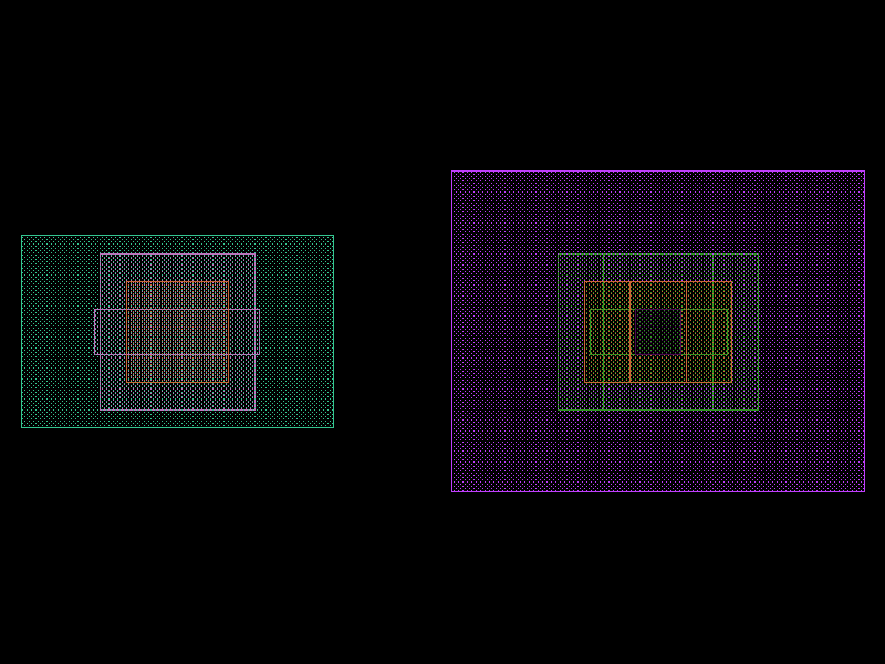
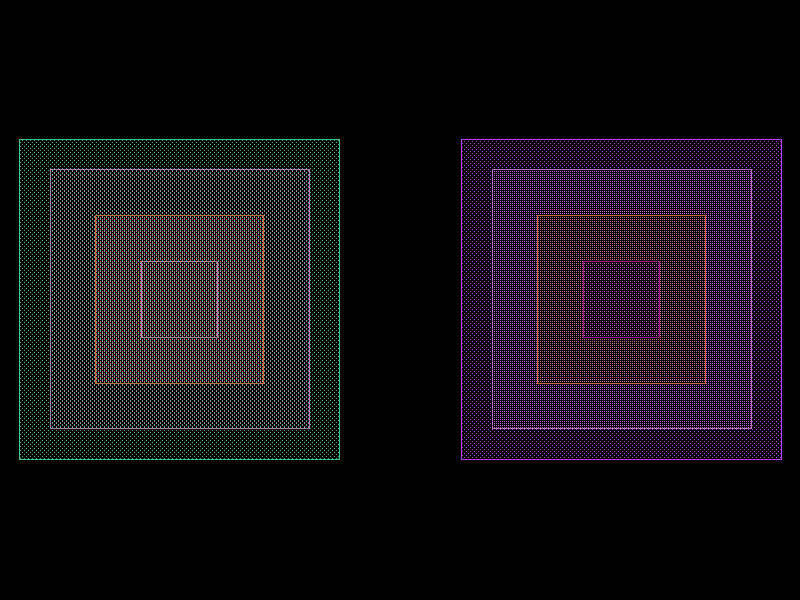
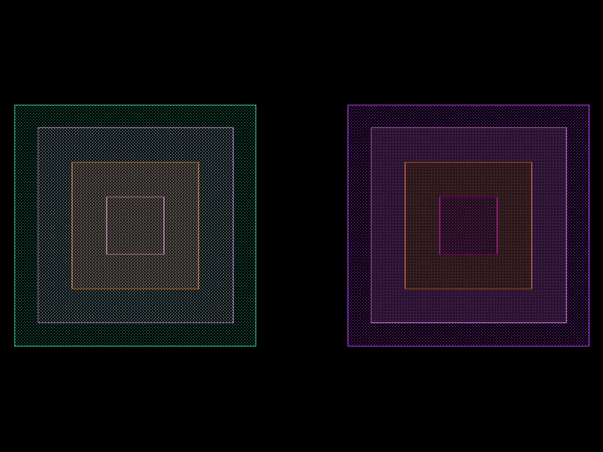
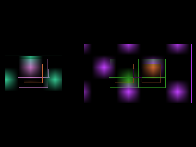
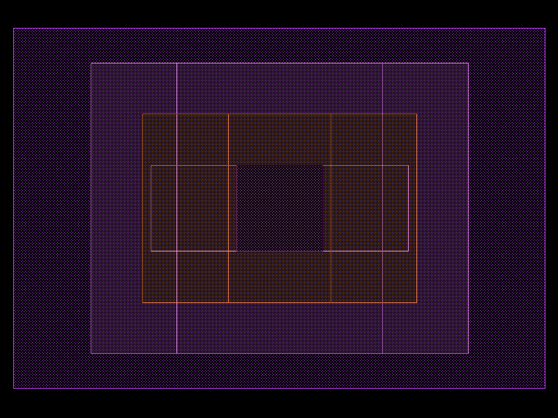
dn_rect#
- gf180mcu.cells.dn_rect(size=(4.0, 2.0), *, layer=<LAYER.dnwell: 47>, centered=False, port_type='electrical', port_orientations=(180, 90, 0, -90))#
Returns a rectangle.
- Parameters:
size (Size) – (tuple) Width and height of rectangle.
layer (LayerSpec) – Specific layer to put polygon geometry on.
centered (bool) – True sets center to (0, 0), False sets south-west to (0, 0).
port_type (str | None) – optical, electrical.
port_orientations (Ints | None) – list of port_orientations to add. None adds no ports.
- Return type:
Component
import gf180mcu

c = gf180mcu._cells["dn_rect"](size=(4, 2), layer='dnwell', centered=False, port_type='electrical', port_orientations=(180, 90, 0, -90))
c = c.copy()
c.draw_ports()
c.plot()
(Source code, png, hires.png, pdf)
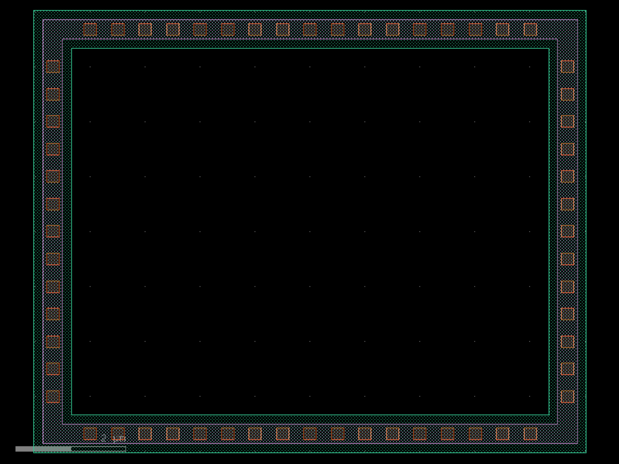
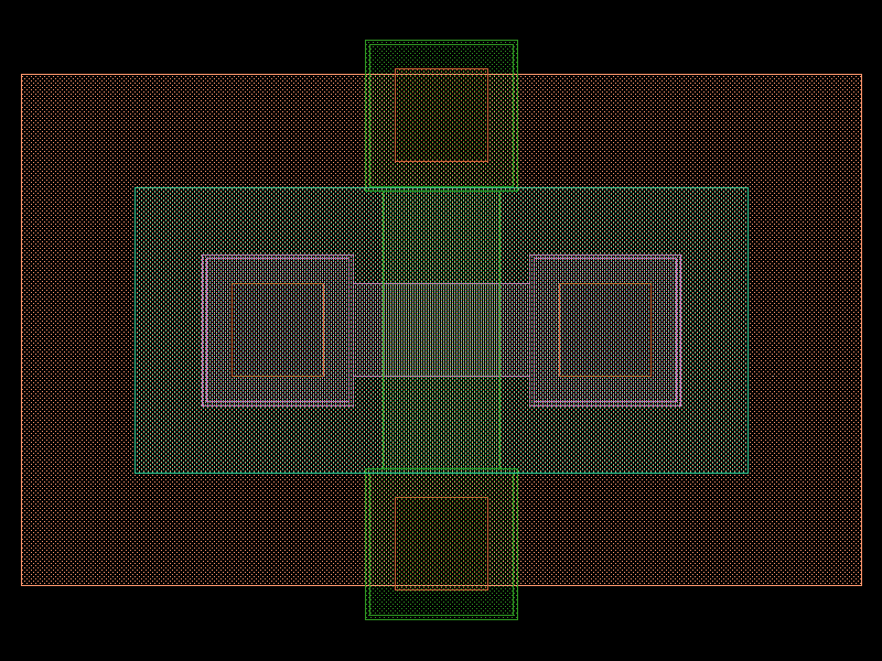
nfet#
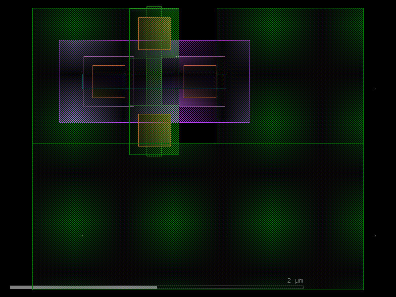
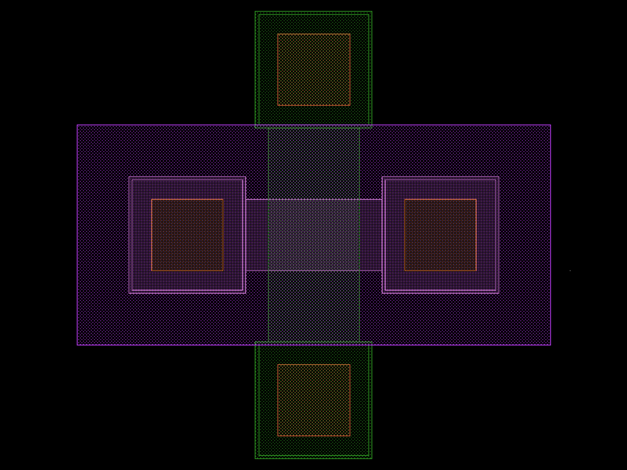
- gf180mcu.cells.nfet(l_gate=0.28, w_gate=0.22, sd_con_col=1, inter_sd_l=0.24, nf=1, grw=0.22, volt='3.3V', bulk='None', con_bet_fin=1, gate_con_pos='alternating', interdig=0, patt='', deepnwell=0, pcmpgr=0, label=False, sd_label=[], g_label=(), sub_label='', patt_label=False, dss=False, asym=False)[source]#
Return NFET transistor matching Magic VLSI geometry.
- Parameters:
l_gate (float) – gate length in microns.
w_gate (float) – gate width in microns.
sd_con_col (int) – number of source/drain contact columns.
inter_sd_l (float) – inter source/drain length.
nf (int) – number of gate fingers.
grw (float) – guard-ring width; set to 0 to disable the guard ring.
volt (str) – voltage rating (“3.3V”, “5.0V”, “6.0V”, “10.0V”).
bulk (str) – bulk connection option.
con_bet_fin (int) – contacts between fingers.
gate_con_pos (str) – gate contact position (“alternating”, “top”, “bottom”).
interdig (int) – interdigitated layout toggle.
patt (str) – gate pattern option.
deepnwell (int) – deep N-well toggle.
pcmpgr (int) – P-comp guard-ring toggle.
label (bool) – add text labels.
sd_label (Sequence[str] | None) – per-terminal source/drain label strings.
g_label (Sequence[str]) – gate label strings.
sub_label (str) – substrate label string.
patt_label (bool) – enable pattern labels.
dss (bool) – drain-side symmetric spacing.
asym (bool) – asymmetric layout.
- Return type:
Component
import gf180mcu

c = gf180mcu._cells["nfet"](l_gate=0.28, w_gate=0.22, sd_con_col=1, inter_sd_l=0.24, nf=1, grw=0.22, volt='3.3V', bulk='None', con_bet_fin=1, gate_con_pos='alternating', interdig=0, patt='', deepnwell=0, pcmpgr=0, label=False, g_label=(), sub_label='', patt_label=False, dss=False, asym=False)
c = c.copy()
c.draw_ports()
c.plot()
(Source code, png, hires.png, pdf)

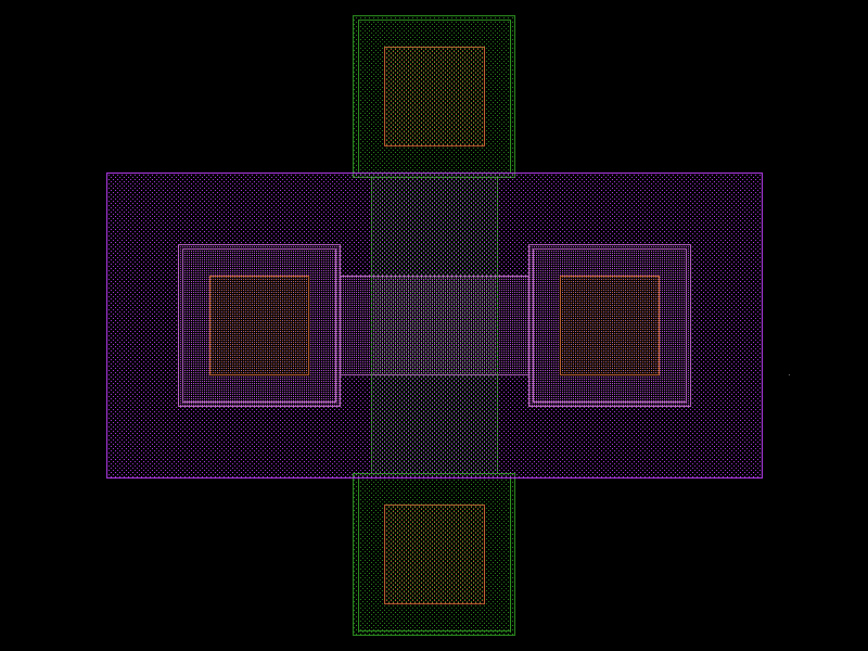
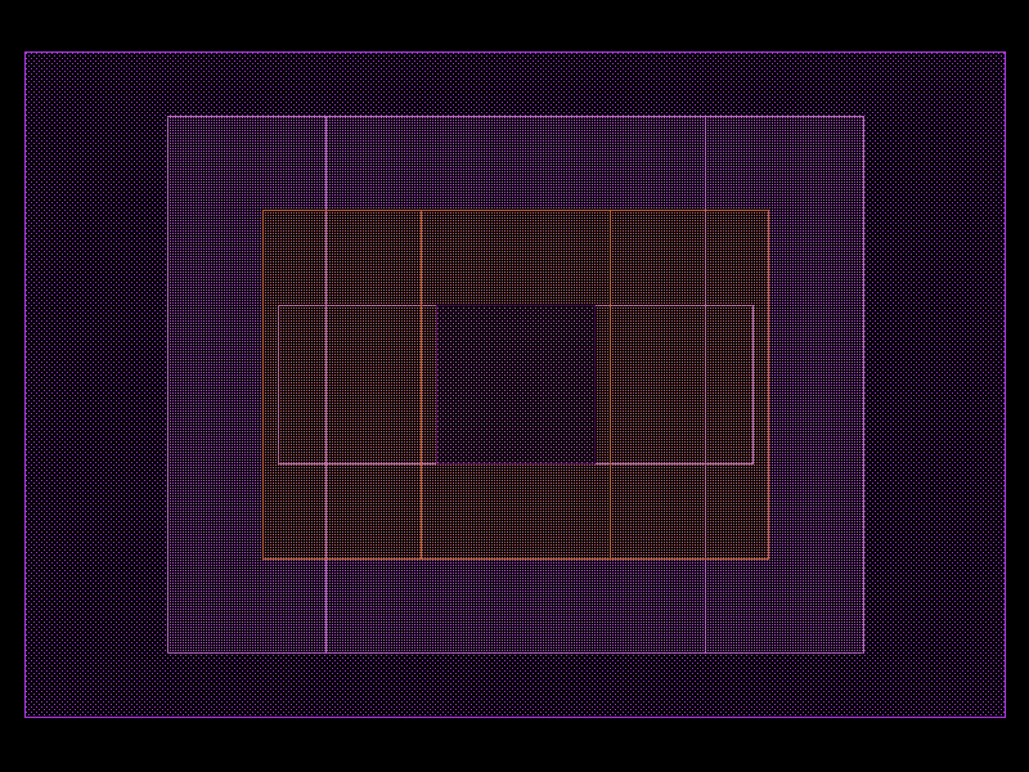
nfet_06v0_nvt#
- gf180mcu.cells.nfet_06v0_nvt(l_gate=1.8, w_gate=0.8, sd_con_col=1, inter_sd_l=0.24, nf=1, grw=0.22, bulk='None', con_bet_fin=1, gate_con_pos='alternating', interdig=0, patt='', label=False, sd_label=[], g_label=[], sub_label='', patt_label=False)[source]#
Return Native NFET 6V transistor matching Magic VLSI geometry.
- Parameters:
l_gate (float) – gate length in microns.
w_gate (float) – gate width in microns.
sd_con_col (int) – number of source/drain contact columns.
inter_sd_l (float) – inter source/drain length.
nf (int) – number of gate fingers.
grw (float) – guard-ring width; set to 0 to disable the guard ring.
bulk – bulk connection option.
con_bet_fin (int) – contacts between fingers.
gate_con_pos – gate contact position (“alternating”, “top”, “bottom”).
interdig (int) – interdigitated layout toggle.
patt – gate pattern option.
label (bool) – add text labels.
sd_label (Sequence[str] | None) – per-terminal source/drain label strings.
g_label (str) – gate label strings.
sub_label (str) – substrate label string.
patt_label (bool) – enable pattern labels.
- Return type:
Component
import gf180mcu

c = gf180mcu._cells["nfet_06v0_nvt"](l_gate=1.8, w_gate=0.8, sd_con_col=1, inter_sd_l=0.24, nf=1, grw=0.22, bulk='None', con_bet_fin=1, gate_con_pos='alternating', interdig=0, patt='', label=False, sub_label='', patt_label=False)
c = c.copy()
c.draw_ports()
c.plot()
(Source code, png, hires.png, pdf)
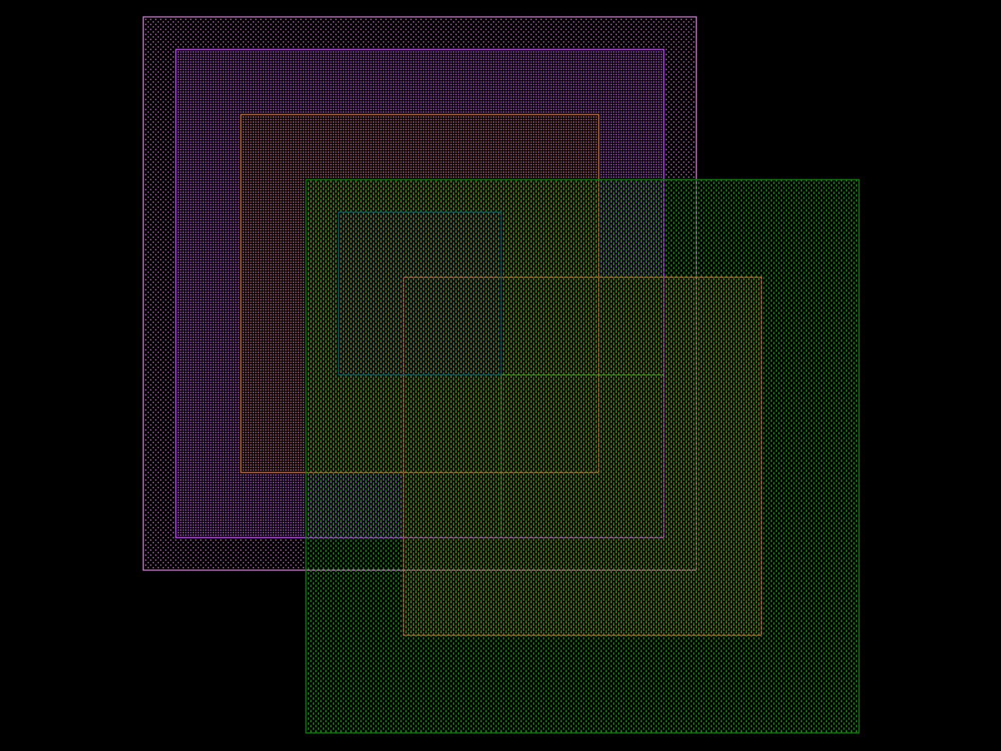
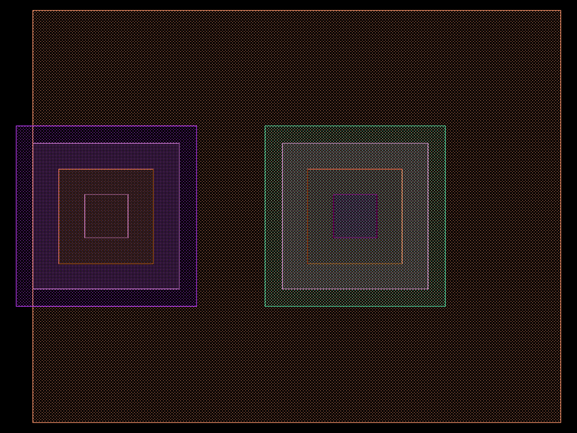
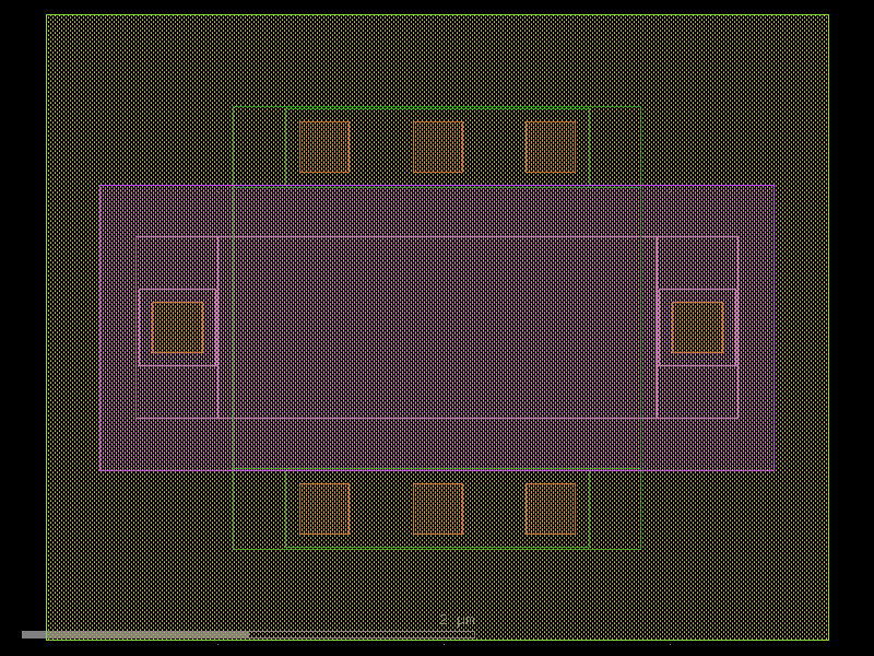
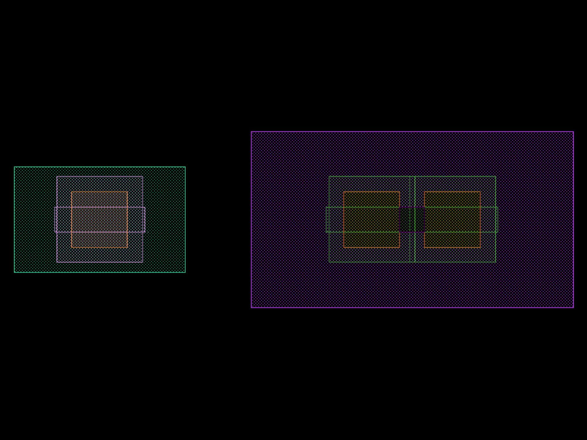
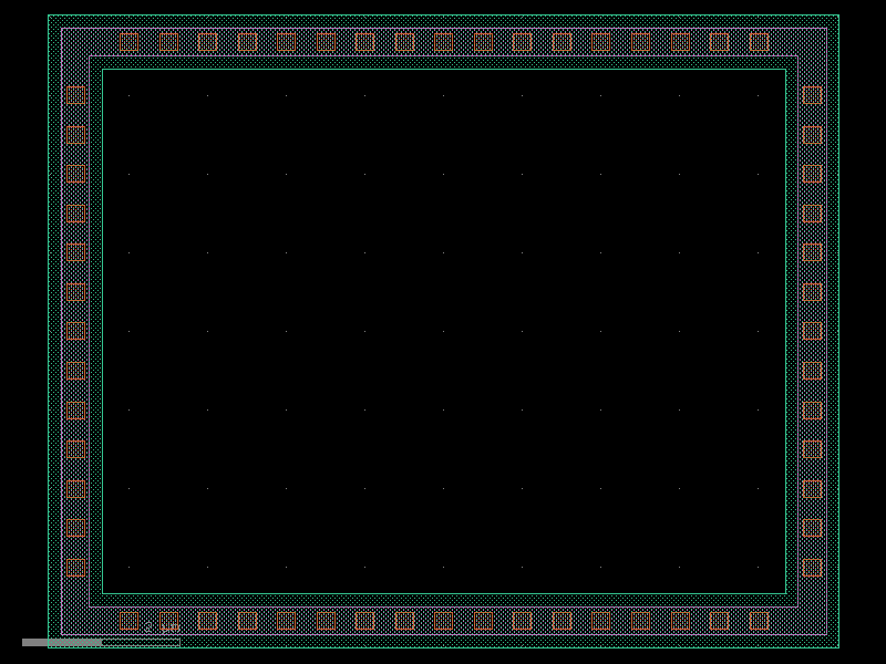
pcmpgr_gen#
- gf180mcu.cells.pcmpgr_gen(dn_rect=functools.partial(<function rectangle>, layer=<LAYER.dnwell: 47>), grw=0.36)[source]#
Return deepnwell guardring.
- Parameters:
dn_rect – deepnwell polygon.
grw (float) – guardring width.
- Return type:
Component
import gf180mcu

c = gf180mcu._cells["pcmpgr_gen"](grw=0.36)
c = c.copy()
c.draw_ports()
c.plot()
(Source code, png, hires.png, pdf)
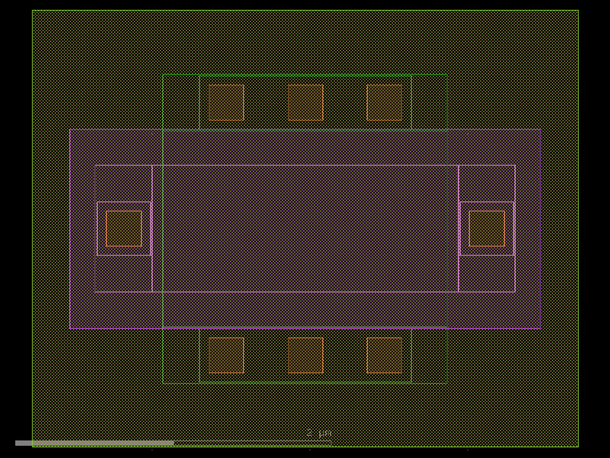
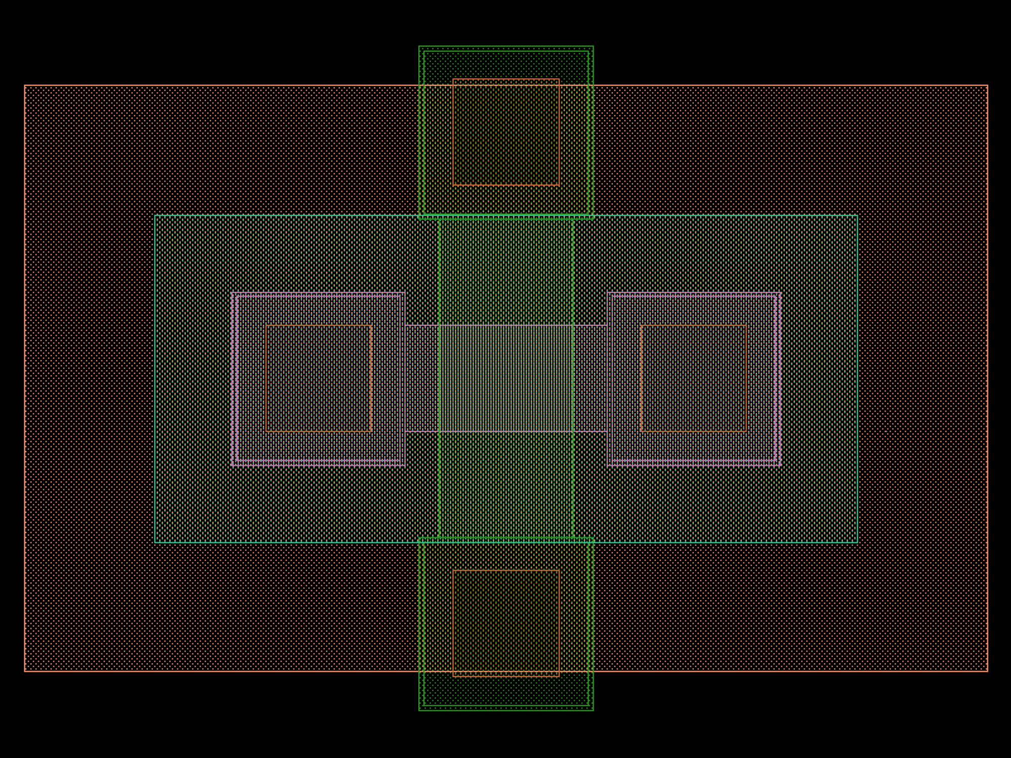
pfet#
- gf180mcu.cells.pfet(l_gate=0.28, w_gate=0.22, sd_con_col=1, inter_sd_l=0.24, nf=1, grw=0.22, volt='3.3V', bulk='None', con_bet_fin=1, gate_con_pos='alternating', interdig=0, patt='', deepnwell=0, pcmpgr=0, label=False, sd_label=(), g_label=(), sub_label='', patt_label=False, dss=False, asym=False)[source]#
Return PFET transistor matching Magic VLSI geometry.
- Parameters:
l_gate (float) – gate length in microns.
w_gate (float) – gate width in microns.
sd_con_col (int) – number of source/drain contact columns.
inter_sd_l (float) – inter source/drain length.
nf (int) – number of gate fingers.
grw (float) – guard-ring width; set to 0 to disable the guard ring.
volt (str) – voltage rating (“3.3V”, “5.0V”, “6.0V”, “10.0V”).
bulk (str) – bulk connection option.
con_bet_fin (int) – contacts between fingers.
gate_con_pos (str) – gate contact position (“alternating”, “top”, “bottom”).
interdig (int) – interdigitated layout toggle.
patt (str) – gate pattern option.
deepnwell (int) – deep N-well toggle.
pcmpgr (int) – P-comp guard-ring toggle.
label (bool) – add text labels.
sd_label (Sequence[str] | None) – per-terminal source/drain label strings.
g_label (Sequence[str]) – gate label strings.
sub_label (str) – substrate label string.
patt_label (bool) – enable pattern labels.
dss (bool) – drain-side symmetric spacing.
asym (bool) – asymmetric layout.
- Return type:
Component
import gf180mcu

c = gf180mcu._cells["pfet"](l_gate=0.28, w_gate=0.22, sd_con_col=1, inter_sd_l=0.24, nf=1, grw=0.22, volt='3.3V', bulk='None', con_bet_fin=1, gate_con_pos='alternating', interdig=0, patt='', deepnwell=0, pcmpgr=0, label=False, sd_label=(), g_label=(), sub_label='', patt_label=False, dss=False, asym=False)
c = c.copy()
c.draw_ports()
c.plot()
(Source code, png, hires.png, pdf)

res#
- gf180mcu.cells.res(l_res=0.1, w_res=0.1, res_type='rm1', label=False, r0_label='', r1_label='')[source]#
Returns a resistor component matching Magic VLSI geometry.
All layouts are centered at the origin with length along Y and width along X.
- Parameters:
l_res (float) – resistor length.
w_res (float) – resistor width.
res_type (str) – resistor variant.
label (bool) – whether to generate labels.
r0_label (str) – label for terminal 0.
r1_label (str) – label for terminal 1.
- Return type:
Component
import gf180mcu

c = gf180mcu._cells["res"](l_res=0.1, w_res=0.1, res_type='rm1', label=False, r0_label='', r1_label='')
c = c.copy()
c.draw_ports()
c.plot()
(Source code, png, hires.png, pdf)
sc_diode#
- gf180mcu.cells.sc_diode(la=0.1, wa=0.1, cw=0.1, m=1, pcmpgr=False, label=False, p_label='', n_label='')[source]#
Draw Schottky diode with interdigitated cathode/anode array.
- Parameters:
la (float) – diffusion length (anode).
wa (float) – diffusion width (anode).
cw (float) – cathode width.
m (int) – number of anode fingers.
pcmpgr (bool) – use P+ Guard Ring.
label (bool) – add labels.
p_label (str) – p terminal label text.
n_label (str) – n terminal label text.
- Return type:
Component
import gf180mcu

c = gf180mcu._cells["sc_diode"](la=0.1, wa=0.1, cw=0.1, m=1, pcmpgr=False, label=False, p_label='', n_label='')
c = c.copy()
c.draw_ports()
c.plot()
(Source code, png, hires.png, pdf)

straight#
- gf180mcu.cells.straight(length=10, cross_section='metal1', width=None)[source]#
Returns a Straight waveguide.
- Parameters:
length (float) – straight length (um).
cross_section (CrossSection | str | dict[str, Any] | Callable[[...], CrossSection] | SymmetricalCrossSection | DCrossSection) – specification (CrossSection, string or dict).
width (float | None) – width of the waveguide. If None, it will use the width of the cross_section.
- Return type:
Component
import gf180mcu

c = gf180mcu._cells["straight"](length=10, cross_section='metal1')
c = c.copy()
c.draw_ports()
c.plot()
(Source code, png, hires.png, pdf)
via_generator#
- gf180mcu.cells.via_generator(x_range=(0, 1), y_range=(0, 1), via_size=(0.17, 0.17), via_layer=(66, 44), via_enclosure=(0.06, 0.06), via_spacing=(0.17, 0.17))[source]#
Return only vias withen the range xrange and yrange while enclosing by via_enclosure and set number of rows and number of columns according to ranges and via size and spacing.
- Parameters:
x_range (tuple[float, float]) – dx range.
y_range (tuple[float, float]) – dy range.
via_size (tuple[float, float]) – via size.
via_layer (tuple[int, int] | str | int | LayerEnum) – via layer.
via_enclosure (tuple[float, float]) – via enclosure.
via_spacing (tuple[float, float]) – via spacing.
- Return type:
Component
import gf180mcu

c = gf180mcu._cells["via_generator"](x_range=(0, 1), y_range=(0, 1), via_size=(0.17, 0.17), via_layer=(66, 44), via_enclosure=(0.06, 0.06), via_spacing=(0.17, 0.17))
c = c.copy()
c.draw_ports()
c.plot()
(Source code, png, hires.png, pdf)

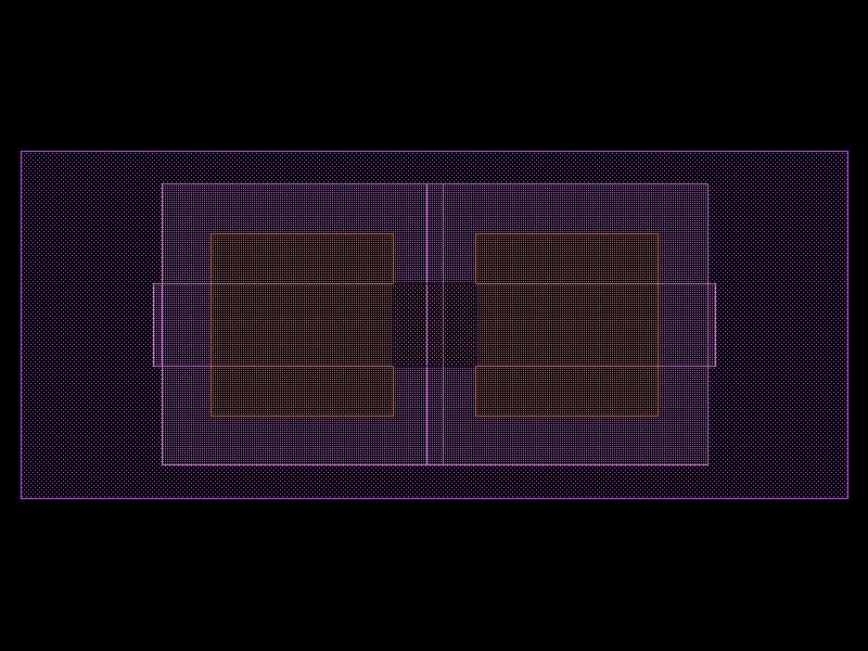
via_stack#
- gf180mcu.cells.via_stack(x_range=(0, 1), y_range=(0, 1), metal_level=1, con_size=(0.22, 0.22), con_enc=0.07, m_enc=0.06, con_spacing=(0.28, 0.28), via_size=(0.22, 0.22), via_spacing=(0.28, 0.28), via_enc=(0.06, 0.06), base_layer=<LAYER.metal1: 10>, **kwargs)[source]#
Returns a via stack withen the range xrange and yrange and expecting the base_layer to be drawen.
- Parameters:
x_range (tuple[float, float]) – dx range.
y_range (tuple[float, float]) – dy range.
metal_level (int) – metal level.
con_size (tuple[float, float]) – contact size.
con_enc (float) – contact enclosure.
m_enc (float) – metal enclosure.
con_spacing (tuple[float, float]) – contact spacing.
via_size (tuple[float, float]) – via size.
via_spacing (tuple[float, float]) – via spacing.
via_enc (tuple[float, float]) – via enclosure.
base_layer (tuple[int, int] | str | int | LayerEnum)
kwargs (Any)
- Return type:
Component
return via stack till the metal level indicated where : metal_level 1 : till m1 metal_level 2 : till m2 metal_level 3 : till m3 metal_level 4 : till m4 metal_level 5 : till m5 withen the range xrange and yrange and expecting the base_layer to be drawen
import gf180mcu

c = gf180mcu._cells["via_stack"](x_range=(0, 1), y_range=(0, 1), metal_level=1, con_size=(0.22, 0.22), con_enc=0.07, m_enc=0.06, con_spacing=(0.28, 0.28), via_size=(0.22, 0.22), via_spacing=(0.28, 0.28), via_enc=(0.06, 0.06), base_layer='metal1')
c = c.copy()
c.draw_ports()
c.plot()
(Source code, png, hires.png, pdf)

wire_corner#
- gf180mcu.cells.wire_corner(cross_section='metal2', width=None)[source]#
Returns 45 degrees electrical corner wire.
- Parameters:
cross_section (CrossSection | str | dict[str, Any] | Callable[[...], CrossSection] | SymmetricalCrossSection | DCrossSection) – spec.
width (float | None) – optional width. Defaults to cross_section width.
- Return type:
Component
import gf180mcu

c = gf180mcu._cells["wire_corner"](cross_section='metal2')
c = c.copy()
c.draw_ports()
c.plot()
(Source code, png, hires.png, pdf)
wire_corner45#
- gf180mcu.cells.wire_corner45(cross_section='metal2', radius=10, width=None, layer=None, with_corner90_ports=True)[source]#
Returns 90 degrees electrical corner wire.
- Parameters:
cross_section (CrossSection | str | dict[str, Any] | Callable[[...], CrossSection] | SymmetricalCrossSection | DCrossSection) – spec.
radius (float) – ignored.
width (float | None) – optional width. Defaults to cross_section width.
layer (tuple[int, int] | str | int | LayerEnum | None) – ignored.
with_corner90_ports (bool) – if True, adds ports at 90 degrees.
- Return type:
Component
import gf180mcu

c = gf180mcu._cells["wire_corner45"](cross_section='metal2', radius=10, with_corner90_ports=True)
c = c.copy()
c.draw_ports()
c.plot()
(Source code, png, hires.png, pdf)