Cells
Parametric Cells (PCells)
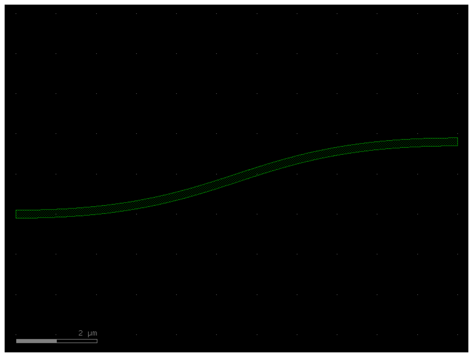
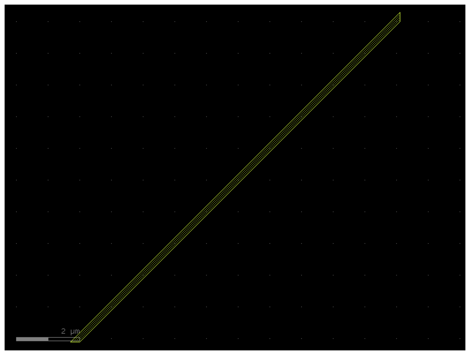
bend
Regular degree euler bend.
Parameters:
| Name | Type | Description | Default |
|---|---|---|---|
radius
|
float | None
|
None. |
None
|
angle
|
float
|
90. |
90
|
width
|
float | None
|
None. |
None
|
cross_section
|
CrossSectionSpec
|
"metal1". |
'metal1'
|

import gf180mcu

gf180mcu.PDK.activate()
c = gf180mcu._cells["bend"](angle=90, cross_section='metal1')
c.draw_ports()
c.plot()
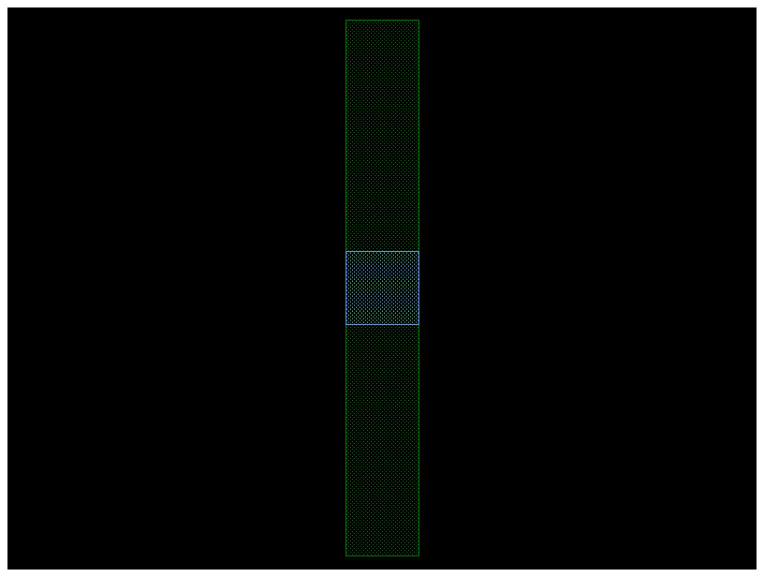
bend_s
Return S bend with bezier curve.
stores min_bend_radius property in self.info['min_bend_radius'] min_bend_radius depends on height and length
Parameters:
| Name | Type | Description | Default |
|---|---|---|---|
size
|
Size
|
in x and y direction. |
(11, 1.8)
|
cross_section
|
CrossSectionSpec
|
spec. |
'metal1'
|
width
|
float | None
|
width of the waveguide. If None, it will use the width of the cross_section. |
None
|
import gf180mcu

gf180mcu.PDK.activate()
c = gf180mcu._cells["bend_s"](size=(11, 1.8), cross_section='metal1')
c.draw_ports()
c.plot()
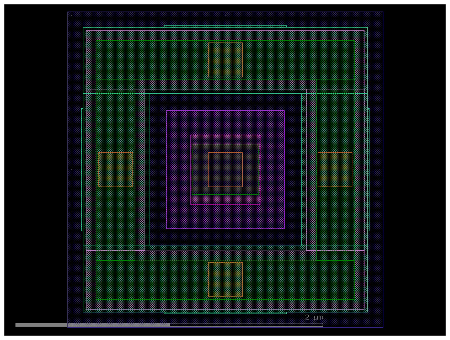
cap_mim
MIM capacitor pcell matching Magic VLSI geometry exactly.
Implements gf180mcu::cap_mim_2p0fF_draw / cap_device from Magic generators. Uses MIM-A (metal2/metal3) stack with fusetop cap plate.
cap_mim(mim_option='A', metal_level='M4', lc=5, wc=5, label=False, top_label='', bot_label='')
Return MIM capacitor matching Magic VLSI geometry.
Parameters:
| Name | Type | Description | Default |
|---|---|---|---|
mim_option
|
str
|
MIM-A or MIM-B (only A currently matched). |
'A'
|
metal_level
|
str
|
metal level (ignored for MIM-A). |
'M4'
|
lc
|
float
|
cap length (Magic 'l'). |
5
|
wc
|
float
|
cap width (Magic 'w'). |
5
|
label
|
bool
|
whether to add labels. |
False
|
top_label
|
str
|
top label text. |
''
|
bot_label
|
str
|
bottom label text. |
''
|
import gf180mcu

gf180mcu.PDK.activate()
c = gf180mcu._cells["cap_mim"](mim_option='A', metal_level='M4', lc=5, wc=5, label=False, top_label='', bot_label='')
c.draw_ports()
c.plot()
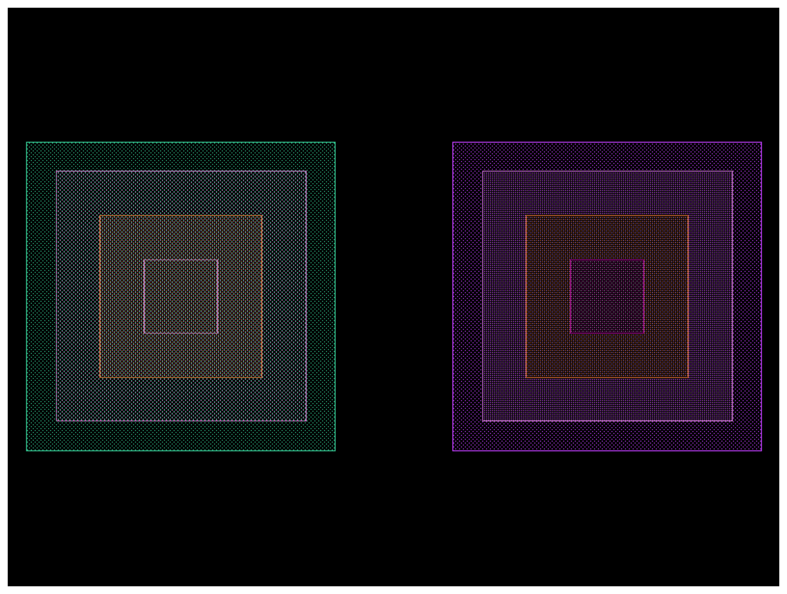
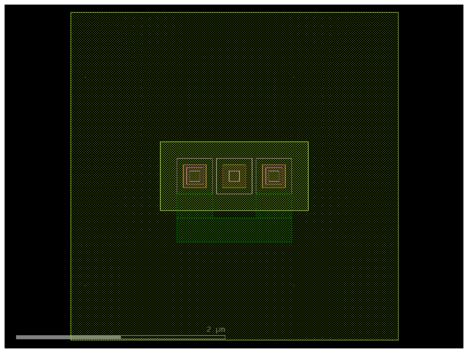
cap_mos
GF180MCU MOS capacitor parametric cells.
Geometry is derived from the open_pdks Magic VLSI generators
gf180mcu::nmoscap_3p3_draw / nmoscap_6p0_draw → gf180mcu::mos_draw
The MOS capacitor is a MOSFET varactor
- Gate terminal : poly2 over the lc × wc gate area
- Body terminal : nsd comp strips adjacent to the gate + outer lvpwell guard ring
All geometry is centered at origin and snapped to a 5 nm grid.
Magic ruleset (painted coordinates): contact_size = 0.23 → 0.22 CIF cut (half-cut = 0.11) diff_surround = 0.065 → 0.07 CIF active surround poly_surround = 0.065 → 0.07 CIF metal_surround = 0.055 → 0.06 CIF gate_to_diffcont = 0.26 gate_to_polycont = 0.28 metal_spacing = 0.23
cap_mos(type='cap_nmos', lc=0.1, wc=0.1, volt='3.3V', deepnwell=False, pcmpgr=False, label=False, g_label='', sd_label='')
MOS capacitor (NMOS/PMOS varactor) matching Magic VLSI reference geometry.
Centered at origin. Gate = poly2 over lc × wc area; body = comp ring.
Parameters:
| Name | Type | Description | Default |
|---|---|---|---|
type
|
str
|
"cap_nmos" or "cap_pmos". |
'cap_nmos'
|
lc
|
float
|
Capacitor gate length (µm). |
0.1
|
wc
|
float
|
Capacitor gate width (µm). |
0.1
|
volt
|
str
|
"3.3V" or "6.0V". |
'3.3V'
|
deepnwell
|
bool
|
Unused (reserved). |
False
|
pcmpgr
|
bool
|
Unused (reserved). |
False
|
label
|
bool
|
Add metal1 labels. |
False
|
g_label
|
str
|
Gate label text. |
''
|
sd_label
|
str
|
Source/drain label text. |
''
|
import gf180mcu

gf180mcu.PDK.activate()
c = gf180mcu._cells["cap_mos"](type='cap_nmos', lc=0.1, wc=0.1, volt='3.3V', deepnwell=False, pcmpgr=False, label=False, g_label='', sd_label='')
c.draw_ports()
c.plot()
diode_dw2ps
Draw DNWELL/Psub diode.
Parameters:
| Name | Type | Description | Default |
|---|---|---|---|
la
|
float
|
diffusion length (anode). |
0.1
|
wa
|
float
|
diffusion width (anode). |
0.1
|
cw
|
float
|
contact width (ring width for annular cathode). |
0.1
|
volt
|
str
|
operating voltage ("3.3V" or "⅚V"). |
'3.3V'
|
pcmpgr
|
bool
|
use P+ Guard Ring. |
False
|
label
|
bool
|
add labels. |
False
|
p_label
|
str
|
p terminal label text. |
''
|
n_label
|
str
|
n terminal label text. |
''
|
import gf180mcu

gf180mcu.PDK.activate()
c = gf180mcu._cells["diode_dw2ps"](la=0.1, wa=0.1, cw=0.1, volt='3.3V', pcmpgr=False, label=False, p_label='', n_label='')
c.draw_ports()
c.plot()
diode_nd2ps
Draw N+/LVPWELL diode matching Magic VLSI geometry.
Parameters:
| Name | Type | Description | Default |
|---|---|---|---|
la
|
float
|
diffusion length (anode). |
0.45
|
wa
|
float
|
diffusion width (anode). |
0.45
|
volt
|
str
|
operating voltage ("3.3V" or "6.0V"). |
'3.3V'
|
deepnwell
|
bool
|
use Deep NWELL device (not implemented). |
False
|
pcmpgr
|
bool
|
use P+ Guard Ring for DNWELL (not implemented). |
False
|
label
|
bool
|
add labels (not implemented). |
False
|
p_label
|
str
|
p terminal label. |
''
|
n_label
|
str
|
n terminal label. |
''
|
import gf180mcu

gf180mcu.PDK.activate()
c = gf180mcu._cells["diode_nd2ps"](la=0.45, wa=0.45, volt='3.3V', deepnwell=False, pcmpgr=False, label=False, p_label='', n_label='')
c.draw_ports()
c.plot()
diode_nw2ps
Draw 3.3V Nwell/Psub diode.
Parameters:
| Name | Type | Description | Default |
|---|---|---|---|
la
|
float
|
diffusion length (anode). |
0.1
|
wa
|
float
|
diffusion width (anode). |
0.1
|
cw
|
float
|
cathode width. |
0.1
|
volt
|
str
|
operating voltage ("3.3V" or "⅚V"). |
'3.3V'
|
label
|
bool
|
add labels. |
False
|
p_label
|
str
|
p terminal label text. |
''
|
n_label
|
str
|
n terminal label text. |
''
|
import gf180mcu

gf180mcu.PDK.activate()
c = gf180mcu._cells["diode_nw2ps"](la=0.1, wa=0.1, cw=0.1, volt='3.3V', label=False, p_label='', n_label='')
c.draw_ports()
c.plot()
diode_pd2nw
Draw P+/Nwell diode matching Magic VLSI geometry.
Parameters:
| Name | Type | Description | Default |
|---|---|---|---|
la
|
float
|
diffusion length. |
0.45
|
wa
|
float
|
diffusion width. |
0.45
|
volt
|
str
|
operating voltage ("3.3V" or "6.0V"). |
'3.3V'
|
deepnwell
|
bool
|
use Deep NWELL device (not implemented). |
False
|
pcmpgr
|
bool
|
use P+ Guard Ring for DNWELL (not implemented). |
False
|
label
|
bool
|
add labels (not implemented). |
False
|
p_label
|
str
|
p terminal label. |
''
|
n_label
|
str
|
n terminal label. |
''
|
import gf180mcu

gf180mcu.PDK.activate()
c = gf180mcu._cells["diode_pd2nw"](la=0.45, wa=0.45, volt='3.3V', deepnwell=False, pcmpgr=False, label=False, p_label='', n_label='')
c.draw_ports()
c.plot()
diode_pw2dw
Draw LVPWELL/DNWELL diode.
Parameters:
| Name | Type | Description | Default |
|---|---|---|---|
la
|
float
|
diffusion length (anode). |
0.1
|
wa
|
float
|
diffusion width (anode). |
0.1
|
cw
|
float
|
cathode width. |
0.1
|
volt
|
str
|
operating voltage ("3.3V" or "⅚V"). |
'3.3V'
|
pcmpgr
|
bool
|
use P+ Guard Ring. |
False
|
label
|
bool
|
add labels. |
False
|
p_label
|
str
|
p terminal label text. |
''
|
n_label
|
str
|
n terminal label text. |
''
|
import gf180mcu

gf180mcu.PDK.activate()
c = gf180mcu._cells["diode_pw2dw"](la=0.1, wa=0.1, cw=0.1, volt='3.3V', pcmpgr=False, label=False, p_label='', n_label='')
c.draw_ports()
c.plot()
dn_rect

import gf180mcu

gf180mcu.PDK.activate()
c = gf180mcu._cells["dn_rect"](size=(4, 2), layer='dnwell', centered=False, port_type='electrical', port_orientations=(180, 90, 0, -90))
c.draw_ports()
c.plot()
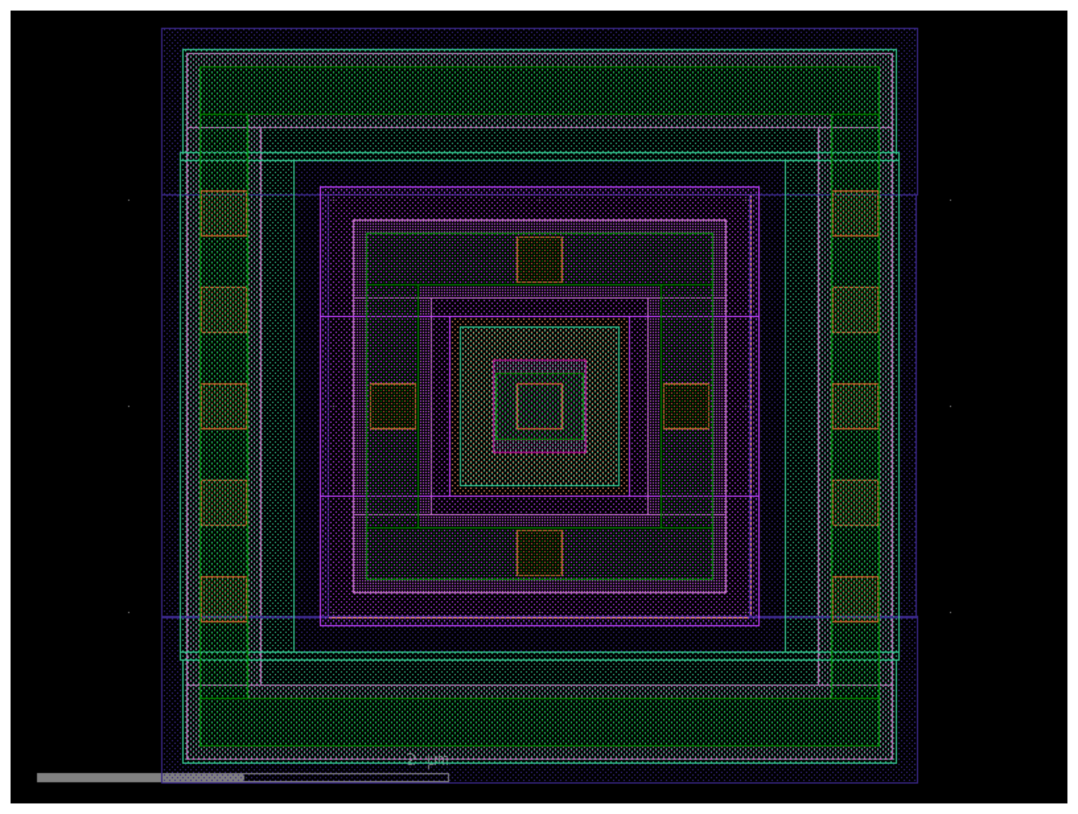
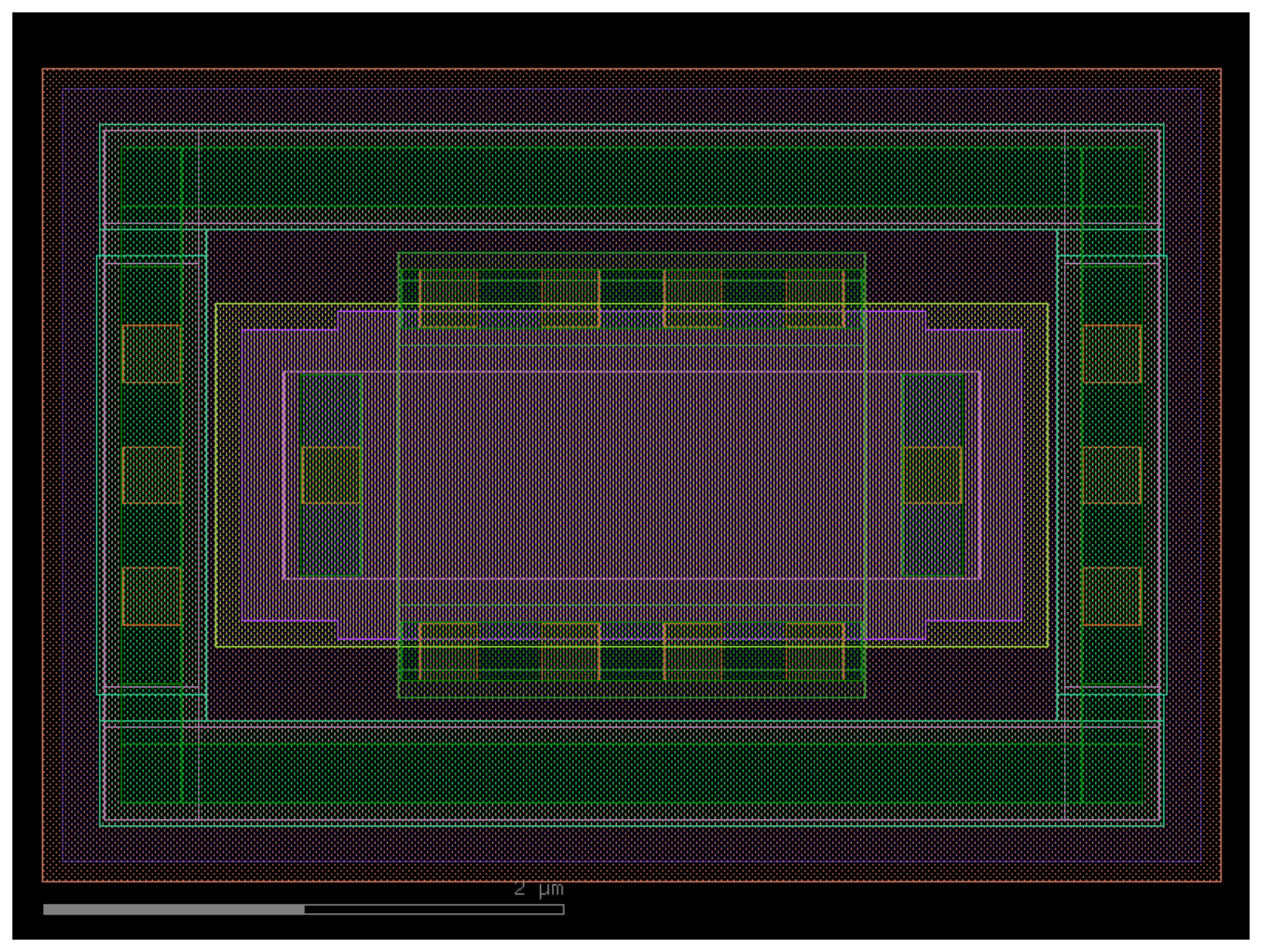
nfet
Return NFET transistor matching Magic VLSI geometry.
Parameters:
| Name | Type | Description | Default |
|---|---|---|---|
l_gate
|
float
|
gate length in microns. |
0.28
|
w_gate
|
float
|
gate width in microns. |
0.22
|
sd_con_col
|
int
|
number of source/drain contact columns. |
1
|
inter_sd_l
|
float
|
inter source/drain length. |
0.24
|
nf
|
int
|
number of gate fingers. |
1
|
grw
|
float
|
guard-ring width; set to 0 to disable the guard ring. |
0.22
|
volt
|
str
|
voltage rating ("3.3V", "5.0V", "6.0V", "10.0V"). |
'3.3V'
|
bulk
|
str
|
bulk connection option. |
'None'
|
con_bet_fin
|
int
|
contacts between fingers. |
1
|
gate_con_pos
|
str
|
gate contact position ("alternating", "top", "bottom"). |
'alternating'
|
interdig
|
int
|
interdigitated layout toggle. |
0
|
patt
|
str
|
gate pattern option. |
''
|
deepnwell
|
int
|
deep N-well toggle. |
0
|
pcmpgr
|
int
|
P-comp guard-ring toggle. |
0
|
label
|
bool
|
add text labels. |
False
|
sd_label
|
Strs | None
|
per-terminal source/drain label strings. |
[]
|
g_label
|
Strs
|
gate label strings. |
()
|
sub_label
|
str
|
substrate label string. |
''
|
patt_label
|
bool
|
enable pattern labels. |
False
|
dss
|
bool
|
drain-side symmetric spacing. |
False
|
asym
|
bool
|
asymmetric layout. |
False
|
import gf180mcu

gf180mcu.PDK.activate()
c = gf180mcu._cells["nfet"](l_gate=0.28, w_gate=0.22, sd_con_col=1, inter_sd_l=0.24, nf=1, grw=0.22, volt='3.3V', bulk='None', con_bet_fin=1, gate_con_pos='alternating', interdig=0, patt='', deepnwell=0, pcmpgr=0, label=False, g_label=(), sub_label='', patt_label=False, dss=False, asym=False)
c.draw_ports()
c.plot()
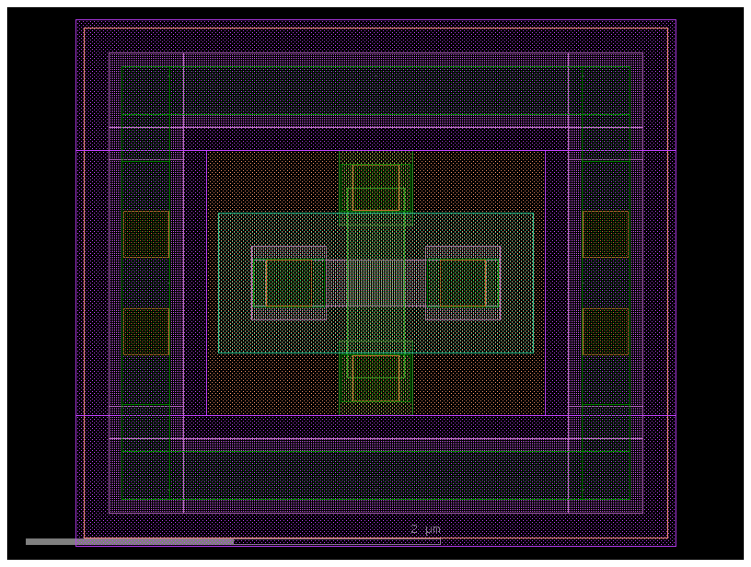
nfet_06v0_nvt
Return Native NFET 6V transistor matching Magic VLSI geometry.
Parameters:
| Name | Type | Description | Default |
|---|---|---|---|
l_gate
|
float
|
gate length in microns. |
1.8
|
w_gate
|
float
|
gate width in microns. |
0.8
|
sd_con_col
|
int
|
number of source/drain contact columns. |
1
|
inter_sd_l
|
float
|
inter source/drain length. |
0.24
|
nf
|
int
|
number of gate fingers. |
1
|
grw
|
float
|
guard-ring width; set to 0 to disable the guard ring. |
0.22
|
bulk
|
bulk connection option. |
'None'
|
|
con_bet_fin
|
int
|
contacts between fingers. |
1
|
gate_con_pos
|
gate contact position ("alternating", "top", "bottom"). |
'alternating'
|
|
interdig
|
int
|
interdigitated layout toggle. |
0
|
patt
|
gate pattern option. |
''
|
|
label
|
bool
|
add text labels. |
False
|
sd_label
|
Strs | None
|
per-terminal source/drain label strings. |
[]
|
g_label
|
str
|
gate label strings. |
[]
|
sub_label
|
str
|
substrate label string. |
''
|
patt_label
|
bool
|
enable pattern labels. |
False
|
import gf180mcu

gf180mcu.PDK.activate()
c = gf180mcu._cells["nfet_06v0_nvt"](l_gate=1.8, w_gate=0.8, sd_con_col=1, inter_sd_l=0.24, nf=1, grw=0.22, bulk='None', con_bet_fin=1, gate_con_pos='alternating', interdig=0, patt='', label=False, sub_label='', patt_label=False)
c.draw_ports()
c.plot()
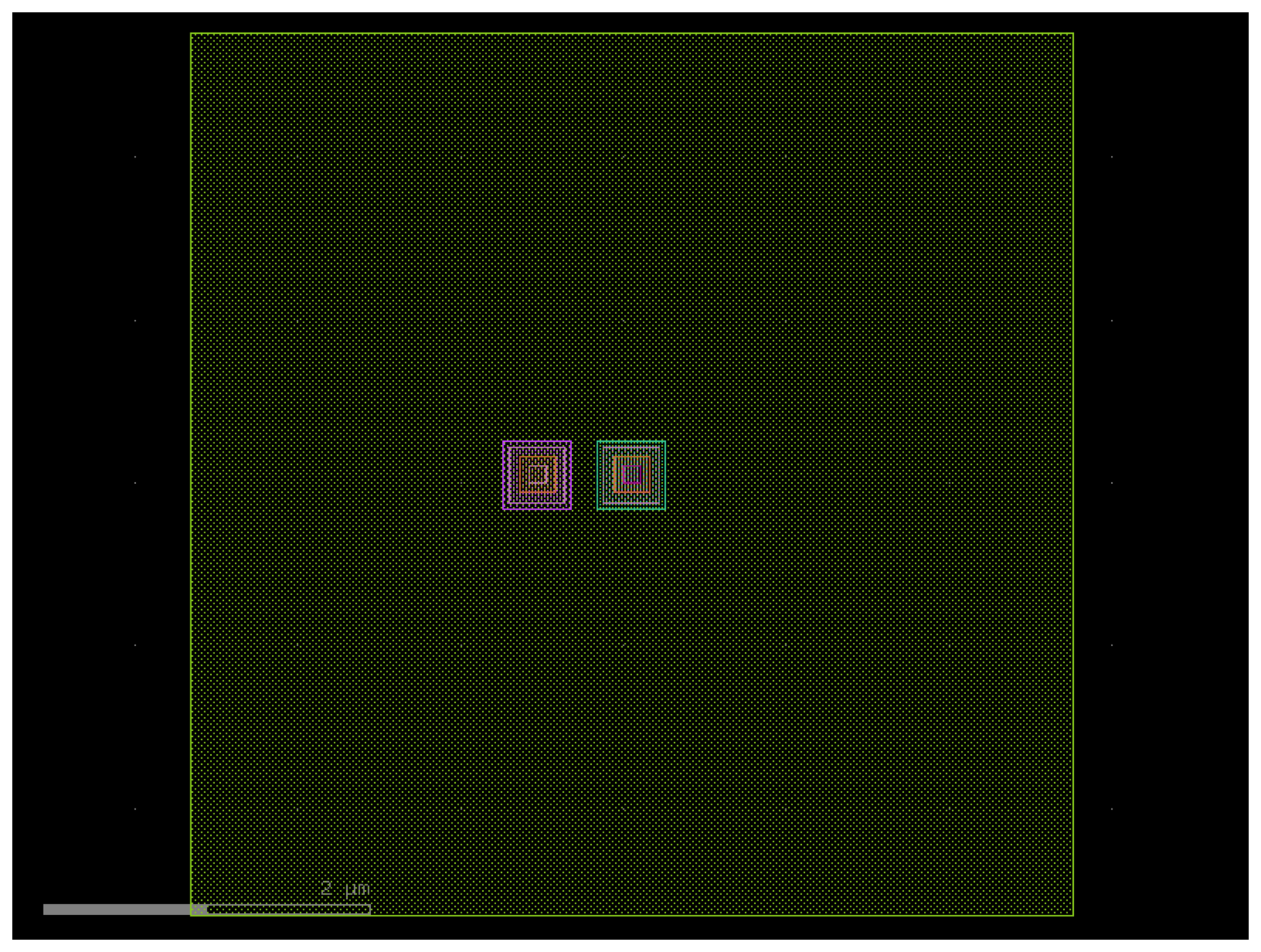
pcmpgr_gen
Return deepnwell guardring.
Parameters:
| Name | Type | Description | Default |
|---|---|---|---|
dn_rect
|
deepnwell polygon. |
required | |
grw
|
guardring width. |
required |
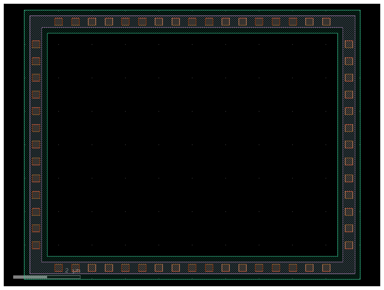
import gf180mcu

gf180mcu.PDK.activate()
c = gf180mcu._cells["pcmpgr_gen"](grw=0.36)
c.draw_ports()
c.plot()
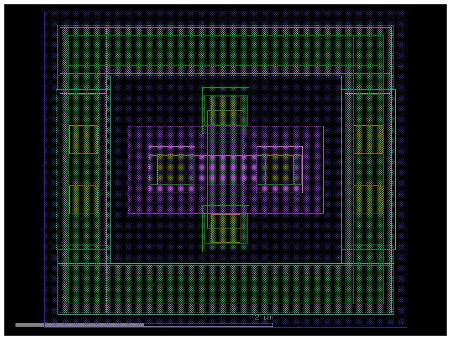
pfet
Return PFET transistor matching Magic VLSI geometry.
Parameters:
| Name | Type | Description | Default |
|---|---|---|---|
l_gate
|
float
|
gate length in microns. |
0.28
|
w_gate
|
float
|
gate width in microns. |
0.22
|
sd_con_col
|
int
|
number of source/drain contact columns. |
1
|
inter_sd_l
|
float
|
inter source/drain length. |
0.24
|
nf
|
int
|
number of gate fingers. |
1
|
grw
|
float
|
guard-ring width; set to 0 to disable the guard ring. |
0.22
|
volt
|
str
|
voltage rating ("3.3V", "5.0V", "6.0V", "10.0V"). |
'3.3V'
|
bulk
|
str
|
bulk connection option. |
'None'
|
con_bet_fin
|
int
|
contacts between fingers. |
1
|
gate_con_pos
|
str
|
gate contact position ("alternating", "top", "bottom"). |
'alternating'
|
interdig
|
int
|
interdigitated layout toggle. |
0
|
patt
|
str
|
gate pattern option. |
''
|
deepnwell
|
int
|
deep N-well toggle. |
0
|
pcmpgr
|
int
|
P-comp guard-ring toggle. |
0
|
label
|
bool
|
add text labels. |
False
|
sd_label
|
Strs | None
|
per-terminal source/drain label strings. |
()
|
g_label
|
Strs
|
gate label strings. |
()
|
sub_label
|
str
|
substrate label string. |
''
|
patt_label
|
bool
|
enable pattern labels. |
False
|
dss
|
bool
|
drain-side symmetric spacing. |
False
|
asym
|
bool
|
asymmetric layout. |
False
|
import gf180mcu

gf180mcu.PDK.activate()
c = gf180mcu._cells["pfet"](l_gate=0.28, w_gate=0.22, sd_con_col=1, inter_sd_l=0.24, nf=1, grw=0.22, volt='3.3V', bulk='None', con_bet_fin=1, gate_con_pos='alternating', interdig=0, patt='', deepnwell=0, pcmpgr=0, label=False, sd_label=(), g_label=(), sub_label='', patt_label=False, dss=False, asym=False)
c.draw_ports()
c.plot()
res
GF180MCU resistor pcells matching Magic VLSI geometry exactly.
All layouts are centered at the origin with length (l) along Y and width (w) along X, matching Magic's coordinate convention.
res(l_res=0.1, w_res=0.1, res_type='rm1', label=False, r0_label='', r1_label='')
Returns a resistor component matching Magic VLSI geometry.
All layouts are centered at the origin with length along Y and width along X.
Parameters:
| Name | Type | Description | Default |
|---|---|---|---|
l_res
|
float
|
resistor length. |
0.1
|
w_res
|
float
|
resistor width. |
0.1
|
res_type
|
str
|
resistor variant. |
'rm1'
|
label
|
bool
|
whether to generate labels. |
False
|
r0_label
|
str
|
label for terminal 0. |
''
|
r1_label
|
str
|
label for terminal 1. |
''
|
import gf180mcu

gf180mcu.PDK.activate()
c = gf180mcu._cells["res"](l_res=0.1, w_res=0.1, res_type='rm1', label=False, r0_label='', r1_label='')
c.draw_ports()
c.plot()
sc_diode
Draw Schottky diode with interdigitated cathode/anode array.
Parameters:
| Name | Type | Description | Default |
|---|---|---|---|
la
|
float
|
diffusion length (anode). |
0.1
|
wa
|
float
|
diffusion width (anode). |
0.1
|
cw
|
float
|
cathode width. |
0.1
|
m
|
int
|
number of anode fingers. |
1
|
pcmpgr
|
bool
|
use P+ Guard Ring. |
False
|
label
|
bool
|
add labels. |
False
|
p_label
|
str
|
p terminal label text. |
''
|
n_label
|
str
|
n terminal label text. |
''
|
import gf180mcu

gf180mcu.PDK.activate()
c = gf180mcu._cells["sc_diode"](la=0.1, wa=0.1, cw=0.1, m=1, pcmpgr=False, label=False, p_label='', n_label='')
c.draw_ports()
c.plot()
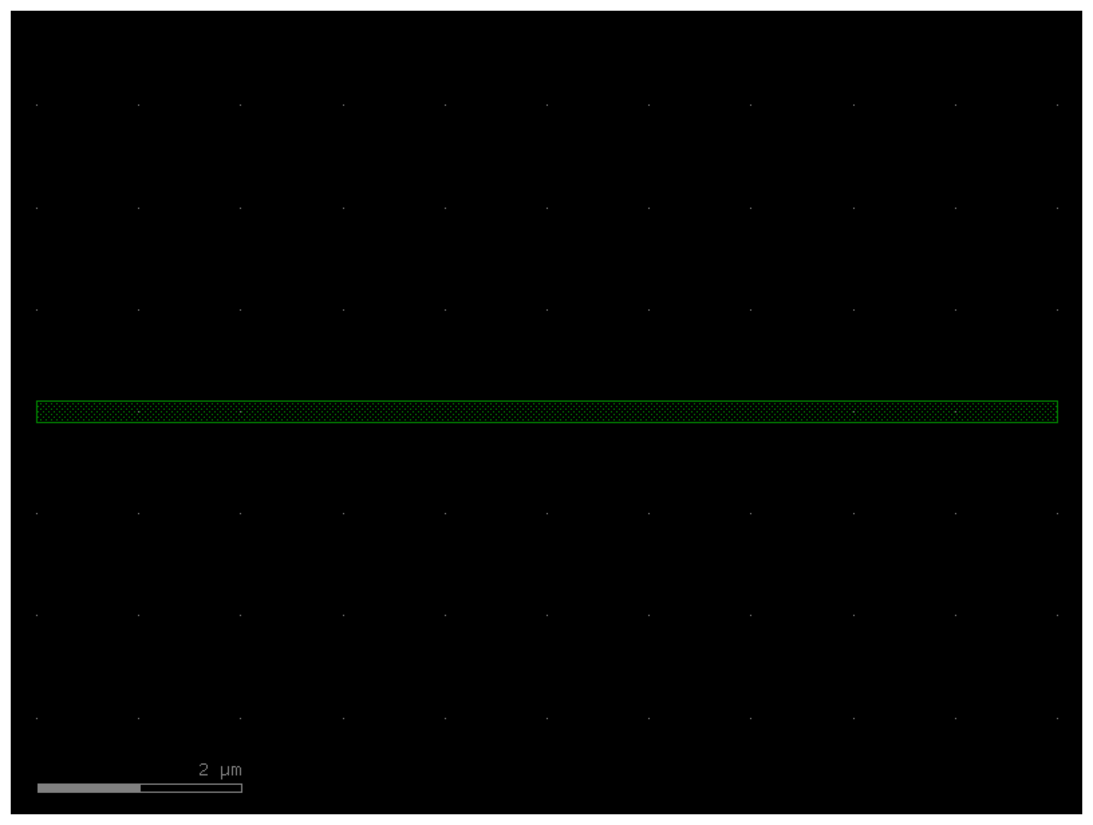
straight
Returns a Straight waveguide.
Parameters:
| Name | Type | Description | Default |
|---|---|---|---|
length
|
float
|
straight length (um). |
10
|
cross_section
|
CrossSectionSpec
|
specification (CrossSection, string or dict). |
'metal1'
|
width
|
float | None
|
width of the waveguide. If None, it will use the width of the cross_section. |
None
|
import gf180mcu

gf180mcu.PDK.activate()
c = gf180mcu._cells["straight"](length=10, cross_section='metal1')
c.draw_ports()
c.plot()
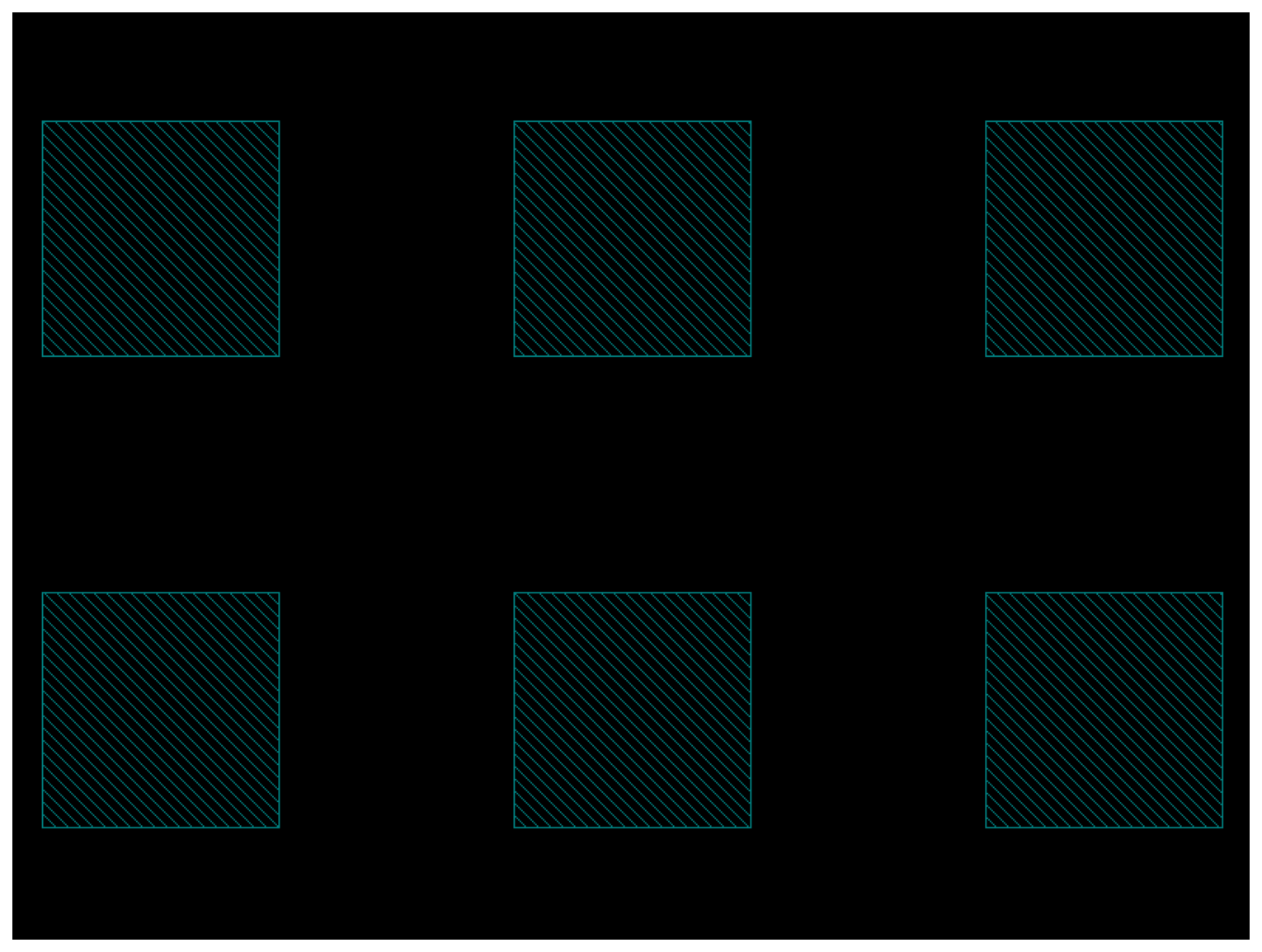
via_generator
via_generator(x_range=(0, 1), y_range=(0, 1), via_size=(0.17, 0.17), via_layer=(66, 44), via_enclosure=(0.06, 0.06), via_spacing=(0.17, 0.17))
Return only vias withen the range xrange and yrange while enclosing by via_enclosure and set number of rows and number of columns according to ranges and via size and spacing.
Parameters:
| Name | Type | Description | Default |
|---|---|---|---|
x_range
|
Float2
|
dx range. |
(0, 1)
|
y_range
|
Float2
|
dy range. |
(0, 1)
|
via_size
|
Float2
|
via size. |
(0.17, 0.17)
|
via_layer
|
LayerSpec
|
via layer. |
(66, 44)
|
via_enclosure
|
Float2
|
via enclosure. |
(0.06, 0.06)
|
via_spacing
|
Float2
|
via spacing. |
(0.17, 0.17)
|
via_stack(x_range=(0, 1), y_range=(0, 1), metal_level=1, con_size=(0.22, 0.22), con_enc=0.07, m_enc=0.06, con_spacing=(0.28, 0.28), via_size=(0.22, 0.22), via_spacing=(0.28, 0.28), via_enc=(0.06, 0.06), base_layer=layer['metal1'], **kwargs)
Returns a via stack withen the range xrange and yrange and expecting the base_layer to be drawen.
Parameters:
| Name | Type | Description | Default |
|---|---|---|---|
x_range
|
Float2
|
dx range. |
(0, 1)
|
y_range
|
Float2
|
dy range. |
(0, 1)
|
metal_level
|
int
|
metal level. |
1
|
con_size
|
Size
|
contact size. |
(0.22, 0.22)
|
con_enc
|
float
|
contact enclosure. |
0.07
|
m_enc
|
float
|
metal enclosure. |
0.06
|
con_spacing
|
Spacing
|
contact spacing. |
(0.28, 0.28)
|
via_size
|
Size
|
via size. |
(0.22, 0.22)
|
via_spacing
|
Spacing
|
via spacing. |
(0.28, 0.28)
|
via_enc
|
Float2
|
via enclosure. |
(0.06, 0.06)
|
return via stack till the metal level indicated where : metal_level 1 : till m1 metal_level 2 : till m2 metal_level 3 : till m3 metal_level 4 : till m4 metal_level 5 : till m5 withen the range xrange and yrange and expecting the base_layer to be drawen
import gf180mcu

gf180mcu.PDK.activate()
c = gf180mcu._cells["via_generator"](x_range=(0, 1), y_range=(0, 1), via_size=(0.17, 0.17), via_layer=(66, 44), via_enclosure=(0.06, 0.06), via_spacing=(0.17, 0.17))
c.draw_ports()
c.plot()
via_stack
Returns a via stack withen the range xrange and yrange and expecting the base_layer to be drawen.
Parameters:
| Name | Type | Description | Default |
|---|---|---|---|
x_range
|
Float2
|
dx range. |
(0, 1)
|
y_range
|
Float2
|
dy range. |
(0, 1)
|
metal_level
|
int
|
metal level. |
1
|
con_size
|
Size
|
contact size. |
(0.22, 0.22)
|
con_enc
|
float
|
contact enclosure. |
0.07
|
m_enc
|
float
|
metal enclosure. |
0.06
|
con_spacing
|
Spacing
|
contact spacing. |
(0.28, 0.28)
|
via_size
|
Size
|
via size. |
(0.22, 0.22)
|
via_spacing
|
Spacing
|
via spacing. |
(0.28, 0.28)
|
via_enc
|
Float2
|
via enclosure. |
(0.06, 0.06)
|
return via stack till the metal level indicated where : metal_level 1 : till m1 metal_level 2 : till m2 metal_level 3 : till m3 metal_level 4 : till m4 metal_level 5 : till m5 withen the range xrange and yrange and expecting the base_layer to be drawen

import gf180mcu

gf180mcu.PDK.activate()
c = gf180mcu._cells["via_stack"](x_range=(0, 1), y_range=(0, 1), metal_level=1, con_size=(0.22, 0.22), con_enc=0.07, m_enc=0.06, con_spacing=(0.28, 0.28), via_size=(0.22, 0.22), via_spacing=(0.28, 0.28), via_enc=(0.06, 0.06), base_layer='metal1')
c.draw_ports()
c.plot()
wire_corner
Returns 45 degrees electrical corner wire.
Parameters:
| Name | Type | Description | Default |
|---|---|---|---|
cross_section
|
CrossSectionSpec
|
spec. |
'metal2'
|
width
|
float | None
|
optional width. Defaults to cross_section width. |
None
|

import gf180mcu

gf180mcu.PDK.activate()
c = gf180mcu._cells["wire_corner"](cross_section='metal2')
c.draw_ports()
c.plot()
wire_corner45
Returns 90 degrees electrical corner wire.
Parameters:
| Name | Type | Description | Default |
|---|---|---|---|
cross_section
|
CrossSectionSpec
|
spec. |
'metal2'
|
radius
|
float
|
ignored. |
10
|
width
|
float | None
|
optional width. Defaults to cross_section width. |
None
|
layer
|
LayerSpec | None
|
ignored. |
None
|
with_corner90_ports
|
bool
|
if True, adds ports at 90 degrees. |
True
|
import gf180mcu

gf180mcu.PDK.activate()
c = gf180mcu._cells["wire_corner45"](cross_section='metal2', radius=10, with_corner90_ports=True)
c.draw_ports()
c.plot()
Fixed Cells (BJT, eFuse)
efuse
Electronic fuse.
npn_00p54x02p00
NPN BJT 0.54um x 2.00um emitter.
npn_00p54x04p00
NPN BJT 0.54um x 4.00um emitter.
npn_00p54x08p00
NPN BJT 0.54um x 8.00um emitter.
npn_00p54x16p00
NPN BJT 0.54um x 16.00um emitter.
npn_05p00x05p00
NPN BJT 5.00um x 5.00um emitter.
npn_10p00x10p00
NPN BJT 10.00um x 10.00um emitter.
pnp_05p00x00p42
PNP BJT 5.00um x 0.42um emitter.
pnp_05p00x05p00
PNP BJT 5.00um x 5.00um emitter.
pnp_10p00x00p42
PNP BJT 10.00um x 0.42um emitter.
pnp_10p00x10p00
PNP BJT 10.00um x 10.00um emitter.