Skip to content

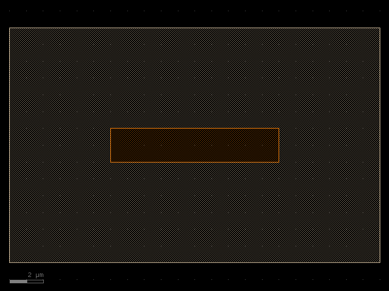
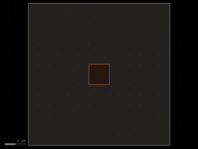
Parametric Cells

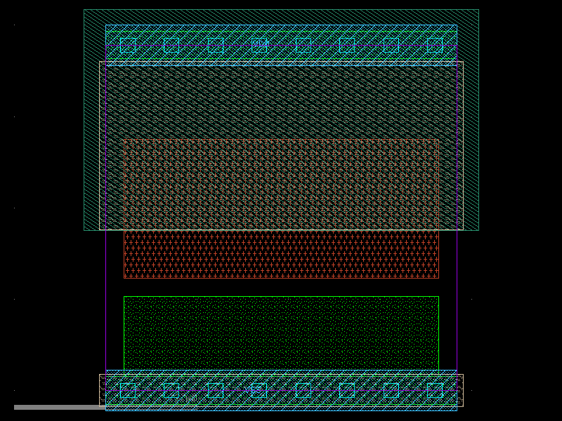
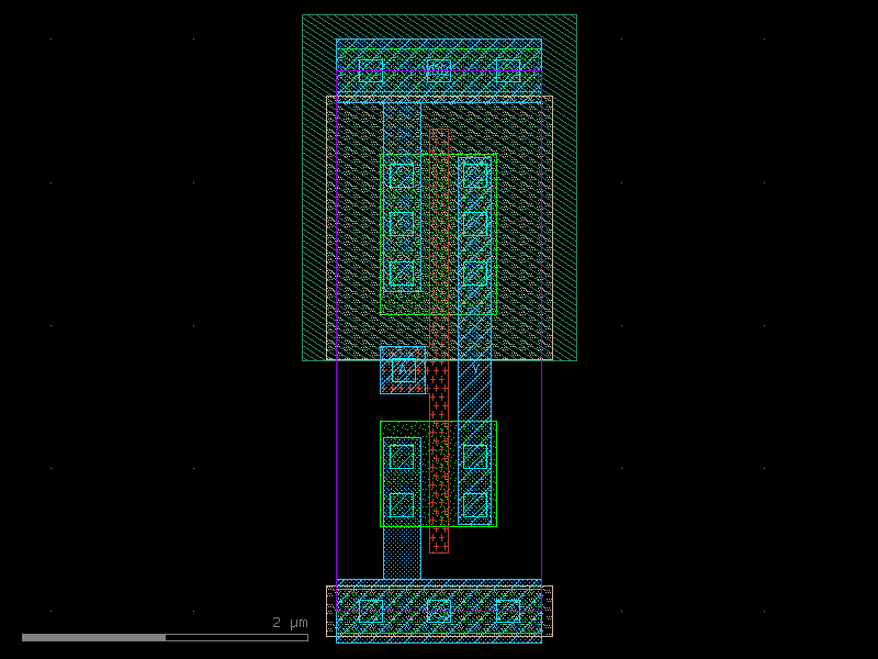
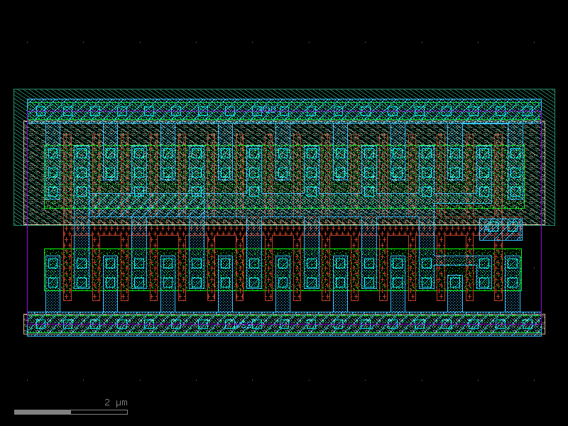
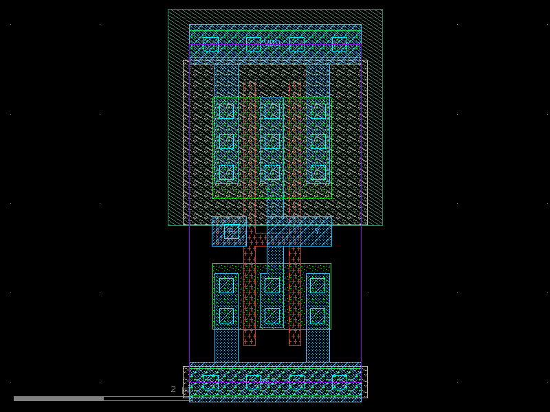
Here are the parametric components available in the PDK.

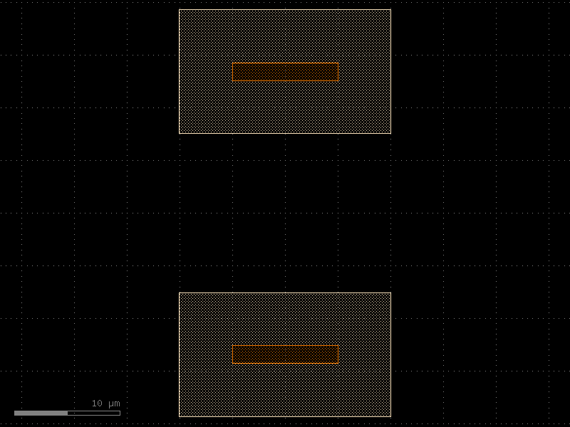
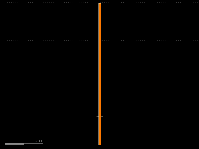
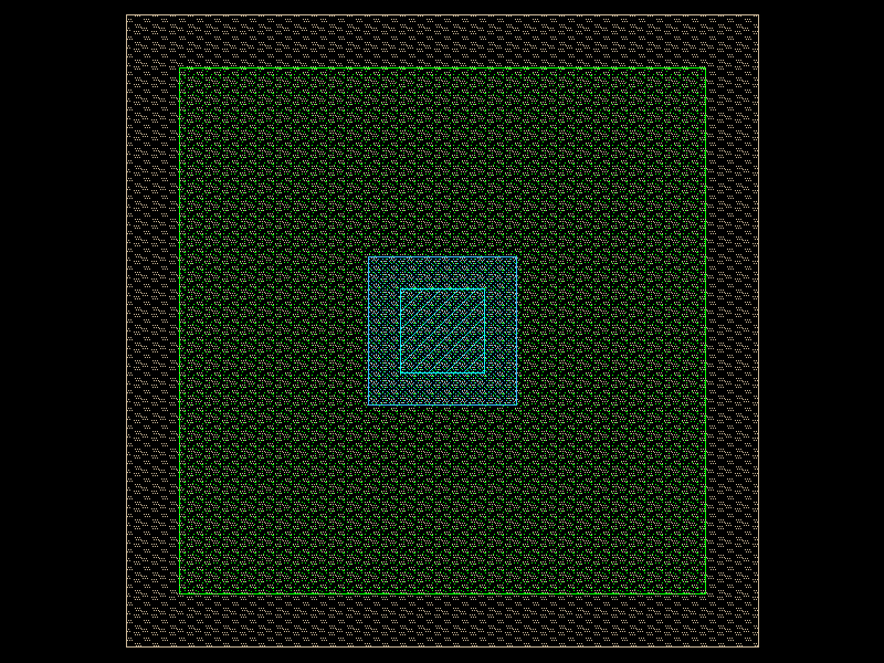
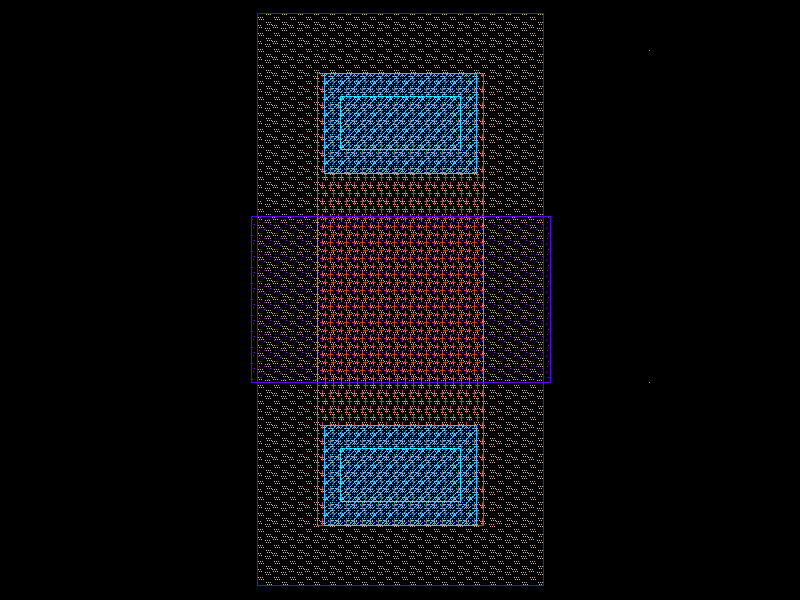
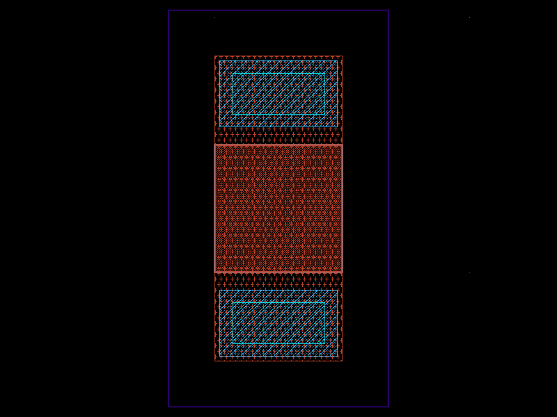
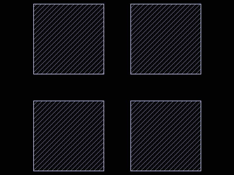
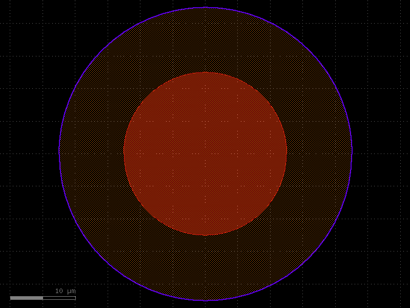
CuPillarPad

Returns CuPillarPad copper pillar pad (imported from GDS).

Source code in ihp/cells/bondpads.py
@gf.cell(tags=["IHP", "bondpad"])
def CuPillarPad() -> gf.Component:
    """Returns CuPillarPad copper pillar pad (imported from GDS)."""
    c = gf.import_gds(PATH.gds / "CuPillarPad.gds")
    width = 45
    c.add_port(
        name="e1", center=(0, 0), width=width, orientation=180, layer="TopMetal2drawing"
    )
    c.add_port(
        name="e2", center=(0, 0), width=width, orientation=0, layer="TopMetal2drawing"
    )
    c.add_port(
        name="e3", center=(0, 0), width=width, orientation=90, layer="TopMetal2drawing"
    )
    c.add_port(
        name="e4", center=(0, 0), width=width, orientation=270, layer="TopMetal2drawing"
    )
    return c

CuPillarPad

import warnings
warnings.filterwarnings("ignore", category=DeprecationWarning)

from ihp import PDK
from ihp import cells

PDK.activate()

c = cells.CuPillarPad().copy()
c.draw_ports()
c.plot()

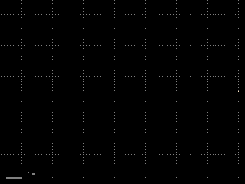
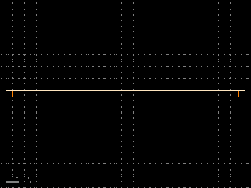
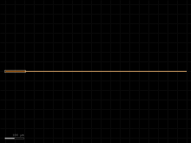
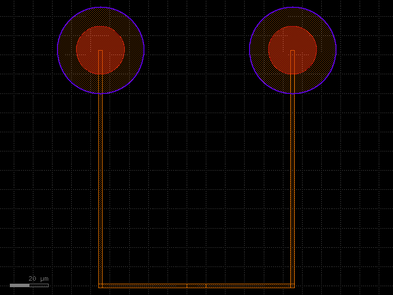
add_pads_top

Returns new component with ports connected top pads.

Parameters:

Name Type Description Default
component str | Callable[..., Component] | dict[str, Any] | DKCell | partial[Component]

component spec to connect to.

'straight'
port_names Sequence[str] | None

list of port names to connect to pads.

None
cross_section CrossSection | str | dict[str, Any] | Callable[..., CrossSection] | SymmetricalCrossSection | DCrossSection

cross_section function.

'metal_routing'
pad_port_name str

pad port name.

'e1'
pad str | Callable[..., Component] | dict[str, Any] | DKCell | partial[Component]

pad function.

CuPillarPad
bend str | Callable[..., Component] | dict[str, Any] | DKCell | partial[Component]

bend function.

'wire_corner'
straight_separation float

from edge to edge.

15.0
pad_pitch float

spacing between pads.

100.0
port_type str

port type.

'electrical'
allow_width_mismatch bool

if True, allows width mismatch.

True
fanout_length float | None

length of the fanout.

80
route_width float | list[float] | None

width of the route.

0
kwargs

additional arguments.

required
Example
import gdsfactory as gf
c = gf.c.nxn(
    xsize=600,
    ysize=200,
    north=2,
    south=3,
    wg_width=10,
    layer="M3",
    port_type="electrical",
)
cc = gf.routing.add_pads_top(component=c, port_names=("e1", "e4"), fanout_length=50)
cc.plot()
Source code in ihp/cells/containers.py
@gf.cell(tags=["IHP", "container"])
def add_pads_top(
    component: ComponentSpec = "straight",
    port_names: Strs | None = None,
    cross_section: CrossSectionSpec = "metal_routing",
    pad_port_name: str = "e1",
    pad: ComponentSpec = CuPillarPad,
    bend: ComponentSpec = "wire_corner",
    straight_separation: float = 15.0,
    pad_pitch: float = 100.0,
    port_type: str = "electrical",
    allow_width_mismatch: bool = True,
    fanout_length: float | None = 80,
    route_width: float | list[float] | None = 0,
    **kwargs,
) -> Component:
    """Returns new component with ports connected top pads.

    Args:
        component: component spec to connect to.
        port_names: list of port names to connect to pads.
        cross_section: cross_section function.
        pad_port_name: pad port name.
        pad: pad function.
        bend: bend function.
        straight_separation: from edge to edge.
        pad_pitch: spacing between pads.
        port_type: port type.
        allow_width_mismatch: if True, allows width mismatch.
        fanout_length: length of the fanout.
        route_width: width of the route.
        kwargs: additional arguments.

    Example:
        ```python
        import gdsfactory as gf
        c = gf.c.nxn(
            xsize=600,
            ysize=200,
            north=2,
            south=3,
            wg_width=10,
            layer="M3",
            port_type="electrical",
        )
        cc = gf.routing.add_pads_top(component=c, port_names=("e1", "e4"), fanout_length=50)
        cc.plot()
        ```

    """
    return gf.routing.add_pads_top(
        component=component,
        port_names=port_names,
        cross_section=cross_section,
        pad_port_name=pad_port_name,
        pad=pad,
        bend=bend,
        straight_separation=straight_separation,
        pad_pitch=pad_pitch,
        port_type=port_type,
        allow_width_mismatch=allow_width_mismatch,
        fanout_length=fanout_length,
        route_width=route_width,
        **kwargs,
    )

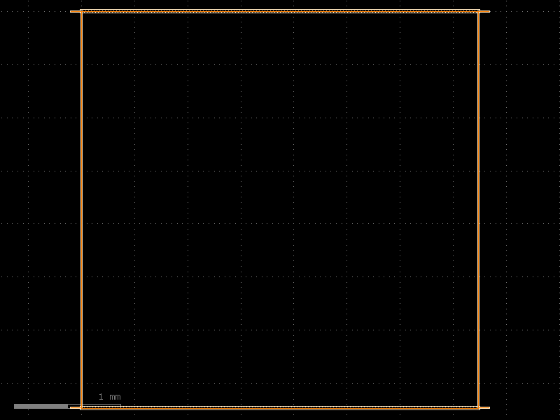
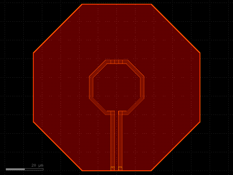
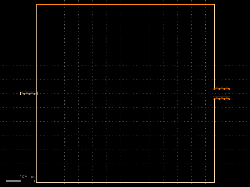
add_pads_top

import warnings
warnings.filterwarnings("ignore", category=DeprecationWarning)

from ihp import PDK
from ihp import cells

PDK.activate()

c = cells.add_pads_top(component='straight', cross_section='metal_routing', pad_port_name='e1', bend='wire_corner', straight_separation=15.0, pad_pitch=100.0, port_type='electrical', allow_width_mismatch=True, fanout_length=80, route_width=0).copy()
c.draw_ports()
c.plot()

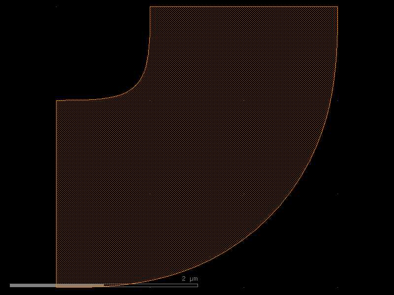
bend_euler

Regular degree euler bend.

Parameters:

Name Type Description Default
radius float | None

in um. Defaults to cross_section_radius.

None
angle float

total angle of the curve.

90
p float

Proportion of the curve that is an Euler curve.

0.5
width float | None

width to use. Defaults to cross_section.width.

None
cross_section CrossSection | str | dict[str, Any] | Callable[..., CrossSection] | SymmetricalCrossSection | DCrossSection

specification (CrossSection, string, CrossSectionFactory dict).

'strip'
allow_min_radius_violation bool

if True allows radius to be smaller than cross_section radius.

False
Source code in ihp/cells/waveguides.py
@gf.cell(tags=["IHP", "waveguide", "bend"])
def bend_euler(
    radius: float | None = None,
    angle: float = 90,
    p: float = 0.5,
    width: float | None = None,
    cross_section: CrossSectionSpec = "strip",
    allow_min_radius_violation: bool = False,
) -> gf.Component:
    """Regular degree euler bend.

    Args:
        radius: in um. Defaults to cross_section_radius.
        angle: total angle of the curve.
        p: Proportion of the curve that is an Euler curve.
        width: width to use. Defaults to cross_section.width.
        cross_section: specification (CrossSection, string, CrossSectionFactory dict).
        allow_min_radius_violation: if True allows radius to be smaller than cross_section radius.
    """
    return gf.c.bend_euler(
        radius=radius,
        angle=angle,
        p=p,
        width=width,
        cross_section=cross_section,
        allow_min_radius_violation=allow_min_radius_violation,
        with_arc_floorplan=True,
        npoints=None,
        layer=None,
    )

bend_euler

import warnings
warnings.filterwarnings("ignore", category=DeprecationWarning)

from ihp import PDK
from ihp import cells

PDK.activate()

c = cells.bend_euler(angle=90, p=0.5, cross_section='strip', allow_min_radius_violation=False).copy()
c.draw_ports()
c.plot()

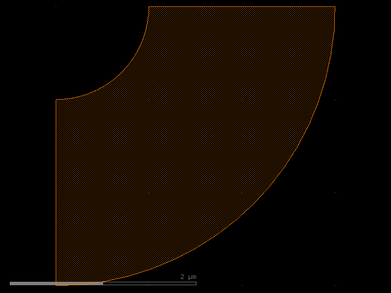
bend_metal

Regular degree euler bend.

Parameters:

Name Type Description Default
radius float | None

None.

None
angle float

90.

90
width float | None

None.

None
cross_section CrossSection | str | dict[str, Any] | Callable[..., CrossSection] | SymmetricalCrossSection | DCrossSection

"metal_routing".

'metal_routing'
Source code in ihp/cells/waveguides.py
@gf.cell(tags=["IHP", "wire", "bend"])
def bend_metal(
    radius: float | None = None,
    angle: float = 90,
    width: float | None = None,
    cross_section: CrossSectionSpec = "metal_routing",
) -> gf.Component:
    """Regular degree euler bend.

    Args:
        radius: None.
        angle: 90.
        width: None.
        cross_section: "metal_routing".
    """
    if radius is None:
        if width:
            xs = gf.get_cross_section(cross_section=cross_section, width=width)
        else:
            xs = gf.get_cross_section(cross_section=cross_section)
        radius = xs.radius or xs.width
    return gf.c.bend_circular(
        radius=radius,
        angle=angle,
        width=width,
        cross_section=cross_section,
        allow_min_radius_violation=True,
        npoints=None,
        layer=None,
    )

bend_metal

import warnings
warnings.filterwarnings("ignore", category=DeprecationWarning)

from ihp import PDK
from ihp import cells

PDK.activate()

c = cells.bend_metal(angle=90, cross_section='metal_routing').copy()
c.draw_ports()
c.plot()

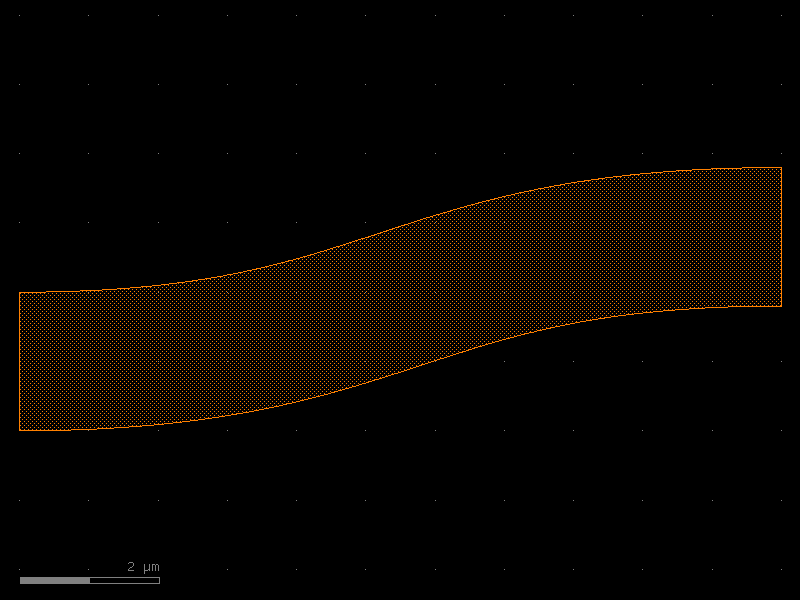
bend_s

Return S bend with bezier curve.

stores min_bend_radius property in self.info['min_bend_radius'] min_bend_radius depends on height and length

Parameters:

Name Type Description Default
size tuple[float, float]

in x and y direction.

(11, 1.8)
cross_section CrossSection | str | dict[str, Any] | Callable[..., CrossSection] | SymmetricalCrossSection | DCrossSection

spec.

'strip'
width float | None

width of the waveguide. If None, it will use the width of the cross_section.

None
allow_min_radius_violation bool

allows min radius violations.

False
Source code in ihp/cells/waveguides.py
@gf.cell(tags=["IHP", "waveguide", "bend"])
def bend_s(
    size: Size = (11, 1.8),
    cross_section: CrossSectionSpec = "strip",
    width: float | None = None,
    allow_min_radius_violation: bool = False,
) -> gf.Component:
    """Return S bend with bezier curve.

    stores min_bend_radius property in self.info['min_bend_radius']
    min_bend_radius depends on height and length

    Args:
        size: in x and y direction.
        cross_section: spec.
        width: width of the waveguide. If None, it will use the width of the cross_section.
        allow_min_radius_violation: allows min radius violations.
    """
    return gf.c.bend_s(
        size=size,
        cross_section=cross_section,
        npoints=99,
        allow_min_radius_violation=allow_min_radius_violation,
        width=width,
    )

bend_s

import warnings
warnings.filterwarnings("ignore", category=DeprecationWarning)

from ihp import PDK
from ihp import cells

PDK.activate()

c = cells.bend_s(size=(11, 1.8), cross_section='strip', allow_min_radius_violation=False).copy()
c.draw_ports()
c.plot()

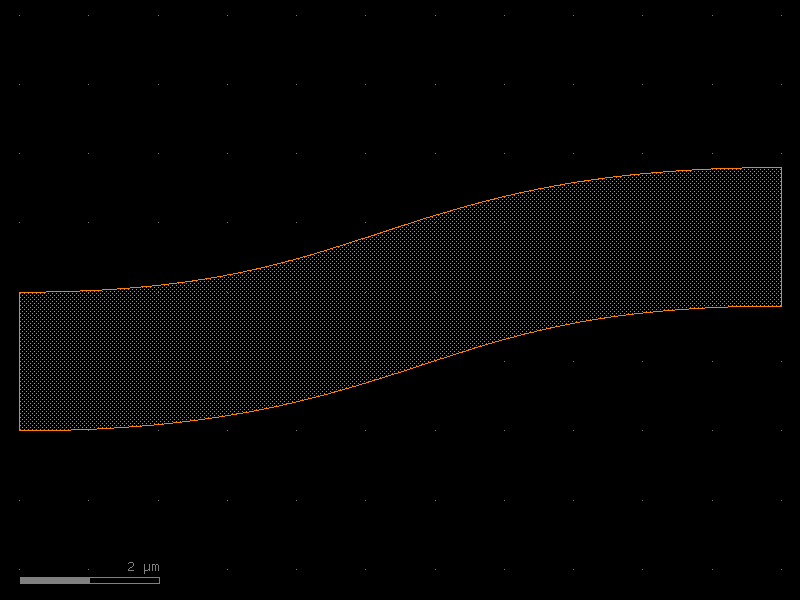
bend_s_metal

Return S bend with bezier curve.

stores min_bend_radius property in self.info['min_bend_radius'] min_bend_radius depends on height and length

Parameters:

Name Type Description Default
size tuple[float, float]

in x and y direction.

(11, 1.8)
cross_section CrossSection | str | dict[str, Any] | Callable[..., CrossSection] | SymmetricalCrossSection | DCrossSection

spec.

'metal_routing'
width float | None

width of the waveguide. If None, it will use the width of the cross_section.

None
allow_min_radius_violation bool

allows min radius violations.

True
Source code in ihp/cells/waveguides.py
@gf.cell(tags=["IHP", "wire", "bend"])
def bend_s_metal(
    size: Size = (11, 1.8),
    cross_section: CrossSectionSpec = "metal_routing",
    width: float | None = None,
    allow_min_radius_violation: bool = True,
) -> gf.Component:
    """Return S bend with bezier curve.

    stores min_bend_radius property in self.info['min_bend_radius']
    min_bend_radius depends on height and length

    Args:
        size: in x and y direction.
        cross_section: spec.
        width: width of the waveguide. If None, it will use the width of the cross_section.
        allow_min_radius_violation: allows min radius violations.
    """
    return gf.c.bend_s(
        size=size,
        cross_section=cross_section,
        npoints=99,
        allow_min_radius_violation=allow_min_radius_violation,
        width=width,
    )

bend_s_metal

import warnings
warnings.filterwarnings("ignore", category=DeprecationWarning)

from ihp import PDK
from ihp import cells

PDK.activate()

c = cells.bend_s_metal(size=(11, 1.8), cross_section='metal_routing', allow_min_radius_violation=True).copy()
c.draw_ports()
c.plot()

bondpad

Create a bondpad for wire bonding or flip-chip connection.

Parameters:

Name Type Description Default
shape Literal['octagon', 'square', 'circle']

Shape of the top-metal bondpad ("octagon", "square", or "circle").

'octagon'
diameter float

Interpreted as across-flats for octagons / squares, and diameter for circles.

80.0
layer_top_metal tuple[int, int] | str | int | LayerEnum

Top metal layer.

'TopMetal2drawing'
layer_passiv tuple[int, int] | str | int | LayerEnum

Passivation-opening layer.

'Passivpillar'
layer_dfpad tuple[int, int] | str | int | LayerEnum

Deep-fill or density-fill support layer.

'dfpaddrawing'
bbox_offsets tuple[float, ...] | None

Per-layer expansion distances in micrometers, applied to the passivation and dfpad layers.

(-2.1, 0)
flip_chip bool

If True, suppress passivation opening for flip-chip bumps.

False

Returns:

Type Description
Component

Component containing the complete bondpad stack.

Source code in ihp/cells/bondpads.py
@gf.cell(schematic_function=bondpad_schematic, tags=["IHP", "bondpad"])
def bondpad(
    shape: Literal["octagon", "square", "circle"] = "octagon",
    diameter: float = 80.0,
    layer_top_metal: LayerSpec = "TopMetal2drawing",
    layer_top_metal_pin: LayerSpec = "TopMetal2pin",
    layer_passiv: LayerSpec = "Passivpillar",
    layer_dfpad: LayerSpec = "dfpaddrawing",
    bbox_offsets: tuple[float, ...] | None = (-2.1, 0),
    flip_chip: bool = False,
) -> gf.Component:
    """Create a bondpad for wire bonding or flip-chip connection.

    Args:
        shape: Shape of the top-metal bondpad ("octagon", "square", or "circle").
        diameter: Interpreted as across-flats for octagons / squares, and diameter for circles.
        layer_top_metal: Top metal layer.
        layer_passiv: Passivation-opening layer.
        layer_dfpad: Deep-fill or density-fill support layer.
        bbox_offsets: Per-layer expansion distances in micrometers, applied to the passivation and dfpad layers.
        flip_chip: If True, suppress passivation opening for flip-chip bumps.

    Returns:
        Component containing the complete bondpad stack.
    """

    c = gf.Component()
    d = float(diameter)

    # Add top metal layer
    if shape == "square":
        c.add_ref(
            gf.components.rectangle(size=(d, d), layer=layer_top_metal, centered=True)
        )

    elif shape == "octagon":
        pts = regular_octagon_points(d)
        c.add_polygon(points=pts, layer=layer_top_metal)

    elif shape == "circle":
        c.add_ref(gf.components.circle(radius=d / 2, layer=layer_top_metal))

    else:
        raise ValueError(f"Unknown shape: {shape}")

    # Add additional layers
    if flip_chip:
        # Skip passivation opening for flip-chip
        bbox_layers = (layer_dfpad,)
        bbox_offsets = (bbox_offsets or ())[1:]
    else:
        bbox_layers = (layer_passiv, layer_dfpad)

    for layer, offset in zip(bbox_layers, bbox_offsets or ()):
        new_d = d + float(offset * 2)

        if shape == "square":
            c.add_ref(
                gf.components.rectangle(size=(new_d, new_d), layer=layer, centered=True)
            )
        elif shape == "circle":
            c.add_ref(gf.components.circle(radius=new_d / 2, layer=layer))
        elif shape == "octagon":
            c.add_polygon(points=regular_octagon_points(new_d), layer=layer)

    # Add port
    c.add_port(
        name="pad",
        center=(0, 0),
        width=d,
        orientation=0,
        layer=layer_top_metal_pin,
        port_type="electrical",
    )

    # Add metadata
    c.info["shape"] = shape
    c.info["diameter"] = diameter
    c.info["top_metal"] = layer_top_metal

    return c

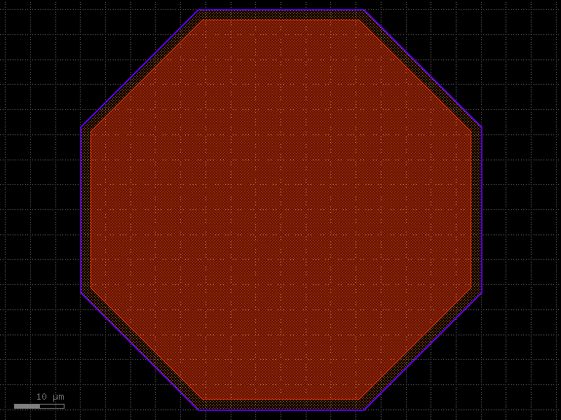
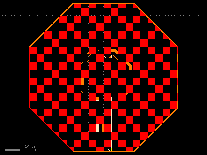
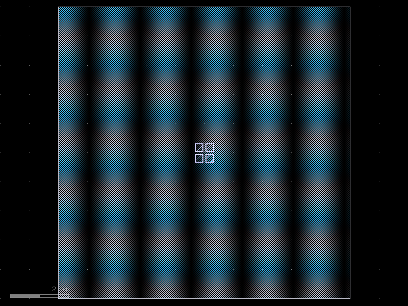
bondpad

import warnings
warnings.filterwarnings("ignore", category=DeprecationWarning)

from ihp import PDK
from ihp import cells

PDK.activate()

c = cells.bondpad(shape='octagon', diameter=80.0, layer_top_metal='TopMetal2drawing', layer_top_metal_pin='TopMetal2pin', layer_passiv='Passivpillar', layer_dfpad='dfpaddrawing', bbox_offsets=(-2.1, 0), flip_chip=False).copy()
c.draw_ports()
c.plot()

bondpad_array

Create an array of bondpads.

Parameters:

Name Type Description Default
n_pads int

Number of bondpads.

4
pad_pitch float

Pitch between bondpad centers in micrometers.

100.0
pad_diameter float

Diameter of each bondpad in micrometers.

80.0
shape Literal['octagon', 'square', 'circle']

Shape of the bondpads.

'octagon'
layer_top_metal tuple[int, int] | str | int | LayerEnum

Top metal layer for the bondpad.

'TopMetal2drawing'
layer_passiv tuple[int, int] | str | int | LayerEnum

Passivation layer.

'Passivpillar'
layer_dfpad tuple[int, int] | str | int | LayerEnum

Deep fill pad layer.

'dfpaddrawing'
bbox_offsets tuple[float, ...] | None

Offsets for each additional layer.

(-2.1, 0)

Returns:

Type Description
Component

Component with bondpad array.

Source code in ihp/cells/bondpads.py
@gf.cell(tags=["IHP", "bondpad", "array"])
def bondpad_array(
    n_pads: int = 4,
    pad_pitch: float = 100.0,
    pad_diameter: float = 80.0,
    shape: Literal["octagon", "square", "circle"] = "octagon",
    layer_top_metal: LayerSpec = "TopMetal2drawing",
    layer_top_metal_pin: LayerSpec = "TopMetal2pin",
    layer_passiv: LayerSpec = "Passivpillar",
    layer_dfpad: LayerSpec = "dfpaddrawing",
    bbox_offsets: tuple[float, ...] | None = (-2.1, 0),
) -> Component:
    """Create an array of bondpads.

    Args:
        n_pads: Number of bondpads.
        pad_pitch: Pitch between bondpad centers in micrometers.
        pad_diameter: Diameter of each bondpad in micrometers.
        shape: Shape of the bondpads.
        layer_top_metal: Top metal layer for the bondpad.
        layer_passiv: Passivation layer.
        layer_dfpad: Deep fill pad layer.
        bbox_offsets: Offsets for each additional layer.

    Returns:
        Component with bondpad array.
    """
    c = Component()

    for i in range(n_pads):
        pad = bondpad(
            shape=shape,
            diameter=pad_diameter,
            layer_top_metal=layer_top_metal,
            layer_top_metal_pin=layer_top_metal_pin,
            layer_passiv=layer_passiv,
            layer_dfpad=layer_dfpad,
            bbox_offsets=bbox_offsets,
        )
        pad_ref = c.add_ref(pad)
        pad_ref.movex(i * pad_pitch)

        # Add port for each pad
        c.add_port(
            name=f"pad_{i + 1}",
            center=(i * pad_pitch, 0),
            width=pad_diameter,
            orientation=0,
            layer=pad.ports["pad"].layer,
            port_type="electrical",
        )

    c.info["n_pads"] = n_pads
    c.info["pad_pitch"] = pad_pitch
    c.info["pad_diameter"] = pad_diameter

    # TODO: Bondpad array VLSIR Metadata

    return c

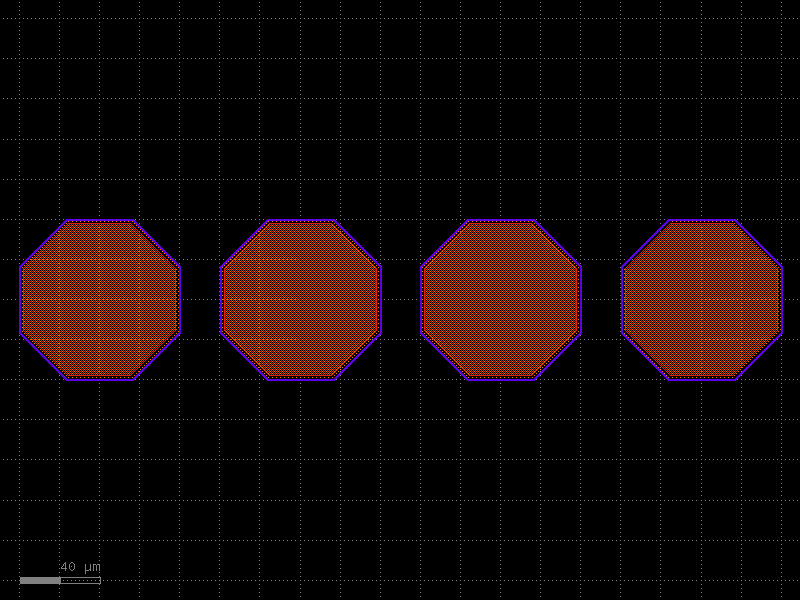
bondpad_array

import warnings
warnings.filterwarnings("ignore", category=DeprecationWarning)

from ihp import PDK
from ihp import cells

PDK.activate()

c = cells.bondpad_array(n_pads=4, pad_pitch=100.0, pad_diameter=80.0, shape='octagon', layer_top_metal='TopMetal2drawing', layer_top_metal_pin='TopMetal2pin', layer_passiv='Passivpillar', layer_dfpad='dfpaddrawing', bbox_offsets=(-2.1, 0)).copy()
c.draw_ports()
c.plot()

branch_line_coupler

Returns a branch line coupler coplanar transmission line.

Creates signal and ground lines for a branch line coupler.

Parameters:

Name Type Description Default
connection_length float

Length of the input line.

100
frequency float

Operating frequency (Hz).

10000000000.0
signal_cross_section CrossSection | str | dict[str, Any] | Callable[..., CrossSection] | SymmetricalCrossSection | DCrossSection

Cross-section for the signal line.

'topmetal2_routing'
ground_cross_section CrossSection | str | dict[str, Any] | Callable[..., CrossSection] | SymmetricalCrossSection | DCrossSection

Cross-section for the ground line.

'topmetal1_routing'
Z0 float

Target characteristic impedance (ohms).

50
e_r float

Relative permittivity of the substrate. Defaults to 4.1 for silicon dioxide.

4.1
Source code in ihp/cells/rf_devices.py
@gf.cell
def branch_line_coupler(
    connection_length: float = 100,
    frequency: float = 10e9,
    signal_cross_section: CrossSectionSpec = "topmetal2_routing",
    ground_cross_section: CrossSectionSpec = "topmetal1_routing",
    Z0: float = 50,
    e_r: float = 4.1,
) -> gf.Component:
    """Returns a branch line coupler coplanar transmission line.

    Creates signal and ground lines for a branch line coupler.

    Args:
        connection_length: Length of the input line.
        frequency: Operating frequency (Hz).
        signal_cross_section: Cross-section for the signal line.
        ground_cross_section: Cross-section for the ground line.
        Z0: Target characteristic impedance (ohms).
        e_r: Relative permittivity of the substrate. Defaults to 4.1 for silicon dioxide.
    """
    wave_length = 3e8 / frequency * 1e6

    c = gf.Component()

    corner = gf.Component()

    # calculate the needed widths
    width_Z0 = _calculate_width_from_Z0(
        Z0=Z0,
        ground_cross_section=ground_cross_section,
        signal_cross_section=signal_cross_section,
        e_r=e_r,
    )
    width_Z0_sqrt2 = _calculate_width_from_Z0(
        Z0=Z0 / sqrt(2),
        ground_cross_section=ground_cross_section,
        signal_cross_section=signal_cross_section,
        e_r=e_r,
    )
    e_eff = _calculate_effective_dielectric_constant(
        signal_cross_section=signal_cross_section,
        ground_cross_section=ground_cross_section,
        e_r=e_r,
    )

    quater_wave_length = wave_length / 4 / sqrt(e_eff)
    quater_wave_length = quater_wave_length - quater_wave_length % (
        tech.nm
    )  # truncate to 5 nm

    # create corner component for the 4 corners of the coupler
    corner.add_polygon(
        points=[
            (0, 0),
            (0, width_Z0),
            (width_Z0 - (width_Z0_sqrt2 - width_Z0), width_Z0),
            (width_Z0, width_Z0_sqrt2),
            (width_Z0, 0),
        ],
        layer=gf.get_cross_section(signal_cross_section).layer,
    )
    corner.add_port(
        name="e1",
        center=(width_Z0 / 2, 0),
        width=width_Z0,
        orientation=270,
        port_type="electrical",
        layer=gf.get_cross_section(signal_cross_section).layer,
    )
    corner.add_port(
        name="e2",
        center=(width_Z0, width_Z0_sqrt2 / 2),
        width=width_Z0_sqrt2,
        orientation=0,
        port_type="electrical",
        layer=gf.get_cross_section(signal_cross_section).layer,
    )
    corner.add_port(
        name="e3",
        center=(0, width_Z0 / 2),
        width=width_Z0,
        orientation=180,
        port_type="electrical",
        layer=gf.get_cross_section(signal_cross_section).layer,
    )

    # start with the top left corner
    corner_nw = c.add_ref(corner)

    # create and connect the top Z0/sqrt(2) transmission line
    tline_top = c.add_ref(
        tline(
            length=quater_wave_length - width_Z0,
            signal_cross_section=signal_cross_section,
            ground_cross_section=ground_cross_section,
            width=width_Z0_sqrt2,
        )
    )

    tline_top.connect("e1", corner_nw.ports["e2"])

    # create and connect the top right corner
    corner_ne = c.add_ref(corner).mirror(p1=(0, 0), p2=(0, 1))

    corner_ne.connect("e2", tline_top.ports["e2"])

    # create and connect the left Z0 transmission line
    tline_left = c.add_ref(
        tline(
            length=quater_wave_length - width_Z0_sqrt2,
            signal_cross_section=signal_cross_section,
            ground_cross_section=ground_cross_section,
            width=width_Z0,
        )
    )

    tline_left.connect("e1", corner_nw.ports["e1"])

    # create and connect the bottom left corner
    corner_sw = c.add_ref(corner).mirror(p1=(0, 0), p2=(1, 0))

    corner_sw.connect("e1", tline_left.ports["e2"])

    # create and connect the bottom Z0/sqrt(2) transmission line
    tline_bottom = c.add_ref(
        tline(
            length=quater_wave_length - width_Z0,
            signal_cross_section=signal_cross_section,
            ground_cross_section=ground_cross_section,
            width=width_Z0_sqrt2,
        )
    )

    tline_bottom.connect("e1", corner_sw.ports["e2"])

    # create and connect the bottom right corner
    corner_se = (
        c.add_ref(corner).mirror(p1=(0, 0), p2=(1, 0)).mirror(p1=(0, 0), p2=(0, 1))
    )

    corner_se.connect("e2", tline_bottom.ports["e2"])

    # create and connect the right Z0 transmission line
    tline_right = c.add_ref(
        tline(
            length=quater_wave_length - width_Z0_sqrt2,
            signal_cross_section=signal_cross_section,
            ground_cross_section=ground_cross_section,
            width=width_Z0,
        )
    )

    tline_right.connect("e1", corner_ne.ports["e1"])

    # create and connect input/output lines
    connection1 = c.add_ref(
        tline(
            length=connection_length,
            signal_cross_section=signal_cross_section,
            ground_cross_section=ground_cross_section,
            width=width_Z0,
        )
    )

    connection1.connect("e1", corner_nw.ports["e3"])

    connection2 = c.add_ref(
        tline(
            length=connection_length,
            signal_cross_section=signal_cross_section,
            ground_cross_section=ground_cross_section,
            width=width_Z0,
        )
    )

    connection2.connect("e1", corner_ne.ports["e3"])

    connection3 = c.add_ref(
        tline(
            length=connection_length,
            signal_cross_section=signal_cross_section,
            ground_cross_section=ground_cross_section,
            width=width_Z0,
        )
    )

    connection3.connect("e1", corner_se.ports["e3"])

    connection4 = c.add_ref(
        tline(
            length=connection_length,
            signal_cross_section=signal_cross_section,
            ground_cross_section=ground_cross_section,
            width=width_Z0,
        )
    )

    connection4.connect("e1", corner_sw.ports["e3"])

    # add ports to the component
    c.add_port(name="e1", port=connection1.ports["e2"])
    c.add_port(name="e2", port=connection2.ports["e2"])
    c.add_port(name="e3", port=connection3.ports["e2"])
    c.add_port(name="e4", port=connection4.ports["e2"])

    return c

branch_line_coupler

import warnings
warnings.filterwarnings("ignore", category=DeprecationWarning)

from ihp import PDK
from ihp import cells

PDK.activate()

c = cells.branch_line_coupler(connection_length=100, frequency=10000000000.0, signal_cross_section='topmetal2_routing', ground_cross_section='topmetal1_routing', Z0=50, e_r=4.1).copy()
c.draw_ports()
c.plot()

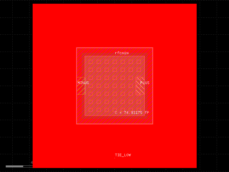
cmim

Create a MIM (Metal-Insulator-Metal) capacitor.

Parameters:

Name Type Description Default
width float

Width of the capacitor in micrometers.

6.0
length float

Length of the capacitor in micrometers.

6.0
bot_enclosure

Bottol Metal5 layer enclosure

required
top_enclosure
required
layer_metal5 tuple[int, int] | str | int | LayerEnum

Metal 5 drawing layer.

'Metal5drawing'
layer_mim tuple[int, int] | str | int | LayerEnum

MIM device drawing layer.

'MIMdrawing'
layer_vmim tuple[int, int] | str | int | LayerEnum

Vmim (MIM-TopMetal1 Via) drawing layer.

'Vmimdrawing'
layer_topmetal1 tuple[int, int] | str | int | LayerEnum

TopMetal1 drawing layer.

'TopMetal1drawing'
layer_cap_mark tuple[int, int] | str | int | LayerEnum

MemCap drawing layer.

'MemCapdrawing'
layer_m4nofill tuple[int, int] | str | int | LayerEnum

Metal4 nofill logic layer.

'Metal4nofill'
layer_m5nofill tuple[int, int] | str | int | LayerEnum

Metal5 nofill logic layer.

'Metal5nofill'
layer_tm1nofill tuple[int, int] | str | int | LayerEnum

TopMetal1 nofill logic layer.

'TopMetal1nofill'
layer_tm2nofill tuple[int, int] | str | int | LayerEnum

TopMetal2 nofill logic layer.

'TopMetal2nofill'
layer_text tuple[int, int] | str | int | LayerEnum

TEXT drawing layer.

'TEXTdrawing'
layer_metal5label tuple[int, int] | str | int | LayerEnum

Metal5 label logic layer.

'Metal5label'
layer_topmetal1label tuple[int, int] | str | int | LayerEnum

TopMetal1 label logic layer.

'TopMetal1label'
layer_metal5pin tuple[int, int] | str | int | LayerEnum

Metal5 pin logic layer.

'Metal5pin'
layer_topmetal1pin tuple[int, int] | str | int | LayerEnum

TopMetal1 pin logic layer.

'TopMetal1pin'
model str

Device model name.

'cmim'

Returns:

Type Description
Component

Component with MIM capacitor layout.

Raises:

Type Description
ValueError

If width or length is outside allowed range.

Source code in ihp/cells/capacitors.py
@gf.cell(schematic_function=cmim_schematic, tags=["IHP", "capacitor", "mim"])
def cmim(
    width: float = 6.0,
    length: float = 6.0,
    layer_metal5: LayerSpec = "Metal5drawing",
    layer_mim: LayerSpec = "MIMdrawing",
    layer_vmim: LayerSpec = "Vmimdrawing",
    layer_topmetal1: LayerSpec = "TopMetal1drawing",
    layer_cap_mark: LayerSpec = "MemCapdrawing",
    layer_m4nofill: LayerSpec = "Metal4nofill",
    layer_m5nofill: LayerSpec = "Metal5nofill",
    layer_tm1nofill: LayerSpec = "TopMetal1nofill",
    layer_tm2nofill: LayerSpec = "TopMetal2nofill",
    layer_text: LayerSpec = "TEXTdrawing",
    layer_metal5label: LayerSpec = "Metal5label",
    layer_topmetal1label: LayerSpec = "TopMetal1label",
    layer_metal5pin: LayerSpec = "Metal5pin",
    layer_topmetal1pin: LayerSpec = "TopMetal1pin",
    model: str = "cmim",
    **kwargs,
) -> Component:
    """Create a MIM (Metal-Insulator-Metal) capacitor.

    Args:
        width: Width of the capacitor in micrometers.
        length: Length of the capacitor in micrometers.
        bot_enclosure: Bottol Metal5 layer enclosure
        top_enclosure:
        layer_metal5: Metal 5 drawing layer.
        layer_mim: MIM device drawing layer.
        layer_vmim: Vmim (MIM-TopMetal1 Via) drawing layer.
        layer_topmetal1: TopMetal1 drawing layer.
        layer_cap_mark: MemCap drawing layer.
        layer_m4nofill: Metal4 nofill logic layer.
        layer_m5nofill: Metal5 nofill logic layer.
        layer_tm1nofill: TopMetal1 nofill logic layer.
        layer_tm2nofill: TopMetal2 nofill logic layer.
        layer_text: TEXT drawing layer.
        layer_metal5label: Metal5 label logic layer.
        layer_topmetal1label: TopMetal1 label logic layer.
        layer_metal5pin: Metal5 pin logic layer.
        layer_topmetal1pin: TopMetal1 pin logic layer.

        model: Device model name.

    Returns:
        Component with MIM capacitor layout.

    Raises:
        ValueError: If width or length is outside allowed range.
    """
    if width < tech.TECH.cmim_min_size or width > tech.TECH.cmim_max_size:
        raise ValueError(
            f"cmim width={width} out of range [{tech.TECH.cmim_min_size}, {tech.TECH.cmim_max_size}]"
        )
    if length < tech.TECH.cmim_min_size or length > tech.TECH.cmim_max_size:
        raise ValueError(
            f"cmim length={length} out of range [{tech.TECH.cmim_min_size}, {tech.TECH.cmim_max_size}]"
        )

    c = Component()

    mim_drc = {
        # capacitor
        "mim_min_size": tech.TECH.mim_min_size,
        "mim_cap_density": tech.TECH.mim_cap_density,
        # metals
        "m5_min_width": tech.TECH.metal5_width,
        "m5_min_spacing": tech.TECH.metal5_spacing,
        "topmetal1_width": tech.TECH.topmetal1_width,
        "topmetal1_spacing": tech.TECH.topmetal1_spacing,
        # vias
        "vmim_size": 0.42,
        "vmim_spacing": 0.52,
        "vmim_enc_metal": 0.42,
        "vmim_enc": 0.6,  # bot_enclosure
        "mim_enc": 0.36,  # top_enclosure
    }

    bot_enclosure = mim_drc["vmim_enc"]
    top_enclosure = mim_drc["mim_enc"]

    # snap to grid
    grid = tech.TECH.grid
    width = round(width / grid) * grid
    length = round(length / grid) * grid

    # build capacitor stack

    # Bottom plate (Metal4)
    bottom_plate_width = width + 2 * bot_enclosure + 2 * top_enclosure
    bottom_plate_length = length + 2 * bot_enclosure + 2 * top_enclosure

    bottom_plate = gf.components.rectangle(
        size=(bottom_plate_length, bottom_plate_width),
        layer=layer_metal5,
        centered=True,
    )
    bot = c.add_ref(bottom_plate)

    # MIM layer
    mim_layer = gf.components.rectangle(
        size=(length + 2 * top_enclosure, width + 2 * top_enclosure),
        layer=layer_mim,
        centered=True,
    )
    c.add_ref(mim_layer)

    # add vmim via array
    vmim_min_width = mim_drc["vmim_size"] + mim_drc["vmim_spacing"]
    nrows = int(floor(width / vmim_min_width))
    ncols = int(floor(length / vmim_min_width))

    # Top plate (TopMetal1)
    top_plate = gf.components.rectangle(
        size=(length, width),
        layer=layer_topmetal1,
        centered=True,
    )
    top = c.add_ref(top_plate)

    vmim_array = via_array(
        via_type=layer_vmim.split("drawing")[0],
        via_size=mim_drc["vmim_size"],
        via_spacing=mim_drc["vmim_size"] + mim_drc["vmim_spacing"],
        via_enclosure=mim_drc["vmim_enc_metal"],
        columns=ncols,
        rows=nrows,
    )
    vias = c.add_ref(vmim_array)
    vias.x = top.x
    vias.y = top.y

    # Add no fill logic layers

    logic = [
        layer_cap_mark,
        layer_m4nofill,
        layer_m5nofill,
        layer_tm1nofill,
        layer_tm2nofill,
    ]
    for layer_spec in logic:
        ll = gf.components.rectangle(
            size=(bottom_plate_length, bottom_plate_width),
            layer=layer_spec,
            centered=True,
        )
        c.add_ref(ll)

    minus = c.add_port(
        name="MINUS",
        center=(bot.xmin + mim_drc["m5_min_width"] / 2, bot.y),
        width=mim_drc["m5_min_width"],
        orientation=180,
        layer=layer_metal5pin,
        port_type="electrical",
    )

    plus = c.add_port(
        name="PLUS",
        center=(top.xmax - mim_drc["topmetal1_width"] / 2, top.y),
        width=mim_drc["topmetal1_width"],
        orientation=0,
        layer=layer_topmetal1pin,
        port_type="electrical",
    )

    pin_minus = gf.components.rectangle(
        size=(mim_drc["topmetal1_width"], 2 * mim_drc["topmetal1_width"]),
        layer=layer_metal5pin,
        centered=True,
    )
    pin_minus_ref = c.add_ref(pin_minus)
    pin_minus_ref.xmin = bot.xmin
    pin_minus_ref.y = minus.y

    pin_plus = gf.components.rectangle(
        size=(mim_drc["topmetal1_width"], 2 * mim_drc["topmetal1_width"]),
        layer=layer_topmetal1pin,
        centered=True,
    )
    pin_plus_ref = c.add_ref(pin_plus)
    pin_plus_ref.xmax = top.xmax
    pin_plus_ref.y = plus.y

    c.add_label(
        text="PLUS",
        position=(top.xmax - mim_drc["topmetal1_width"] / 2, top.y),
        layer=layer_text,
    )
    c.add_label(
        text="MINUS",
        position=(bot.xmin + mim_drc["m5_min_width"] / 2, bot.y),
        layer=layer_text,
    )

    c.add_label(text=model, position=(c.x, c.y + width / 2), layer=layer_text)

    # fringe_factor = kwargs.get("fringe_factor", 0.355)
    # capacitance = width * length * mim_drc['mim_cap_density']
    # capacitance *= (1+fringe_factor)
    capacitance = CbCapCalc("C", 0, length, width, model)

    c.add_label(
        text=f"C = {capacitance} fF", position=(c.x, c.y - width / 2), layer=layer_text
    )

    c.info["model"] = model
    c.info["width"] = width
    c.info["length"] = length
    c.info["capacitance_fF"] = capacitance
    c.info["area_um2"] = width * length

    return c

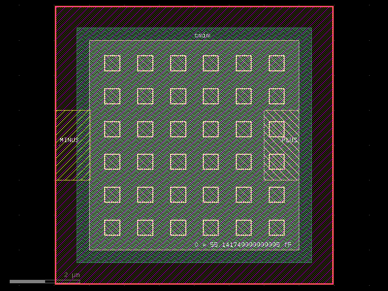
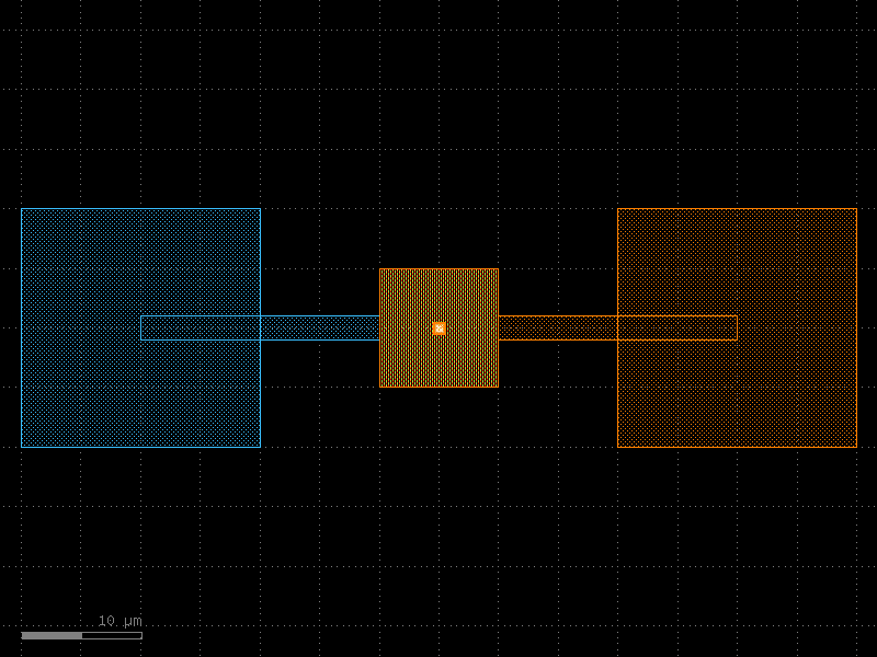
cmim

import warnings
warnings.filterwarnings("ignore", category=DeprecationWarning)

from ihp import PDK
from ihp import cells

PDK.activate()

c = cells.cmim(width=6.0, length=6.0, layer_metal5='Metal5drawing', layer_mim='MIMdrawing', layer_vmim='Vmimdrawing', layer_topmetal1='TopMetal1drawing', layer_cap_mark='MemCapdrawing', layer_m4nofill='Metal4nofill', layer_m5nofill='Metal5nofill', layer_tm1nofill='TopMetal1nofill', layer_tm2nofill='TopMetal2nofill', layer_text='TEXTdrawing', layer_metal5label='Metal5label', layer_topmetal1label='TopMetal1label', layer_metal5pin='Metal5pin', layer_topmetal1pin='TopMetal1pin', model='cmim').copy()
c.draw_ports()
c.plot()

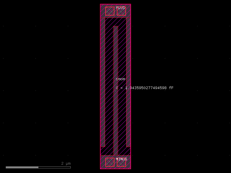
cmom

Create a MOM (Metal-Over-Metal) interdigitated capacitor.

Parameters:

Name Type Description Default
nfingers int

Number of inside fingers.

1
length float

Length of the capacitor in micrometers.

4.0
spacing float

Spacing between top and bottom electrodes. Higher spacing, lower capacitance.

0.26
botmetal tuple[int, int] | str | int | LayerEnum

Bottom Metal layer for the capacitor stack.

'Metal1'
topmetal tuple[int, int] | str | int | LayerEnum

Top Metal layer for the capacitor stack.

'Metal3'
layer_metal1 tuple[int, int] | str | int | LayerEnum

Metal1 drawing layer.

'Metal1drawing'
layer_metal2 tuple[int, int] | str | int | LayerEnum

Metal2 drawing layer.

'Metal2drawing'
layer_metal3 tuple[int, int] | str | int | LayerEnum

Metal3 drawing layer.

'Metal3drawing'
layer_metal4 tuple[int, int] | str | int | LayerEnum

Metal4 drawing layer.

'Metal4drawing'
layer_metal5 tuple[int, int] | str | int | LayerEnum

Metal5 drawing layer.

'Metal5drawing'
layer_metal1pin tuple[int, int] | str | int | LayerEnum

Metal1 pin logic layer.

'Metal1pin'
layer_metal2pin tuple[int, int] | str | int | LayerEnum

Metal2 pin logic layer.

'Metal2pin'
layer_metal3pin tuple[int, int] | str | int | LayerEnum

Metal3 pin logic layer.

'Metal3pin'
layer_metal4pin tuple[int, int] | str | int | LayerEnum

Metal4 pin logic layer.

'Metal4pin'
layer_metal5pin tuple[int, int] | str | int | LayerEnum

Metal5 pin logic layer.

'Metal5pin'
layer_metal1label tuple[int, int] | str | int | LayerEnum

Metal1 label logic layer.

'Metal1label'
layer_metal2label tuple[int, int] | str | int | LayerEnum

Metal2 label logic layer.

'Metal2label'
layer_metal3label tuple[int, int] | str | int | LayerEnum

Metal3 label logic layer.

'Metal3label'
layer_metal4label tuple[int, int] | str | int | LayerEnum

Metal4 label logic layer.

'Metal4label'
layer_metal5label tuple[int, int] | str | int | LayerEnum

Metal5 label logic layer.

'Metal5label'
layer_metal1nofill tuple[int, int] | str | int | LayerEnum

Metal1 nofill logic layer.

'Metal1nofill'
layer_metal2nofill tuple[int, int] | str | int | LayerEnum

Metal2 nofill logic layer.

'Metal2nofill'
layer_metal3nofill tuple[int, int] | str | int | LayerEnum

Metal3 nofill logic layer.

'Metal3nofill'
layer_metal4nofill tuple[int, int] | str | int | LayerEnum

Metal4 nofill logic layer.

'Metal4nofill'
layer_metal5nofill tuple[int, int] | str | int | LayerEnum

Metal5 nofill logic layer.

'Metal5nofill'
layer_cap_mark tuple[int, int] | str | int | LayerEnum

MemCapdrawing logic layer.

'MemCapdrawing'
layer_text tuple[int, int] | str | int | LayerEnum

TEXT drawing layer

'TEXTdrawing'
model str

Device model name.

'cmom'

Returns:

Type Description
Component

Component with MOM capacitor layout.

Raises:

Source code in ihp/cells/capacitors.py
@gf.cell(tags=["IHP", "capacitor", "mom"])
def cmom(
    nfingers: int = 1,
    length: float = 4.0,
    spacing: float = 0.26,
    botmetal: LayerSpec = "Metal1",
    topmetal: LayerSpec = "Metal3",
    layer_metal1: LayerSpec = "Metal1drawing",
    layer_metal2: LayerSpec = "Metal2drawing",
    layer_metal3: LayerSpec = "Metal3drawing",
    layer_metal4: LayerSpec = "Metal4drawing",
    layer_metal5: LayerSpec = "Metal5drawing",
    layer_metal1pin: LayerSpec = "Metal1pin",
    layer_metal2pin: LayerSpec = "Metal2pin",
    layer_metal3pin: LayerSpec = "Metal3pin",
    layer_metal4pin: LayerSpec = "Metal4pin",
    layer_metal5pin: LayerSpec = "Metal5pin",
    layer_metal1label: LayerSpec = "Metal1label",
    layer_metal2label: LayerSpec = "Metal2label",
    layer_metal3label: LayerSpec = "Metal3label",
    layer_metal4label: LayerSpec = "Metal4label",
    layer_metal5label: LayerSpec = "Metal5label",
    layer_metal1nofill: LayerSpec = "Metal1nofill",
    layer_metal2nofill: LayerSpec = "Metal2nofill",
    layer_metal3nofill: LayerSpec = "Metal3nofill",
    layer_metal4nofill: LayerSpec = "Metal4nofill",
    layer_metal5nofill: LayerSpec = "Metal5nofill",
    layer_cap_mark: LayerSpec = "MemCapdrawing",
    layer_text: LayerSpec = "TEXTdrawing",
    model: str = "cmom",
    **kwargs,
) -> Component:
    """Create a MOM (Metal-Over-Metal) interdigitated capacitor.

    Args:
        nfingers: Number of inside fingers.
        length: Length of the capacitor in micrometers.
        spacing: Spacing between top and bottom electrodes.
            Higher spacing, lower capacitance.
        botmetal: Bottom Metal layer for the capacitor stack.
        topmetal: Top Metal layer for the capacitor stack.
        --- Layers
        layer_metal1: Metal1 drawing layer.
        layer_metal2: Metal2 drawing layer.
        layer_metal3: Metal3 drawing layer.
        layer_metal4: Metal4 drawing layer.
        layer_metal5: Metal5 drawing layer.
        layer_metal1pin: Metal1 pin logic layer.
        layer_metal2pin: Metal2 pin logic layer.
        layer_metal3pin: Metal3 pin logic layer.
        layer_metal4pin: Metal4 pin logic layer.
        layer_metal5pin: Metal5 pin logic layer.
        layer_metal1label: Metal1 label logic layer.
        layer_metal2label: Metal2 label logic layer.
        layer_metal3label: Metal3 label logic layer.
        layer_metal4label: Metal4 label logic layer.
        layer_metal5label: Metal5 label logic layer.
        layer_metal1nofill: Metal1 nofill logic layer.
        layer_metal2nofill: Metal2 nofill logic layer.
        layer_metal3nofill: Metal3 nofill logic layer.
        layer_metal4nofill: Metal4 nofill logic layer.
        layer_metal5nofill: Metal5 nofill logic layer.
        layer_cap_mark: MemCapdrawing logic layer.
        layer_text: TEXT drawing layer
        model: Device model name.

    Returns:
        Component with MOM capacitor layout.
    Raises:
    """

    metals = {
        "Metal1": layer_metal1,
        "Metal2": layer_metal2,
        "Metal3": layer_metal3,
        "Metal4": layer_metal4,
        "Metal5": layer_metal5,
    }

    labels = {
        "Metal1": layer_metal1label,
        "Metal2": layer_metal2label,
        "Metal3": layer_metal3label,
        "Metal4": layer_metal4label,
        "Metal5": layer_metal5label,
    }

    pins = {
        "Metal1": layer_metal1pin,
        "Metal2": layer_metal2pin,
        "Metal3": layer_metal3pin,
        "Metal4": layer_metal4pin,
        "Metal5": layer_metal5pin,
    }

    nofills = {
        "Metal1": layer_metal1nofill,
        "Metal2": layer_metal2nofill,
        "Metal3": layer_metal3nofill,
        "Metal4": layer_metal4nofill,
        "Metal5": layer_metal5nofill,
    }

    pdk_design_rules = {
        "Metal1": {
            "min_width": tech.TECH.metal1_width,
            "min_spacing": tech.TECH.metal1_spacing,
        },
        "Metal2": {
            "min_width": tech.TECH.metal2_width,
            "min_spacing": tech.TECH.metal2_spacing,
        },
        "Metal3": {
            "min_width": tech.TECH.metal3_width,
            "min_spacing": tech.TECH.metal3_spacing,
        },
        "Metal4": {
            "min_width": tech.TECH.metal4_width,
            "min_spacing": tech.TECH.metal4_spacing,
        },
        "Metal5": {
            "min_width": tech.TECH.metal5_width,
            "min_spacing": tech.TECH.metal5_spacing,
        },
    }

    min_width_global = min([v["min_width"] for v in pdk_design_rules.values()])
    min_spacing_global = min([v["min_spacing"] for v in pdk_design_rules.values()])
    min_length = 3 * min_width_global  # to comply with minimum metal area DRC

    assert length > min_length, (
        f"Minimum Area for all metals > {min_length * min_width_global}"
    )
    assert spacing > min_spacing_global, (
        f"Minimum metal spacing for all metals > {min_spacing_global}"
    )

    ordered_metals = list(metals.keys())
    # ordered_vias = [lay for lay in ordered_layers if "via" in lay]
    assert botmetal in ordered_metals, (
        "{botmetal} not it available layers: {_ordered_metals}"
    )
    assert topmetal in ordered_metals, (
        "{topmetal} not it available layers: {_ordered_metals}"
    )
    mom_metals = ordered_metals[
        ordered_metals.index(botmetal) : ordered_metals.index(topmetal) + 1
    ]
    c = gf.Component()
    total_length = 0.0
    top_pad_ref = None
    bot_pad_ref = None
    for metal_layer in mom_metals:
        min_width = min_width_global
        layer = metals[metal_layer]
        top_finger = gf.components.rectangle(size=(min_width, length), layer=layer)
        top_finger_array = c.add_ref(
            top_finger,
            columns=nfingers + 1,
            rows=1,
            column_pitch=2 * (spacing + min_width),
        )
        top_finger_array.ymin += spacing
        bot_finger = gf.components.rectangle(size=(min_width, length), layer=layer)
        bot_finger_array = c.add_ref(
            bot_finger, columns=nfingers, rows=1, column_pitch=2 * (spacing + min_width)
        )
        bot_finger_array.xmin += min_width + spacing
        total_length = (min_width + spacing) * (2 * nfingers + 1) - spacing
        top_pad = gf.components.rectangle(
            size=(total_length, 3 * min_width), layer=layer
        )
        top_pad_ref = c.add_ref(top_pad)
        top_pad_ref.ymin += length + spacing
        bot_pad_ref = c.add_ref(top_pad)
        bot_pad_ref.ymax = 0

        #   add no fill and no QRC layers to the mom device region
        # nofill_layer = metal_layer.capitalize()+'nofill'
        nofill_layer = nofills[metal_layer.capitalize()]
        c.add_ref(gf.components.bbox(c, layer=nofill_layer))

    # add capacitor region marker
    c.add_ref(gf.components.bbox(c, layer=layer_cap_mark))

    # add ports
    # pin_layer: LayerSpec = metal_layer.capitalize()+'pin'
    # label_layer: LayerSpec = metal_layer.capitalize()+'label'
    pin_layer = pins[metal_layer.capitalize()]
    label_layer = labels[metal_layer.capitalize()]
    c.add_port(
        "PLUS",
        center=(top_pad_ref.x, top_pad_ref.y),
        width=min_width,
        layer=pin_layer,
        port_type="electrical",
    )
    c.add_port(
        "MINUS",
        center=(bot_pad_ref.x, bot_pad_ref.y),
        width=min_width,
        layer=pin_layer,
        port_type="electrical",
    )

    c.add_label(text="PLUS", position=(top_pad_ref.x, top_pad_ref.y), layer=label_layer)
    c.add_label(
        text="MINUS", position=(bot_pad_ref.x, bot_pad_ref.y), layer=label_layer
    )
    c.add_label(text="PLUS", position=(top_pad_ref.x, top_pad_ref.y), layer=layer_text)
    c.add_label(text="MINUS", position=(bot_pad_ref.x, bot_pad_ref.y), layer=layer_text)

    c.add_label(text=model, position=(c.x, c.y + min_width), layer=layer_text)

    #   add a via array stack to the top and bottom pads
    mom_via_stack = via_stack(
        bottom_layer=botmetal.capitalize(),
        top_layer=topmetal.capitalize(),
        size=(total_length, 3 * min_width),
        vn_columns=nfingers * 4,
        vn_rows=1,
    )

    via_stack_bot = c.add_ref(mom_via_stack)
    via_stack_bot.xmin = bot_pad_ref.xmin
    via_stack_bot.ymax = bot_pad_ref.ymax
    via_stack_top = c.add_ref(mom_via_stack)
    via_stack_top.xmin = top_pad_ref.xmin
    via_stack_top.ymin = top_pad_ref.ymin

    #   add place and route layers to define the device's bounding box
    prboundary_layer = "prBoundarydrawing"
    c.add_ref(gf.components.bbox(c, layer=prboundary_layer))
    c.info["capacitance"] = cmom_extractor(
        nfingers,
        length,
        spacing,
        min_width=min_width_global,
        mom_metals=mom_metals,
        **kwargs,
    )
    c.add_label(
        text=f"C = {c.info['capacitance']} fF",
        position=(c.x, c.y - min_width),
        layer=layer_text,
    )
    c.info["model"] = model
    c.info["nfingers"] = nfingers
    c.info["length"] = length
    c.info["spacing"] = spacing

    #   return the component
    return c

cmom

import warnings
warnings.filterwarnings("ignore", category=DeprecationWarning)

from ihp import PDK
from ihp import cells

PDK.activate()

c = cells.cmom(nfingers=1, length=4.0, spacing=0.26, botmetal='Metal1', topmetal='Metal3', layer_metal1='Metal1drawing', layer_metal2='Metal2drawing', layer_metal3='Metal3drawing', layer_metal4='Metal4drawing', layer_metal5='Metal5drawing', layer_metal1pin='Metal1pin', layer_metal2pin='Metal2pin', layer_metal3pin='Metal3pin', layer_metal4pin='Metal4pin', layer_metal5pin='Metal5pin', layer_metal1label='Metal1label', layer_metal2label='Metal2label', layer_metal3label='Metal3label', layer_metal4label='Metal4label', layer_metal5label='Metal5label', layer_metal1nofill='Metal1nofill', layer_metal2nofill='Metal2nofill', layer_metal3nofill='Metal3nofill', layer_metal4nofill='Metal4nofill', layer_metal5nofill='Metal5nofill', layer_cap_mark='MemCapdrawing', layer_text='TEXTdrawing', model='cmom').copy()
c.draw_ports()
c.plot()

coupled_line_bandpass_filter

Return a coupled-line bandpass filter.

Synthesises an N-th order coupled-line bandpass filter from Butterworth or Chebyshev lowpass prototype coefficients. Each section is realised as a pair of coupled coplanar transmission lines whose even/odd-mode impedances are derived from the prototype element values and the fractional bandwidth.

Parameters:

Name Type Description Default
order int

Filter order (number of resonators).

3
frequency float

Centre frequency (Hz).

10000000000.0
bandwidth float

Absolute bandwidth (Hz).

1000000000.0
connection_length float

Length of the input/output feed lines (um).

50
Z0 float

Reference characteristic impedance (ohms).

50
signal_cross_section CrossSection | str | dict[str, Any] | Callable[..., CrossSection] | SymmetricalCrossSection | DCrossSection

Cross-section for the signal line.

'topmetal2_routing'
ground_cross_section CrossSection | str | dict[str, Any] | Callable[..., CrossSection] | SymmetricalCrossSection | DCrossSection

Cross-section for the ground line.

'topmetal1_routing'
e_r float

Relative permittivity of the substrate. Defaults to 4.1 for silicon dioxide.

4.1
filter_type str

Prototype type — "butter" for Butterworth or "cheby" for Chebyshev.

'butter'
ripple_dB float

Pass-band ripple in dB (only used when filter_type is "cheby").

3

Returns:

Type Description
Component

A Component with ports e1 (input) and e2 (output).

Source code in ihp/cells/rf_devices.py
@gf.cell
def coupled_line_bandpass_filter(
    order: int = 3,
    frequency: float = 10e9,
    bandwidth: float = 1e9,
    connection_length: float = 50,
    Z0: float = 50,
    signal_cross_section: CrossSectionSpec = "topmetal2_routing",
    ground_cross_section: CrossSectionSpec = "topmetal1_routing",
    e_r: float = 4.1,
    filter_type: str = "butter",
    ripple_dB: float = 3,
) -> gf.Component:
    """Return a coupled-line bandpass filter.

    Synthesises an *N*-th order coupled-line bandpass filter from
    Butterworth or Chebyshev lowpass prototype coefficients.  Each
    section is realised as a pair of coupled coplanar transmission
    lines whose even/odd-mode impedances are derived from the
    prototype element values and the fractional bandwidth.

    Args:
        order: Filter order (number of resonators).
        frequency: Centre frequency (Hz).
        bandwidth: Absolute bandwidth (Hz).
        connection_length: Length of the input/output feed lines (um).
        Z0: Reference characteristic impedance (ohms).
        signal_cross_section: Cross-section for the signal line.
        ground_cross_section: Cross-section for the ground line.
        e_r: Relative permittivity of the substrate.
            Defaults to 4.1 for silicon dioxide.
        filter_type: Prototype type — ``"butter"`` for Butterworth or
            ``"cheby"`` for Chebyshev.
        ripple_dB: Pass-band ripple in dB (only used when
            *filter_type* is ``"cheby"``).

    Returns:
        A Component with ports ``e1`` (input) and ``e2`` (output).
    """

    c = gf.Component()
    # get filter coefficients
    # g = [g1 g2 ... gN gN+1] for N-th order filter
    if filter_type == "butter":
        g = _butterworth_prototype(order)
    elif filter_type == "cheby":
        g = _chebyshev_prototype(order, ripple_dB)

    fractional_bandwidth = bandwidth / frequency
    f_2 = frequency * (1 + fractional_bandwidth / 2)
    f_1 = frequency * (1 - fractional_bandwidth / 2)

    delta = fractional_bandwidth

    # initialize lists for Z0J values
    Z0J = [0.0] * (order + 1)

    # first Z0J value
    Z0J[0] = sqrt(pi * delta / (2 * g[0]))

    # calculate Z0J values for j = 1 to N-1
    for j in range(1, order):
        Z0J[j] = pi * delta / (2 * sqrt(g[j - 1] * g[j]))

    # last Z0J value
    Z0J[order] = sqrt(pi * delta / (2 * g[order - 1] * g[order]))

    # initialize and calculate Z0e and Z0o values for each section
    Z0e = [0.0] * (order + 1)
    Z0o = [0.0] * (order + 1)
    Z_section = [0.0] * (order + 1)

    for j in range(order + 1):
        Z0e[j] = Z0 * (1 + Z0J[j] + Z0J[j] ** 2)
        Z0o[j] = Z0 * (1 - Z0J[j] + Z0J[j] ** 2)

        Z_section[j] = sqrt(Z0e[j] * Z0o[j])

    # calculate the coupling coefficient k for each section
    g = [1.0] + g  # prepend g0 = 1.0 for easier indexing
    k = [0.0] * (order + 1)
    for j in range(order + 1):
        k[j] = (f_2 - f_1) / sqrt(f_1 * f_2 * g[j] * g[j + 1])

    e_eff = _calculate_effective_dielectric_constant(
        signal_cross_section=signal_cross_section,
        ground_cross_section=ground_cross_section,
        e_r=e_r,
    )
    segment_length = scipy.constants.c / frequency * 1e6 / sqrt(e_eff) / 4
    segment_length = segment_length - segment_length % tech.nm  # snap to grid

    connection_in = c.add_ref(
        tline(
            length=connection_length,
            signal_cross_section=signal_cross_section,
            ground_cross_section=ground_cross_section,
            Z0=Z0,
        )
    )

    connection_out = c.add_ref(
        tline(
            length=connection_length,
            signal_cross_section=signal_cross_section,
            ground_cross_section=ground_cross_section,
            Z0=Z0,
        )
    )

    previous_section = connection_in

    for i in range(order + 1):
        section_i = c.add_ref(
            coupler_tline(
                Z0e=Z0e[i],
                Z0o=Z0o[i],
                length=segment_length,
                signal_cross_section=signal_cross_section,
                ground_cross_section=ground_cross_section,
            )
        )
        section_i.connect("e4", previous_section.ports["e2"], allow_width_mismatch=True)
        previous_section = section_i

    connection_out.connect(
        "e1", previous_section.ports["e2"], allow_width_mismatch=True
    )

    c.add_port(name="e1", port=connection_in.ports["e1"])
    c.add_port(name="e2", port=connection_out.ports["e2"])

    c.flatten()

    return c

coupled_line_bandpass_filter

import warnings
warnings.filterwarnings("ignore", category=DeprecationWarning)

from ihp import PDK
from ihp import cells

PDK.activate()

c = cells.coupled_line_bandpass_filter(order=3, frequency=10000000000.0, bandwidth=1000000000.0, connection_length=50, Z0=50, signal_cross_section='topmetal2_routing', ground_cross_section='topmetal1_routing', e_r=4.1, filter_type='butter', ripple_dB=3).copy()
c.draw_ports()
c.plot()

coupler_tline

Return a straight coupled coplanar transmission line.

Creates two parallel signal lines separated by a gap, with a shared ground plane underneath (and optionally above for stripline). The ground plane extends 3x the signal width beyond each end of the signal lines and is wide enough to cover both lines plus margins.

Parameters:

Name Type Description Default
length float

Length of the signal lines (um).

10
gap

Spacing between the two signal lines (um).

required
signal_cross_section CrossSection | str | dict[str, Any] | Callable[..., CrossSection] | SymmetricalCrossSection | DCrossSection

Cross-section for the signal lines.

'topmetal2_routing'
ground_cross_section CrossSection | str | dict[str, Any] | Callable[..., CrossSection] | SymmetricalCrossSection | DCrossSection

Cross-section for the ground plane. Accepts a single spec for microstrip or a two-element list [lower, upper] for stripline.

'topmetal1_routing'
width

Signal line width (um). Mutually exclusive with Z0.

required
Z0

Target characteristic impedance (ohms). Mutually exclusive with width.

required
npoints int

Number of points used to draw the straights.

2

Returns:

Type Description
Component

A Component containing two coupled signal lines (with ports

Component

prefixed top_ and bot_) and ground plane(s).

Raises:

Type Description
ValueError

If neither or both of width and Z0 are provided.

Source code in ihp/cells/waveguides.py
@gf.cell
def coupler_tline(
    Z0e: float = 50,
    Z0o: float = 50,
    length: float = 10,
    signal_cross_section: CrossSectionSpec = "topmetal2_routing",
    ground_cross_section: CrossSectionSpec = "topmetal1_routing",
    e_r: float = 4.1,
    npoints: int = 2,
) -> gf.Component:
    """Return a straight coupled coplanar transmission line.

    Creates two parallel signal lines separated by a gap, with a shared
    ground plane underneath (and optionally above for stripline).  The
    ground plane extends 3x the signal width beyond each end of the
    signal lines and is wide enough to cover both lines plus margins.

    Args:
        length: Length of the signal lines (um).
        gap: Spacing between the two signal lines (um).
        signal_cross_section: Cross-section for the signal lines.
        ground_cross_section: Cross-section for the ground plane.
            Accepts a single spec for microstrip or a two-element list
            ``[lower, upper]`` for stripline.
        width: Signal line width (um). Mutually exclusive with Z0.
        Z0: Target characteristic impedance (ohms). Mutually exclusive
            with width.
        npoints: Number of points used to draw the straights.

    Returns:
        A Component containing two coupled signal lines (with ports
        prefixed ``top_`` and ``bot_``) and ground plane(s).

    Raises:
        ValueError: If neither or both of *width* and *Z0* are provided.
    """
    Z0 = sqrt(Z0e * Z0o)

    width = _calculate_width_from_Z0(
        Z0=Z0,
        ground_cross_section=ground_cross_section,
        signal_cross_section=signal_cross_section,
        e_r=e_r,
    )

    h, t = _get_stack_geometry(signal_cross_section, ground_cross_section)

    # calculate separation gap from even and odd mode impedances
    # https://www.dmcrf.com/microstrip-calculators/differential-microstrip-impedance-calculator/
    Z_d = 2 * Z0o
    d = (
        -h
        / 0.98
        * log(1 - (Z_d * sqrt(e_r + 1.41)) / (174 * log(5.98 * h / (0.8 * width + t))))
    )

    c = gf.Component()

    top = c.add_ref(
        tline(
            length=length,
            signal_cross_section=signal_cross_section,
            ground_cross_section=ground_cross_section,
            width=width,
            npoints=npoints,
        )
    )
    top.movey(d / 2 + width / 2)

    bot = c.add_ref(
        tline(
            length=length,
            signal_cross_section=signal_cross_section,
            ground_cross_section=ground_cross_section,
            width=width,
            npoints=npoints,
        )
    )
    bot.movey(-d / 2 - width / 2)

    c.add_port(name="e1", port=top.ports["e1"])
    c.add_port(name="e2", port=top.ports["e2"])
    c.add_port(name="e3", port=bot.ports["e2"])
    c.add_port(name="e4", port=bot.ports["e1"])
    c.flatten()

    return c

coupler_tline

import warnings
warnings.filterwarnings("ignore", category=DeprecationWarning)

from ihp import PDK
from ihp import cells

PDK.activate()

c = cells.coupler_tline(Z0e=50, Z0o=50, length=10, signal_cross_section='topmetal2_routing', ground_cross_section='topmetal1_routing', e_r=4.1, npoints=2).copy()
c.draw_ports()
c.plot()

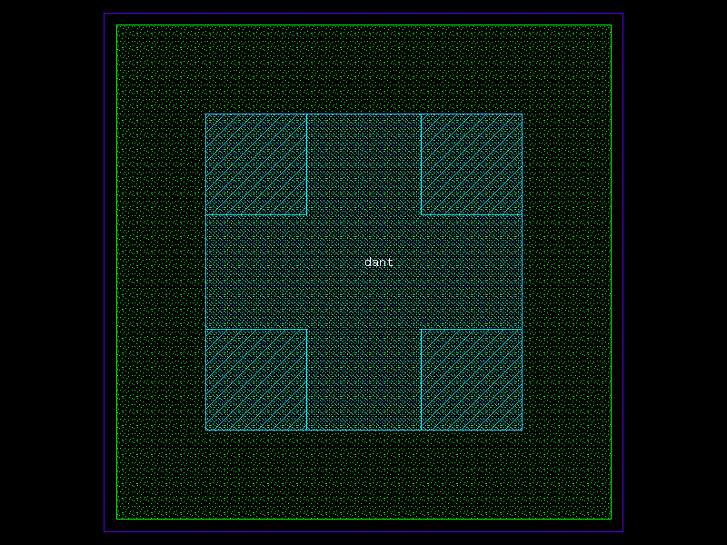
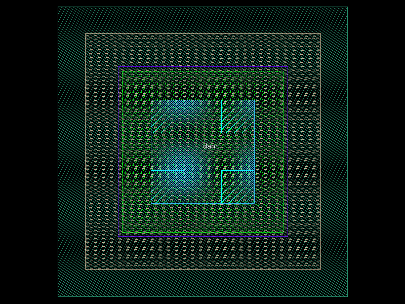
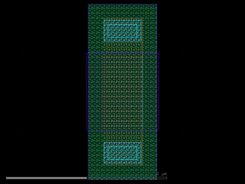
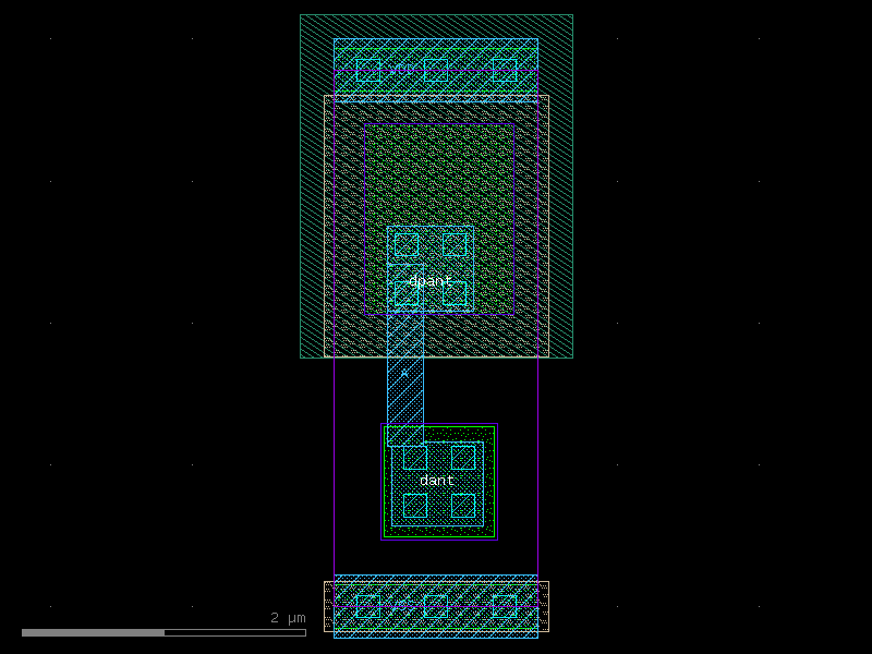
dantenna

Creates a diode antenna (dantenna) structure.

This function generates a layout cell containing a rectangular antenna region with optional recognition layers and guard ring structures. Parameters allow customization of the antenna geometry and the type and spacing of guard rings.

Parameters:

Name Type Description Default
width float

Width of the antenna rectangle in microns.

0.78
length float

Length of the antenna rectangle in microns.

0.78
addRecLayer Literal['t', 'f']

Recognition layer to add (e.g., 'M1' for metal1, 'M2' for metal2, or None for none).

't'
guardRingType Literal['none', 'psub']

Type of guard ring to include. Options include: - 'none': No guard ring - 'psub': P-type guard ring

'none'
guardRingDistance float

Spacing between the antenna body and guard ring in microns.

1.0

Returns:

Type Description
Component

gdsfactory.Component: The generated antenna component.

Raises:

Type Description
ValueError

If width or length is outside allowed range.

Source code in ihp/cells/antennas.py
@gf.cell(schematic_function=dantenna_schematic, tags=["IHP", "diode", "antenna"])
def dantenna(
    width: float = 0.78,
    length: float = 0.78,
    addRecLayer: Literal["t", "f"] = "t",
    guardRingType: Literal["none", "psub"] = "none",
    guardRingDistance: float = 1.0,
) -> gf.Component:
    """Creates a diode antenna (dantenna) structure.

    This function generates a layout cell containing a rectangular antenna
    region with optional recognition layers and guard ring structures.
    Parameters allow customization of the antenna geometry and the type
    and spacing of guard rings.

    Args:
        width: Width of the antenna rectangle in microns.
        length: Length of the antenna rectangle in microns.
        addRecLayer: Recognition layer to add (e.g., 'M1' for metal1, 'M2' for metal2,
            or None for none).
        guardRingType: Type of guard ring to include. Options include:
            - 'none': No guard ring
            - 'psub': P-type guard ring
        guardRingDistance: Spacing between the antenna body and guard ring in microns.

    Returns:
        gdsfactory.Component: The generated antenna component.

    Raises:
        ValueError: If width or length is outside allowed range.
    """
    if width < _TECH.dantenna_min_width or width > _TECH.dantenna_max_width:
        raise ValueError(
            f"dantenna width={width} out of range [{_TECH.dantenna_min_width}, {_TECH.dantenna_max_width}]"
        )
    if length < _TECH.dantenna_min_length or length > _TECH.dantenna_max_length:
        raise ValueError(
            f"dantenna length={length} out of range [{_TECH.dantenna_min_length}, {_TECH.dantenna_max_length}]"
        )

    c = gf.Component()

    layer_metal1: LayerSpec = "Metal1drawing"
    ndiff_layer: LayerSpec = "Activdrawing"
    pdiff_layer: LayerSpec = "Activdrawing"
    pdiffx_layer: LayerSpec = "pSDdrawing"
    cont_layer: LayerSpec = "Contdrawing"
    diods_layer: LayerSpec = "Recogdiode"
    layer_text: LayerSpec = "TEXTdrawing"

    cont_size = _TECH.cont_size
    cont_dist = _TECH.cont_spacing
    cont_diff_over = _TECH.cont_enc_active
    pdiffx_over = _TECH.pSD_a
    diods_over = _TECH.dantenna_dov

    typ = "N"

    x_min, y_min, x_max, y_max = DrawContArray(
        c,
        cont_layer,
        0,
        0,
        width,
        length,
        cont_size,
        cont_dist,
        cont_diff_over,
    )

    # Metal1 encloses the contacts
    metal1_ref = c << gf.components.rectangle(
        size=(x_max - x_min, y_max - y_min), layer=layer_metal1
    )

    metal1_ref.move((x_min, y_min))

    if typ == "N":
        c.add_ref(gf.components.rectangle(size=(width, length), layer=ndiff_layer))
    else:
        c.add_ref(gf.components.rectangle(size=(width, length), layer=pdiff_layer))
        c.add_ref(
            gf.components.rectangle(
                size=(width + 2 * pdiffx_over, length + 2 * pdiffx_over),
                layer=pdiffx_layer,
            )
        ).move((-pdiffx_over, -pdiffx_over))

    c.add_label(
        "dant",
        layer=layer_text,
        position=(
            width / 2,
            length / 2,
        ),
    )

    if addRecLayer == "t":
        c.add_ref(
            gf.components.rectangle(
                size=(width + 2 * diods_over, length + 2 * diods_over),
                layer=diods_layer,
            )
        ).move((-diods_over, -diods_over))

    return c

dantenna

import warnings
warnings.filterwarnings("ignore", category=DeprecationWarning)

from ihp import PDK
from ihp import cells

PDK.activate()

c = cells.dantenna(width=0.78, length=0.78, addRecLayer='t', guardRingType='none', guardRingDistance=1.0).copy()
c.draw_ports()
c.plot()

directional_coupler

Returns a directional coupler coplanar transmission line.

Creates signal and ground lines for a directional coupler.

Parameters:

Name Type Description Default
connection_length float

Length of the input line.

100
frequency float

Operating frequency (Hz).

10000000000.0
coupling_factor float

Coupling factor in dB.

3
signal_cross_section CrossSection | str | dict[str, Any] | Callable[..., CrossSection] | SymmetricalCrossSection | DCrossSection

Cross-section for the signal line.

'topmetal2_routing'
ground_cross_section CrossSection | str | dict[str, Any] | Callable[..., CrossSection] | SymmetricalCrossSection | DCrossSection

Cross-section for the ground line.

'topmetal1_routing'
Z0 float

Target characteristic impedance (ohms).

50
e_r float

Relative permittivity of the substrate. Defaults to 4.1 for silicon dioxide.

4.1
Source code in ihp/cells/rf_devices.py
@gf.cell
def directional_coupler(
    connection_length: float = 100,
    frequency: float = 10e9,
    coupling_factor: float = 3,
    signal_cross_section: CrossSectionSpec = "topmetal2_routing",
    ground_cross_section: CrossSectionSpec = "topmetal1_routing",
    Z0: float = 50,
    e_r: float = 4.1,
) -> gf.Component:
    """Returns a directional coupler coplanar transmission line.

    Creates signal and ground lines for a directional coupler.

    Args:
        connection_length: Length of the input line.
        frequency: Operating frequency (Hz).
        coupling_factor: Coupling factor in dB.
        signal_cross_section: Cross-section for the signal line.
        ground_cross_section: Cross-section for the ground line.
        Z0: Target characteristic impedance (ohms).
        e_r: Relative permittivity of the substrate. Defaults to 4.1 for silicon dioxide.
    """
    wave_length = scipy.constants.c / frequency * 1e6

    c = gf.Component()

    e_eff = _calculate_effective_dielectric_constant(
        signal_cross_section=signal_cross_section,
        ground_cross_section=ground_cross_section,
        e_r=e_r,
    )

    quater_wave_length = wave_length / 4 / sqrt(e_eff)
    quater_wave_length = quater_wave_length - quater_wave_length % (
        tech.nm
    )  # truncate to 5 nm

    # couping factor must be negative
    if coupling_factor > 0:
        coupling_factor = (
            -coupling_factor
        )  # enforce negative coupling factor for the formula below

    coupling_factor_linear = 10 ** (coupling_factor / 20)

    # create the first line of the coupler
    coupled_lines = c.add_ref(
        coupler_tline(
            Z0e=Z0 * (1 + coupling_factor_linear) / (1 - coupling_factor_linear),
            Z0o=Z0 * (1 - coupling_factor_linear) / (1 + coupling_factor_linear),
            length=quater_wave_length,
            signal_cross_section=signal_cross_section,
            ground_cross_section=ground_cross_section,
        )
    )

    # create and connect the input line
    connection_port1 = c.add_ref(
        tline(
            length=connection_length,
            Z0=Z0,
            signal_cross_section=signal_cross_section,
            ground_cross_section=ground_cross_section,
        )
    )
    connection_port1.connect("e1", coupled_lines.ports["e1"])
    # create and connect the through port line
    connection_port2 = c.add_ref(
        tline(
            length=connection_length,
            Z0=Z0,
            signal_cross_section=signal_cross_section,
            ground_cross_section=ground_cross_section,
        )
    )
    connection_port2.connect("e1", coupled_lines.ports["e2"])

    corner_left = c.add_ref(
        tline_corner(
            signal_cross_section=signal_cross_section,
            ground_cross_section=ground_cross_section,
            Z0=Z0,
        )
    )

    corner_left.connect("e1", coupled_lines.ports["e4"])
    connection_port4 = c.add_ref(
        tline(
            length=connection_length,
            Z0=Z0,
            signal_cross_section=signal_cross_section,
            ground_cross_section=ground_cross_section,
        )
    )

    corner_right = c.add_ref(
        tline_corner(
            signal_cross_section=signal_cross_section,
            ground_cross_section=ground_cross_section,
            Z0=Z0,
        )
    )
    connection_port4.connect("e1", corner_left.ports["e2"])

    corner_right.connect("e1", coupled_lines.ports["e3"])
    connection_port3 = c.add_ref(
        tline(
            length=connection_length,
            Z0=Z0,
            signal_cross_section=signal_cross_section,
            ground_cross_section=ground_cross_section,
        )
    )
    connection_port3.connect("e1", corner_right.ports["e4"])

    c.add_port(name="e1", port=connection_port1.ports["e2"])
    c.add_port(name="e2", port=connection_port2.ports["e2"])
    c.add_port(name="e3", port=connection_port3.ports["e2"])
    c.add_port(name="e4", port=connection_port4.ports["e2"])
    c.flatten()
    return c

directional_coupler

import warnings
warnings.filterwarnings("ignore", category=DeprecationWarning)

from ihp import PDK
from ihp import cells

PDK.activate()

c = cells.directional_coupler(connection_length=100, frequency=10000000000.0, coupling_factor=3, signal_cross_section='topmetal2_routing', ground_cross_section='topmetal1_routing', Z0=50, e_r=4.1).copy()
c.draw_ports()
c.plot()

dpantenna

Creates a dual-polarity antenna (dpantenna) structure.

Generates a layout cell containing a rectangular antenna region with an optional recognition layer and an optional n-well guard ring. Parameters allow customization of the antenna geometry and the spacing between the antenna body and the surrounding guard ring.

Parameters:

Name Type Description Default
width float

Width of the antenna rectangle in microns.

0.78
length float

Length of the antenna rectangle in microns.

0.78
addRecLayer Literal['t', 'f']

Whether to add a recognition layer. Valid values: - 't': Add recognition layer. - 'f': Do not add a recognition layer.

't'
guardRingType Literal['none', 'nwell']

Type of guard ring to include. Valid values: - 'none': No guard ring. - 'nwell': Surrounding n-well guard ring.

'none'
guardRingDistance float

Spacing between the antenna body and the n-well guard ring, in microns.

1.0

Returns:

Type Description
Component

gdsfactory.Component: The generated antenna component.

Raises:

Type Description
ValueError

If width or length is outside allowed range.

Source code in ihp/cells/antennas.py
@gf.cell(schematic_function=dpantenna_schematic, tags=["IHP", "diode", "antenna"])
def dpantenna(
    width: float = 0.78,
    length: float = 0.78,
    addRecLayer: Literal["t", "f"] = "t",
    guardRingType: Literal["none", "nwell"] = "none",
    guardRingDistance: float = 1.0,
) -> gf.Component:
    """Creates a dual-polarity antenna (dpantenna) structure.

    Generates a layout cell containing a rectangular antenna region with an
    optional recognition layer and an optional n-well guard ring. Parameters
    allow customization of the antenna geometry and the spacing between the
    antenna body and the surrounding guard ring.

    Args:
        width: Width of the antenna rectangle in microns.
        length: Length of the antenna rectangle in microns.
        addRecLayer: Whether to add a recognition layer. Valid values:
            - 't': Add recognition layer.
            - 'f': Do not add a recognition layer.
        guardRingType: Type of guard ring to include. Valid values:
            - 'none': No guard ring.
            - 'nwell': Surrounding n-well guard ring.
        guardRingDistance: Spacing between the antenna body and the n-well
            guard ring, in microns.

    Returns:
        gdsfactory.Component: The generated antenna component.

    Raises:
        ValueError: If width or length is outside allowed range.
    """
    if width < _TECH.dpantenna_min_width or width > _TECH.dpantenna_max_width:
        raise ValueError(
            f"dpantenna width={width} out of range [{_TECH.dpantenna_min_width}, {_TECH.dpantenna_max_width}]"
        )
    if length < _TECH.dpantenna_min_length or length > _TECH.dpantenna_max_length:
        raise ValueError(
            f"dpantenna length={length} out of range [{_TECH.dpantenna_min_length}, {_TECH.dpantenna_max_length}]"
        )

    c = gf.Component()

    layer_metal1: LayerSpec = "Metal1drawing"
    pdiff_layer: LayerSpec = "Activdrawing"
    pdiffx_layer: LayerSpec = "pSDdrawing"
    cont_layer: LayerSpec = "Contdrawing"
    diods_layer: LayerSpec = "Recogdiode"
    layer_text: LayerSpec = "TEXTdrawing"
    layer_nwell: LayerSpec = "NWelldrawing"

    cont_size = _TECH.cont_size
    cont_dist = _TECH.cont_spacing
    cont_diff_over = _TECH.cont_enc_active
    pdiffx_over = _TECH.psd_activ_over
    diods_over = _TECH.dpantenna_dov
    NW_c = _TECH.nw_activ_over_lv

    x_min, y_min, x_max, y_max = DrawContArray(
        c,
        cont_layer,
        0,
        0,
        width,
        length,
        cont_size,
        cont_dist,
        cont_diff_over,
    )

    # Metal1 encloses the contacts
    metal1_ref = c << gf.components.rectangle(
        size=(x_max - x_min, y_max - y_min), layer=layer_metal1
    )

    metal1_ref.move((x_min, y_min))

    c.add_ref(gf.components.rectangle(size=(width, length), layer=pdiff_layer))
    c.add_ref(
        gf.components.rectangle(
            size=(width + 2 * pdiffx_over, length + 2 * pdiffx_over),
            layer=pdiffx_layer,
        )
    ).move((-pdiffx_over, -pdiffx_over))

    c.add_label(
        "dant",
        layer=layer_text,
        position=(
            width / 2,
            length / 2,
        ),
    )

    if addRecLayer == "t":
        c.add_ref(
            gf.components.rectangle(
                size=(width + 2 * diods_over, length + 2 * diods_over),
                layer=diods_layer,
            )
        ).move((-diods_over, -diods_over))

    c.add_ref(
        gf.components.rectangle(
            size=(width + 2 * NW_c, length + 2 * NW_c),
            layer=layer_nwell,
        )
    ).move((-NW_c, -NW_c))

    return c

dpantenna

import warnings
warnings.filterwarnings("ignore", category=DeprecationWarning)

from ihp import PDK
from ihp import cells

PDK.activate()

c = cells.dpantenna(width=0.78, length=0.78, addRecLayer='t', guardRingType='none', guardRingDistance=1.0).copy()
c.draw_ports()
c.plot()

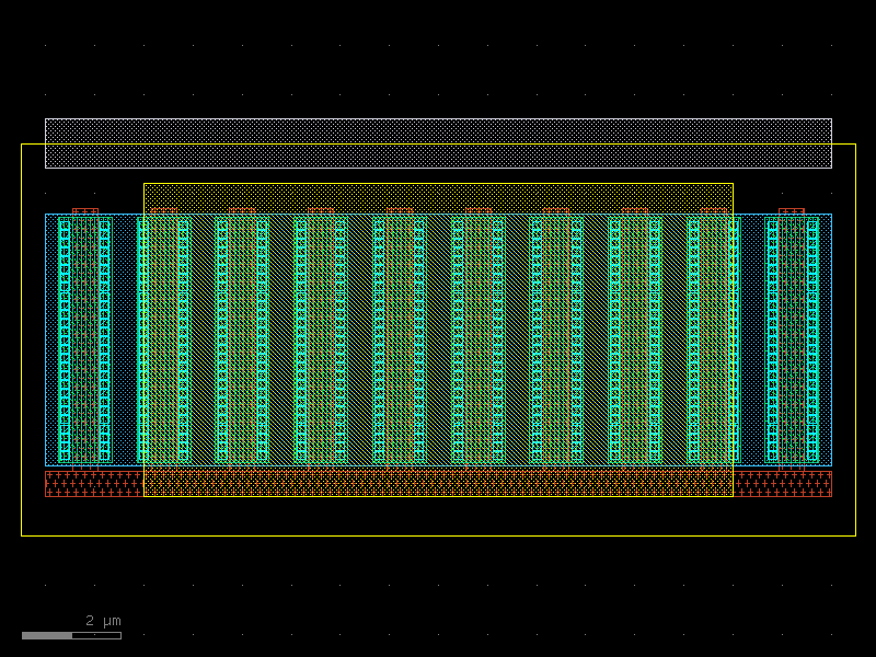
esd_nmos

Create an ESD protection NMOS device.

Parameters:

Name Type Description Default
width float

Total width of the ESD device in micrometers.

50.0
length float

Gate length in micrometers.

0.5
nf int

Number of fingers.

10
model str

Device model name.

'nmoscl_2'
layer_pwell tuple[int, int] | str | int | LayerEnum

P-well layer.

'PWelldrawing'
layer_activ tuple[int, int] | str | int | LayerEnum

Active region layer.

'Activdrawing'
layer_gatpoly tuple[int, int] | str | int | LayerEnum

Gate polysilicon layer.

'GatPolydrawing'
layer_nsd tuple[int, int] | str | int | LayerEnum

N+ source/drain doping layer.

'nSDdrawing'
layer_cont tuple[int, int] | str | int | LayerEnum

Contact layer.

'Contdrawing'
layer_metal1 tuple[int, int] | str | int | LayerEnum

Metal1 layer.

'Metal1drawing'
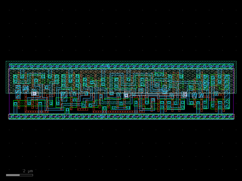
layer_metal2 tuple[int, int] | str | int | LayerEnum

Metal2 layer.

'Metal2drawing'
layer_esd tuple[int, int] | str | int | LayerEnum

ESD marker layer.

'Recogesd'

Returns:

Type Description
Component

Component with ESD NMOS layout.

Source code in ihp/cells/passives.py
@gf.cell(schematic_function=esd_nmos_schematic, tags=["IHP", "esd", "lv"])
def esd_nmos(
    width: float = 50.0,
    length: float = 0.5,
    nf: int = 10,
    model: str = "nmoscl_2",
    layer_pwell: LayerSpec = "PWelldrawing",
    layer_activ: LayerSpec = "Activdrawing",
    layer_gatpoly: LayerSpec = "GatPolydrawing",
    layer_nsd: LayerSpec = "nSDdrawing",
    layer_cont: LayerSpec = "Contdrawing",
    layer_metal1: LayerSpec = "Metal1drawing",
    layer_metal1_pin: LayerSpec = "Metal1pin",
    layer_metal2: LayerSpec = "Metal2drawing",
    layer_metal2_pin: LayerSpec = "Metal2pin",
    layer_esd: LayerSpec = "Recogesd",
) -> Component:
    """Create an ESD protection NMOS device.

    Args:
        width: Total width of the ESD device in micrometers.
        length: Gate length in micrometers.
        nf: Number of fingers.
        model: Device model name.
        layer_pwell: P-well layer.
        layer_activ: Active region layer.
        layer_gatpoly: Gate polysilicon layer.
        layer_nsd: N+ source/drain doping layer.
        layer_cont: Contact layer.
        layer_metal1: Metal1 layer.
        layer_metal2: Metal2 layer.
        layer_esd: ESD marker layer.

    Returns:
        Component with ESD NMOS layout.
    """
    c = Component()

    # Design rules for ESD devices
    gate_width = width / nf
    gate_length = length
    gate_ext = 0.18
    active_ext = 0.3  # Larger for ESD
    cont_size = 0.16
    cont_spacing = 0.18
    cont_enc = 0.07
    metal_enc = 0.06
    pwell_enc = 0.5

    # Grid snap
    grid = 0.005
    gate_width = round(gate_width / grid) * grid
    gate_length = round(gate_length / grid) * grid

    # P-Well for ESD NMOS
    pwell = gf.components.rectangle(
        size=(
            (gate_length + 2 * active_ext) * nf + pwell_enc * 2,
            gate_width + 2 * gate_ext + pwell_enc * 2,
        ),
        layer=layer_pwell,
        centered=True,
    )
    c.add_ref(pwell)

    # Create multi-finger ESD structure
    finger_pitch = gate_length + 2 * active_ext + 0.5

    for i in range(nf):
        x_offset = (i - nf / 2 + 0.5) * finger_pitch

        # Gate poly
        gate = gf.components.rectangle(
            size=(gate_length, gate_width + 2 * gate_ext),
            layer=layer_gatpoly,
        )
        gate_ref = c.add_ref(gate)
        gate_ref.move((x_offset - gate_length / 2, -gate_width / 2 - gate_ext))

        # Active region
        active = gf.components.rectangle(
            size=(gate_length + 2 * active_ext, gate_width),
            layer=layer_activ,
        )
        active_ref = c.add_ref(active)
        active_ref.move((x_offset - gate_length / 2 - active_ext, -gate_width / 2))

        # N+ implant
        nsd = gf.components.rectangle(
            size=(gate_length + 2 * active_ext, gate_width),
            layer=layer_nsd,
        )
        nsd_ref = c.add_ref(nsd)
        nsd_ref.move((x_offset - gate_length / 2 - active_ext, -gate_width / 2))

        # Source/Drain contacts
        n_cont_y = int((gate_width - cont_size) / cont_spacing) + 1

        for j in range(n_cont_y):
            y_pos = -gate_width / 2 + cont_enc + j * cont_spacing

            # Source contact
            cont_s = gf.components.rectangle(
                size=(cont_size, cont_size),
                layer=layer_cont,
            )
            cont_s_ref = c.add_ref(cont_s)
            cont_s_ref.move((x_offset - gate_length / 2 - active_ext + cont_enc, y_pos))

            # Drain contact
            cont_d = gf.components.rectangle(
                size=(cont_size, cont_size),
                layer=layer_cont,
            )
            cont_d_ref = c.add_ref(cont_d)
            cont_d_ref.move((x_offset + gate_length / 2 + cont_enc, y_pos))

    # Metal bus connections
    # Source bus (connected to ground)
    source_bus = gf.components.rectangle(
        size=(nf * finger_pitch, gate_width + 2 * metal_enc),
        layer=layer_metal1,
    )
    source_bus_ref = c.add_ref(source_bus)
    source_bus_ref.move((-nf * finger_pitch / 2, -gate_width / 2 - metal_enc))

    # Drain bus (connected to I/O pad)
    drain_bus = gf.components.rectangle(
        size=(nf * finger_pitch, 1.0),
        layer=layer_metal2,
    )
    drain_bus_ref = c.add_ref(drain_bus)
    drain_bus_ref.move((-nf * finger_pitch / 2, gate_width / 2 + 1.0))

    # Gate bus (can be tied to source or left floating)
    gate_bus = gf.components.rectangle(
        size=(nf * finger_pitch, 0.5),
        layer=layer_gatpoly,
    )
    gate_bus_ref = c.add_ref(gate_bus)
    gate_bus_ref.move((-nf * finger_pitch / 2, -gate_width / 2 - gate_ext - 0.5))

    # ESD marker
    esd_mark = gf.components.rectangle(
        size=(nf * finger_pitch + 1.0, gate_width + 3.0),
        layer=layer_esd,
        centered=True,
    )
    c.add_ref(esd_mark)

    # Add ports
    c.add_port(
        name="PAD",
        center=(0, gate_width / 2 + 1.5),
        width=nf * finger_pitch,
        orientation=90,
        layer=layer_metal2_pin,
        port_type="electrical",
    )

    c.add_port(
        name="GND",
        center=(0, -gate_width / 2),
        width=nf * finger_pitch,
        orientation=270,
        layer=layer_metal1_pin,
        port_type="electrical",
    )

    return c

esd_nmos

import warnings
warnings.filterwarnings("ignore", category=DeprecationWarning)

from ihp import PDK
from ihp import cells

PDK.activate()

c = cells.esd_nmos(width=50.0, length=0.5, nf=10, model='nmoscl_2', layer_pwell='PWelldrawing', layer_activ='Activdrawing', layer_gatpoly='GatPolydrawing', layer_nsd='nSDdrawing', layer_cont='Contdrawing', layer_metal1='Metal1drawing', layer_metal1_pin='Metal1pin', layer_metal2='Metal2drawing', layer_metal2_pin='Metal2pin', layer_esd='Recogesd').copy()
c.draw_ports()
c.plot()

guard_ring

Create an N-Well (NW) and N-Plus (NP) or a P-Plus (PP) guard ring around a boundary box, or, if bbox is not provided, along a provided path of points.

Parameters:

Name Type Description Default
width float

Width of the guard ring group path, defining the width of the Metal1 Path.

0.5
guardRingSpacing float

Spacing between the Metal1 Path and the component BBox.

0.14
guardRingType Literal['psub', 'nwell']

Literal["psub", 'nwell'] Type of Guard-Ring (NP = nwell or PP = psub).

'psub'
bbox tuple[Point, Point] | None

Encapsulated component bounding box.

((-5, -5), (5, 5))
path list[tuple[Point, Point]] | None

Path point for the group path defining the Guard Ring,

None
layer_activ tuple[int, int] | str | int | LayerEnum

Activ drawing layer.

'Activdrawing'
layer_cont tuple[int, int] | str | int | LayerEnum

Contact Via drawing layer.

'Contdrawing'
layer_metal1 tuple[int, int] | str | int | LayerEnum

Metal1 drawing layer.

'Metal1drawing'
layer_psd tuple[int, int] | str | int | LayerEnum

pSD / P-Plus drawing layer.

'pSDdrawing'
layer_nwell tuple[int, int] | str | int | LayerEnum

NWell drawing layer.

'NWelldrawing'
layer_nsd tuple[int, int] | str | int | LayerEnum

nSD / N-Plus drawing layer.

'nSDdrawing'

Returns: c - Component containing the Guard-Ring group path. Raises:

Source code in ihp/cells/passives.py
@gf.cell(tags=["IHP", "guardring"])
def guard_ring(
    width: float = 0.5,
    guardRingSpacing: float = 0.14,
    guardRingType: Literal["psub", "nwell"] = "psub",
    bbox: tuple[Point, Point] | None = ((-5, -5), (5, 5)),
    path: list[tuple[Point, Point]] | None = None,
    layer_activ: LayerSpec = "Activdrawing",
    layer_cont: LayerSpec = "Contdrawing",
    layer_metal1: LayerSpec = "Metal1drawing",
    layer_psd: LayerSpec = "pSDdrawing",
    layer_nwell: LayerSpec = "NWelldrawing",
    layer_nsd: LayerSpec = "nSDdrawing",
    **kwargs,
) -> Component:
    """
    Create an N-Well (NW) and N-Plus (NP) or a P-Plus (PP)
    guard ring around a boundary box, or, if `bbox` is not provided,
    along a provided `path` of points.

    Args:
        width: Width of the guard ring group path,
            defining the width of the Metal1 Path.
        guardRingSpacing: Spacing between the Metal1 Path and the component BBox.
        guardRingType: Literal["psub", 'nwell'] Type of Guard-Ring (NP = nwell or PP = psub).
        bbox: Encapsulated component bounding box.
        path: Path point for the group path defining the Guard Ring,
        layer_activ: Activ drawing layer.
        layer_cont: Contact Via drawing layer.
        layer_metal1: Metal1 drawing layer.
        layer_psd: pSD / P-Plus drawing layer.
        layer_nwell: NWell drawing layer.
        layer_nsd: nSD / N-Plus drawing layer.
    Returns:
        c - Component containing the Guard-Ring group path.
    Raises:
    """

    gr_drc = {
        # metals
        "m1_min_width": tech.TECH.metal1_width,
        # active regions and contact
        "cont_min_size": tech.TECH.cont_size,
        "cont_min_spacing": tech.TECH.cont_spacing,
        "cont_min_enclose_active": tech.TECH.cont_enc_active,
        "cont_min_enclose_metal": tech.TECH.cont_enc_metal,
        # TODO: add in the original tech struct
        "active_min_enclose_np": 0.14,
        "active_min_enclose_pp": 0.14,
        "np_min_enclose_nw": 0.14,
    }

    min_width = gr_drc["cont_min_size"] + 2 * max(
        gr_drc["cont_min_enclose_active"], gr_drc["cont_min_enclose_metal"]
    )
    min_width = max(min_width, gr_drc["m1_min_width"])
    assert width >= min_width, (
        f"Guard Ring width >= {min_width} to comply with Min cont enclosure and metal width"
    )

    # define nrows and ncols of the required tap
    nrows = int(floor(width / min_width))
    c = Component()

    # define the path
    if bbox is not None:
        path = [
            (
                bbox[0][0] - guardRingSpacing - width / 2,
                bbox[1][1] + guardRingSpacing + width / 2,
            ),
            (
                bbox[1][0] + guardRingSpacing + width / 2,
                bbox[1][1] + guardRingSpacing + width / 2,
            ),
            (
                bbox[1][0] + guardRingSpacing + width / 2,
                bbox[0][1] - guardRingSpacing - width / 2,
            ),
            (
                bbox[0][0] - guardRingSpacing - width / 2,
                bbox[0][1] - guardRingSpacing - width / 2,
            ),
            (
                bbox[0][0] - guardRingSpacing - width / 2,
                bbox[1][1] + guardRingSpacing + width,
            ),
        ]
        enclosure = max(
            gr_drc["cont_min_enclose_active"], gr_drc["cont_min_enclose_metal"]
        )
        cont_path = [
            (
                bbox[0][0] - guardRingSpacing - enclosure,
                bbox[1][1] + guardRingSpacing + enclosure,
            ),
            (
                bbox[1][0] + guardRingSpacing + enclosure,
                bbox[1][1] + guardRingSpacing + enclosure,
            ),
            (
                bbox[1][0] + guardRingSpacing + enclosure,
                bbox[0][1] - guardRingSpacing - enclosure,
            ),
            (
                bbox[0][0] - guardRingSpacing - enclosure,
                bbox[0][1] - guardRingSpacing - enclosure,
            ),
            (bbox[0][0] - guardRingSpacing - enclosure, bbox[1][1] + guardRingSpacing),
        ]

    assert path is not None, "Neither path or bbox was provided."
    # place taps around path
    tap_layers = [layer_activ, layer_metal1]
    main = None
    for layer_spec in tap_layers:
        p = gf.path.extrude(gf.path.Path(path), width=width, layer=layer_spec)
        main = c.add_ref(p)
    if guardRingType == "psub":
        sep = gr_drc["active_min_enclose_pp"]
        last_point = list(path[-1])
        last_edge = (path[-1][0] - path[-2][0], path[-1][1] - path[-2][1])
        norm = np.linalg.norm(last_edge)
        dir_vec = np.array(last_edge) / norm
        # manhattan
        dir_vec[0] = round(dir_vec[0])
        dir_vec[1] = round(dir_vec[1])
        last_point[0] += sep * dir_vec[0]
        last_point[1] += sep * dir_vec[1]
        new_path = path.copy()
        new_path[-1] = tuple(last_point)
        p = gf.path.extrude(
            gf.path.Path(new_path), width=width + 2 * sep, layer=layer_psd
        )
        c.add_ref(p)
    if guardRingType == "nwell":
        sep = gr_drc["active_min_enclose_np"]
        last_point = list(path[-1])
        last_edge = (path[-1][0] - path[-2][0], path[-1][1] - path[-2][1])
        norm = np.linalg.norm(last_edge)
        dir_vec = np.array(last_edge) / norm
        # manhattan
        dir_vec[0] = round(dir_vec[0])
        dir_vec[1] = round(dir_vec[1])
        last_point[0] += sep * dir_vec[0]
        last_point[1] += sep * dir_vec[1]
        new_path = path.copy()
        new_path[-1] = tuple(last_point)
        p = gf.path.extrude(
            gf.path.Path(new_path), width=width + 2 * sep, layer=layer_nsd
        )

        sep += gr_drc["np_min_enclose_nw"]
        last_point = list(path[-1])
        last_point[0] += sep * dir_vec[0]
        last_point[1] += sep * dir_vec[1]
        new_path = path.copy()
        new_path[-1] = tuple(last_point)
        nwl = gf.path.extrude(
            gf.path.Path(new_path), width=width + 2 * sep, layer=layer_nwell
        )
        c.add_ref(p)
        c.add_ref(nwl)

    cont_tap = cells.via_array(
        via_type=layer_cont.split("drawing")[0],
        via_size=gr_drc["cont_min_size"],
        via_spacing=gr_drc["cont_min_size"] + gr_drc["cont_min_spacing"],
        via_enclosure=gr_drc["cont_min_enclose_active"],
        columns=1,
        rows=nrows,
    )

    conts = gf.path.along_path(
        gf.path.Path(cont_path if bbox is not None else path),
        cont_tap,
        gr_drc["cont_min_spacing"] + gr_drc["cont_min_size"],
        0.0,
    )
    cont_ref = c.add_ref(conts)
    cont_ref.x = main.x
    cont_ref.y = main.y
    c.info["model"] = f"{guardRingType}-guard-ring"
    c.info["width"] = width
    c.info["rows"] = nrows
    c.info["guardRingSpacing"] = guardRingSpacing

    return c

guard_ring

import warnings
warnings.filterwarnings("ignore", category=DeprecationWarning)

from ihp import PDK
from ihp import cells

PDK.activate()

c = cells.guard_ring(width=0.5, guardRingSpacing=0.14, guardRingType='psub', bbox=((-5, -5), (5, 5)), layer_activ='Activdrawing', layer_cont='Contdrawing', layer_metal1='Metal1drawing', layer_psd='pSDdrawing', layer_nwell='NWelldrawing', layer_nsd='nSDdrawing').copy()
c.draw_ports()
c.plot()

hairpin_coupled_line_bandpass_filter

Return a hairpin-coupled-line bandpass filter.

Synthesizes an N-th order hairpin-coupled-line bandpass filter from prototype coefficients and maps it into coupled-line sections.

Parameters:

Name Type Description Default
order int

Filter order.

3
frequency float

Center frequency in Hz.

10000000000.0
bandwidth float

Absolute bandwidth in Hz.

1000000000.0
connection_length float

Length of the input/output feed line in um.

50
Z0 float

Port impedance in ohms.

50
signal_cross_section CrossSection | str | dict[str, Any] | Callable[..., CrossSection] | SymmetricalCrossSection | DCrossSection

Cross-section for signal routing.

'topmetal2_routing'
ground_cross_section CrossSection | str | dict[str, Any] | Callable[..., CrossSection] | SymmetricalCrossSection | DCrossSection

Cross-section for ground routing.

'topmetal1_routing'
e_r float

Relative permittivity used for synthesis.

4.1
filter_type str

Prototype family, either butter or cheby.

'butter'
ripple_dB float

Chebyshev passband ripple in dB (used when filter_type='cheby').

3

Returns:

Type Description
Component

A parametric hairpin bandpass filter component.

Source code in ihp/cells/rf_devices.py
@gf.cell
def hairpin_coupled_line_bandpass_filter(
    order: int = 3,
    frequency: float = 10e9,
    bandwidth: float = 1e9,
    connection_length: float = 50,
    Z0: float = 50,
    signal_cross_section: CrossSectionSpec = "topmetal2_routing",
    ground_cross_section: CrossSectionSpec = "topmetal1_routing",
    e_r: float = 4.1,
    filter_type: str = "butter",
    ripple_dB: float = 3,
) -> gf.Component:
    """Return a hairpin-coupled-line bandpass filter.

    Synthesizes an N-th order hairpin-coupled-line bandpass filter from
    prototype coefficients and maps it into coupled-line sections.

    Args:
        order: Filter order.
        frequency: Center frequency in Hz.
        bandwidth: Absolute bandwidth in Hz.
        connection_length: Length of the input/output feed line in um.
        Z0: Port impedance in ohms.
        signal_cross_section: Cross-section for signal routing.
        ground_cross_section: Cross-section for ground routing.
        e_r: Relative permittivity used for synthesis.
        filter_type: Prototype family, either ``butter`` or ``cheby``.
        ripple_dB: Chebyshev passband ripple in dB (used when
            ``filter_type='cheby'``).

    Returns:
        A parametric hairpin bandpass filter component.
    """

    c = gf.Component()
    # get filter coefficients
    # g = [g1 g2 ... gN gN+1] for N-th order filter
    if filter_type == "butter":
        g = _butterworth_prototype(order)
    elif filter_type == "cheby":
        g = _chebyshev_prototype(order, ripple_dB)

    fractional_bandwidth = bandwidth / frequency
    f_2 = frequency * (1 + fractional_bandwidth / 2)
    f_1 = frequency * (1 - fractional_bandwidth / 2)

    delta = fractional_bandwidth

    # initialize lists for Z0J values
    Z0J = [0.0] * (order + 1)

    # first Z0J value
    Z0J[0] = sqrt(pi * delta / (2 * g[0]))

    # calculate Z0J values for j = 1 to N-1
    for j in range(1, order):
        Z0J[j] = pi * delta / (2 * sqrt(g[j - 1] * g[j]))

    # last Z0J value
    Z0J[order] = sqrt(pi * delta / (2 * g[order - 1] * g[order]))

    # initialize and calculate Z0e and Z0o values for each section
    Z0e = [0.0] * (order + 1)
    Z0o = [0.0] * (order + 1)
    Z_section = [0.0] * (order + 1)

    for j in range(order + 1):
        Z0e[j] = Z0 * (1 + Z0J[j] + Z0J[j] ** 2)
        Z0o[j] = Z0 * (1 - Z0J[j] + Z0J[j] ** 2)

        Z_section[j] = sqrt(Z0e[j] * Z0o[j])

    # calculate the coupling coefficient k for each section
    g = [1.0] + g  # prepend g0 = 1.0 for easier indexing
    k = [0.0] * (order + 1)
    for j in range(order + 1):
        k[j] = (f_2 - f_1) / sqrt(f_1 * f_2 * g[j] * g[j + 1])

    e_eff = _calculate_effective_dielectric_constant(
        signal_cross_section=signal_cross_section,
        ground_cross_section=ground_cross_section,
        e_r=e_r,
    )

    width_Z0 = _calculate_width_from_Z0(
        Z0=Z0,
        ground_cross_section=ground_cross_section,
        signal_cross_section=signal_cross_section,
        e_r=e_r,
    )

    segment_length = scipy.constants.c / frequency * 1e6 / sqrt(e_eff) / 4
    segment_length = segment_length - segment_length % tech.nm  # snap to grid

    input_line = c.add_ref(
        tline(
            length=connection_length,
            signal_cross_section=signal_cross_section,
            ground_cross_section=ground_cross_section,
            Z0=Z0,
        )
    )

    first_vertical_line = tline(
        length=segment_length
        - 2 * width_Z0,  # adjust length to account for the port at the end
        signal_cross_section=signal_cross_section,
        ground_cross_section=ground_cross_section,
        Z0=Z0,
    ).copy()
    # copy to be able to add port

    # from Microstrip Filters for RF/Microwave Applications by Jia-Sheng Hong, M. J. Lancaster
    t = (
        2
        * segment_length
        / scipy.constants.pi
        * asin(sqrt((fractional_bandwidth) / (g[1])))
    )

    first_vertical_line.add_port(
        name="e3",
        center=(segment_length - t, -width_Z0 / 2),
        width=width_Z0,
        orientation=270,
        port_type="electrical",
        layer=gf.get_cross_section(signal_cross_section).layer,
    )

    first_vertical_line_ref = c.add_ref(first_vertical_line)

    first_vertical_line_ref.connect("e3", input_line.ports["e2"])

    previous_line_ref = first_vertical_line_ref

    for i in range(order + 1):
        section_i = c.add_ref(
            coupler_tline(
                Z0e=Z0e[i],
                Z0o=Z0o[i],
                length=segment_length
                - 2 * width_Z0,  # adjust length to account for the port at the end
                signal_cross_section=signal_cross_section,
                ground_cross_section=ground_cross_section,
            )
        )
        corner_l = c.add_ref(
            _corner_rectangle(
                width=width_Z0,
                length=previous_line_ref.ports["e3"].width,
                cross_section=signal_cross_section,
            )
        )

        connection_i = c.add_ref(
            tline(
                length=previous_line_ref.ports["e2"].width
                + section_i.ports[
                    "e3"
                ].width,  # arbitrary length to connect the horizontal line to the coupler, can be adjusted for better performance
                signal_cross_section=signal_cross_section,
                ground_cross_section=ground_cross_section,
                Z0=Z0,
            )
        )

        corner_r = c.add_ref(
            _corner_rectangle(
                width=width_Z0,
                length=section_i.ports["e3"].width,
                cross_section=signal_cross_section,
            )
        )

        if i % 2 == 0:
            corner_l.connect("e1", previous_line_ref.ports["e2"])
            connection_i.connect("e1", corner_l.ports["e2"])
            corner_r.connect("e4", connection_i.ports["e2"])

            section_i.connect("e3", corner_r.ports["e1"])
        else:
            corner_l.connect("e3", previous_line_ref.ports["e1"])
            connection_i.connect("e1", corner_l.ports["e2"])
            corner_r.connect("e4", connection_i.ports["e2"])

            section_i.connect("e4", corner_r.ports["e3"])

        previous_line_ref = section_i

    corner_l = c.add_ref(
        _corner_rectangle(
            width=width_Z0,
            length=previous_line_ref.ports["e3"].width,
            cross_section=signal_cross_section,
        )
    )

    connection_i = c.add_ref(
        tline(
            length=previous_line_ref.ports["e2"].width
            + width_Z0,  # arbitrary length to connect the horizontal line to the coupler, can be adjusted for better performance
            signal_cross_section=signal_cross_section,
            ground_cross_section=ground_cross_section,
            Z0=Z0,
        )
    )

    corner_r = c.add_ref(
        _corner_rectangle(
            width=width_Z0,
            length=width_Z0,
            cross_section=signal_cross_section,
        )
    )

    last_vertical_line_ref = c.add_ref(first_vertical_line)

    output_line = c.add_ref(
        tline(
            length=connection_length,
            signal_cross_section=signal_cross_section,
            ground_cross_section=ground_cross_section,
            Z0=Z0,
        )
    )

    if order % 2 == 1:
        last_vertical_line_ref.mirror()
        corner_l.connect("e1", previous_line_ref.ports["e2"])
        connection_i.connect("e1", corner_l.ports["e2"])
        corner_r.connect("e4", connection_i.ports["e2"])
        last_vertical_line_ref.connect("e2", corner_r.ports["e1"])

        output_line.connect("e1", last_vertical_line_ref.ports["e3"])
    else:
        corner_l.connect("e3", previous_line_ref.ports["e1"])
        connection_i.connect("e1", corner_l.ports["e2"])
        corner_r.connect("e4", connection_i.ports["e2"])

        last_vertical_line_ref.connect("e2", corner_r.ports["e3"])

        output_line.connect("e1", last_vertical_line_ref.ports["e3"])

    c.add_port(name="e1", port=input_line.ports["e1"])
    c.add_port(name="e2", port=output_line.ports["e2"])

    # c.add_port(name="e1", port=input_line.ports["e1"])

    return c

hairpin_coupled_line_bandpass_filter

import warnings
warnings.filterwarnings("ignore", category=DeprecationWarning)

from ihp import PDK
from ihp import cells

PDK.activate()

c = cells.hairpin_coupled_line_bandpass_filter(order=3, frequency=10000000000.0, bandwidth=1000000000.0, connection_length=50, Z0=50, signal_cross_section='topmetal2_routing', ground_cross_section='topmetal1_routing', e_r=4.1, filter_type='butter', ripple_dB=3).copy()
c.draw_ports()
c.plot()

inductor2

Create a 2-turn inductor.

Parameters:

Name Type Description Default
width float

Width of the inductor trace in micrometers.

2.0
space float

Space between turns in micrometers.

2.1
diameter float

Inner diameter in micrometers.

25.35
vias_width float

Width of vias in micrometers (only when turns > 2)

0.9
resistance float

Resistance in ohms.

0.5777
inductance float

Inductance in henries.

3.3303e-11
terminal_1_length float

Length of the shorter terminal

30.0
turns int

Number of turns (default 1 for inductor2).

1

Returns:

Type Description
Component

Component with inductor layout.

Source code in ihp/cells/inductors.py
@gf.cell(tags=["IHP", "inductor"])
def inductor2(
    width: float = 2.0,
    space: float = 2.1,
    diameter: float = 25.35,
    vias_width: float = 0.9,
    resistance: float = 0.5777,
    inductance: float = 33.303e-12,
    terminal_1_length: float = 30.0,
    turns: int = 1,
    layer_metal_1: LayerSpec = "TopMetal1drawing",
    layer_metal_2: LayerSpec = "TopMetal2drawing",
    layer_inductor: LayerSpec = "INDdrawing",
    layer_metal_1_pin: LayerSpec = "TopMetal1pin",
    layer_metal_2_pin: LayerSpec = "TopMetal2pin",
    layer_ind_pin: LayerSpec = "INDpin",
    layer_via: LayerSpec = "TopVia2drawing",
    layers_no_fill: LayerSpecs = (
        "Activnofill",
        "GatPolynofill",
        "Metal1nofill",
        "Metal2nofill",
        "Metal3nofill",
        "Metal4nofill",
        "Metal5nofill",
        "TopMetal1nofill",
        "TopMetal2nofill",
        "PWellblock",
        "NoRCXdrawing",
    ),
) -> Component:
    """Create a 2-turn inductor.

    Args:
        width: Width of the inductor trace in micrometers.
        space: Space between turns in micrometers.
        diameter: Inner diameter in micrometers.
        vias_width: Width of vias in micrometers (only when turns > 2)
        resistance: Resistance in ohms.
        inductance: Inductance in henries.
        terminal_1_length: Length of the shorter terminal
        turns: Number of turns (default 1 for inductor2).

    Returns:
        Component with inductor layout.
    """
    if not isinstance(turns, int) or turns < 1:
        raise ValueError("turns must be an integer >= 1")

    c = Component()

    Pin_layers_1 = [layer_metal_1_pin, layer_ind_pin]
    Pin_layers_2 = [layer_metal_2_pin, layer_ind_pin]

    w = snap_to_grid(width, grid=0.005 * 2)
    s = snap_to_grid(space)
    d = snap_to_grid(diameter, grid=0.005 * 2)

    apothem_innermost = d / 2
    vertex_angle = math.pi / 4.0  # 45°
    half_vertex_angle = vertex_angle / 2  # 22.5°

    length_short_terminal = terminal_1_length
    length_long_terminal = length_short_terminal + w + (w + s) * (turns - 1)

    octagon_center_offset_y = length_long_terminal + apothem_innermost

    # Add inductor layer
    outer_polygon_pts = []
    for i in range(8):
        r_outer = octagon_center_offset_y / math.cos(half_vertex_angle)
        angle = i * vertex_angle + half_vertex_angle

        x = snap_to_grid(r_outer * math.cos(angle))
        y = snap_to_grid(r_outer * math.sin(angle) + octagon_center_offset_y)
        outer_polygon_pts.append((x, y))
    c.add_polygon(points=outer_polygon_pts, layer=layer_inductor)

    # Add No fill layers
    for layer in layers_no_fill:
        c.add_polygon(points=outer_polygon_pts, layer=layer)

    # Handle the terminals and pins of the inductor
    if turns == 1:
        port1_single_turn = c << gf.components.rectangle(
            size=(w, length_short_terminal + w), layer=layer_metal_2
        )
        port1_single_turn.move((-w - s / 2, 0))
        c.add_port(
            name="P1",
            center=(-w / 2 - s / 2, 0),
            width=w,
            orientation=270,
            layer=layer_metal_2_pin,
            port_type="electrical",
        )

        for layer in Pin_layers_2:
            pin_1_trace = c << gf.components.rectangle(size=(w, w), layer=layer)
            pin_1_trace.move((-w - s / 2, 0))

        port2_single_turn = c << gf.components.rectangle(
            size=(w, length_short_terminal + w), layer=layer_metal_2
        )
        port2_single_turn.move((s / 2, 0))
        c.add_port(
            name="P2",
            center=(w / 2 + s / 2, 0),
            width=w,
            orientation=270,
            layer=layer_metal_2_pin,
            port_type="electrical",
        )

        for layer in Pin_layers_2:
            pin_2_trace = c << gf.components.rectangle(size=(w, w), layer=layer)
            pin_2_trace.move((s / 2, 0))
    else:
        port_short = c << gf.components.rectangle(
            size=(w, length_short_terminal), layer=layer_metal_2
        )
        port_short.move((-w / 2, 0))
        c.add_port(
            name="P1",
            center=(0, 0),
            width=w,
            orientation=270,
            layer=layer_metal_2_pin,
            port_type="electrical",
        )

        for layer in Pin_layers_2:
            pin_short_trace = c << gf.components.rectangle(size=(w, w), layer=layer)
            pin_short_trace.move((-w / 2, 0))

        port_long_1 = c << gf.components.rectangle(
            size=(w, length_long_terminal), layer=layer_metal_1
        )
        port_long_1.move((-(w + s) - w / 2, 0))
        c.add_port(
            name="P2",
            center=(-(w + s), 0),
            width=w,
            orientation=270,
            layer=layer_metal_1_pin,
            port_type="electrical",
        )

        for layer in Pin_layers_1:
            pin_long1_trace = c << gf.components.rectangle(size=(w, w), layer=layer)
            pin_long1_trace.move((-(w + s) - w / 2, 0))

        port_long_2 = c << gf.components.rectangle(
            size=(w, length_long_terminal), layer=layer_metal_1
        )
        port_long_2.move(((w + s) - w / 2, 0))
        c.add_port(
            name="P3",
            center=(w + s, 0),
            width=w,
            orientation=270,
            layer=layer_metal_1_pin,
            port_type="electrical",
        )

        for layer in Pin_layers_1:
            pin_long1_trace = c << gf.components.rectangle(size=(w, w), layer=layer)
            pin_long1_trace.move((w + s - w / 2, 0))

    # We break down the body of inductor into 3 sections
    for k in range(turns):
        apothem = (apothem_innermost + w / 2) + (w + s) * k
        half_octagon_side = apothem * math.tan(half_vertex_angle)

        # Step 1a: We handle the left semi-octagon loops
        x = (-s / 2) if turns == 1 else (-s - w / 2)
        left_octagon_fragment = [
            (x, octagon_center_offset_y + apothem),
            (-half_octagon_side, octagon_center_offset_y + apothem),
            (-apothem, octagon_center_offset_y + half_octagon_side),
            (-apothem, octagon_center_offset_y - half_octagon_side),
            (-half_octagon_side, octagon_center_offset_y - apothem),
            (x, octagon_center_offset_y - apothem),
        ]

        left_path = gf.Path(left_octagon_fragment)
        _ = c << gf.path.extrude(left_path, layer=layer_metal_2, width=w)

        # Step 1b: We handle the right semi-octagon loops
        x = (s / 2) if turns == 1 else (s + w / 2)
        right_octagon_fragment = [
            (x, octagon_center_offset_y + apothem),
            (half_octagon_side, octagon_center_offset_y + apothem),
            (apothem, octagon_center_offset_y + half_octagon_side),
            (apothem, octagon_center_offset_y - half_octagon_side),
            (half_octagon_side, octagon_center_offset_y - apothem),
            (x, octagon_center_offset_y - apothem),
        ]

        right_path = gf.Path(right_octagon_fragment)
        _ = c << gf.path.extrude(right_path, layer=layer_metal_2, width=w)

        # Step 2: We handle the connections of the loops within TM2
        if turns == 1:
            center_fragment = [
                (-w - s / 2, octagon_center_offset_y + apothem),
                (w + s / 2, octagon_center_offset_y + apothem),
            ]
            center_path = gf.Path(center_fragment)
            _ = c << gf.path.extrude(center_path, layer=layer_metal_2, width=w)
        else:
            if k == 0:
                continue

            center_fragment = [
                (-s - w / 2, octagon_center_offset_y - apothem),
                (s + w / 2, octagon_center_offset_y - apothem),
            ]
            center_path = gf.Path(center_fragment)
            c << gf.path.extrude(center_path, layer=layer_metal_2, width=w)

            connecting_fragment_TM2 = [
                (-s - w / 2, octagon_center_offset_y + apothem - w - s),
                (-w, octagon_center_offset_y + apothem - w - s),
                (w, octagon_center_offset_y + apothem),
                (s + w / 2, octagon_center_offset_y + apothem),
            ]

            connecting_path_TM2 = gf.Path(connecting_fragment_TM2)
            c << gf.path.extrude(connecting_path_TM2, layer=layer_metal_2, width=w)

    # Step 3: We handle the cross connection of the loops using TM1 and vias
    if turns > 1:
        connecting_fragment_TM1 = [
            (-s - w / 2 - w, octagon_center_offset_y + apothem),
            (-w, octagon_center_offset_y + apothem),
            (w, octagon_center_offset_y + apothem - (w + s) * (turns - 1)),
            (s + w / 2 + w, octagon_center_offset_y + apothem - (w + s) * (turns - 1)),
        ]
        connecting_path_TM1 = gf.Path(connecting_fragment_TM1)
        c << gf.path.extrude(connecting_path_TM1, layer=layer_metal_1, width=w)

        offset_x = w / 2 - vias_width / 2
        offset_y = vias_width / 2

        via_1_trace = c << gf.components.rectangle(
            size=(vias_width, vias_width), layer=layer_via
        )
        via_1_trace.move(
            (-s - w / 2 - w + offset_x, octagon_center_offset_y + apothem - offset_y)
        )

        via_2_trace = c << gf.components.rectangle(
            size=(vias_width, vias_width), layer=layer_via
        )
        via_2_trace.move(
            (
                s + w / 2 + offset_x,
                octagon_center_offset_y + apothem - (w + s) * (turns - 1) - offset_y,
            )
        )

        via_3_trace = c << gf.components.rectangle(
            size=(vias_width, vias_width), layer=layer_via
        )
        via_3_trace.move(
            (
                -s - w / 2 - w + offset_x,
                octagon_center_offset_y - apothem + (w + s) * (turns - 1) - offset_y,
            )
        )

        via_4_trace = c << gf.components.rectangle(
            size=(vias_width, vias_width), layer=layer_via
        )
        via_4_trace.move(
            (
                s + w / 2 + offset_x,
                octagon_center_offset_y - apothem + (w + s) * (turns - 1) - offset_y,
            )
        )

    # Add metadata
    c.info["resistance"] = resistance
    c.info["inductance"] = inductance
    c.info["model"] = "inductor2"
    c.info["turns"] = turns
    c.info["width"] = width
    c.info["space"] = space
    c.info["diameter"] = diameter

    return c

inductor2

import warnings
warnings.filterwarnings("ignore", category=DeprecationWarning)

from ihp import PDK
from ihp import cells

PDK.activate()

c = cells.inductor2(width=2.0, space=2.1, diameter=25.35, vias_width=0.9, resistance=0.5777, inductance=3.3303e-11, terminal_1_length=30.0, turns=1, layer_metal_1='TopMetal1drawing', layer_metal_2='TopMetal2drawing', layer_inductor='INDdrawing', layer_metal_1_pin='TopMetal1pin', layer_metal_2_pin='TopMetal2pin', layer_ind_pin='INDpin', layer_via='TopVia2drawing', layers_no_fill=('Activnofill', 'GatPolynofill', 'Metal1nofill', 'Metal2nofill', 'Metal3nofill', 'Metal4nofill', 'Metal5nofill', 'TopMetal1nofill', 'TopMetal2nofill', 'PWellblock', 'NoRCXdrawing')).copy()
c.draw_ports()
c.plot()

inductor3

Create a 3-turn inductor.

Parameters:

Name Type Description Default
width float

Width of the inductor trace in micrometers.

2.0
space float

Space between turns in micrometers.

2.1
diameter float

Inner diameter in micrometers.

25.84
vias_width float

Width of vias in micrometers (only when turns > 2)

0.9
resistance float

Resistance in ohms.

1.386
inductance float

Inductance in henries.

2.215e-10
terminal_1_length float

Length of the shorter terminal

30.0
turns int

Number of turns (default 2 for inductor3).

2

Returns:

Type Description
Component

Component with inductor layout.

Source code in ihp/cells/inductors.py
@gf.cell(tags=["IHP", "inductor"])
def inductor3(
    width: float = 2.0,
    space: float = 2.1,
    diameter: float = 25.84,
    vias_width: float = 0.9,
    resistance: float = 1.386,
    inductance: float = 221.5e-12,
    terminal_1_length: float = 30.0,
    turns: int = 2,
    layer_metal_1: LayerSpec = "TopMetal1drawing",
    layer_metal_2: LayerSpec = "TopMetal2drawing",
    layer_inductor: LayerSpec = "INDdrawing",
    layer_metal_1_pin: LayerSpec = "TopMetal1pin",
    layer_metal_2_pin: LayerSpec = "TopMetal2pin",
    layer_ind_pin: LayerSpec = "INDpin",
    layer_via: LayerSpec = "TopVia2drawing",
    layers_no_fill: LayerSpecs = (
        "Activnofill",
        "GatPolynofill",
        "Metal1nofill",
        "Metal2nofill",
        "Metal3nofill",
        "Metal4nofill",
        "Metal5nofill",
        "TopMetal1nofill",
        "TopMetal2nofill",
        "PWellblock",
        "NoRCXdrawing",
    ),
) -> Component:
    """Create a 3-turn inductor.

    Args:
        width: Width of the inductor trace in micrometers.
        space: Space between turns in micrometers.
        diameter: Inner diameter in micrometers.
        vias_width: Width of vias in micrometers (only when turns > 2)
        resistance: Resistance in ohms.
        inductance: Inductance in henries.
        terminal_1_length: Length of the shorter terminal
        turns: Number of turns (default 2 for inductor3).

    Returns:
        Component with inductor layout.
    """
    # Use inductor2 as base with different default parameters
    return inductor2(
        width=width,
        space=space,
        diameter=diameter,
        vias_width=vias_width,
        resistance=resistance,
        inductance=inductance,
        terminal_1_length=terminal_1_length,
        turns=turns,
        layer_metal_1=layer_metal_1,
        layer_metal_2=layer_metal_2,
        layer_inductor=layer_inductor,
        layer_metal_1_pin=layer_metal_1_pin,
        layer_metal_2_pin=layer_metal_2_pin,
        layer_ind_pin=layer_ind_pin,
        layer_via=layer_via,
        layers_no_fill=layers_no_fill,
    )

inductor3

import warnings
warnings.filterwarnings("ignore", category=DeprecationWarning)

from ihp import PDK
from ihp import cells

PDK.activate()

c = cells.inductor3(width=2.0, space=2.1, diameter=25.84, vias_width=0.9, resistance=1.386, inductance=2.215e-10, terminal_1_length=30.0, turns=2, layer_metal_1='TopMetal1drawing', layer_metal_2='TopMetal2drawing', layer_inductor='INDdrawing', layer_metal_1_pin='TopMetal1pin', layer_metal_2_pin='TopMetal2pin', layer_ind_pin='INDpin', layer_via='TopVia2drawing', layers_no_fill=('Activnofill', 'GatPolynofill', 'Metal1nofill', 'Metal2nofill', 'Metal3nofill', 'Metal4nofill', 'Metal5nofill', 'TopMetal1nofill', 'TopMetal2nofill', 'PWellblock', 'NoRCXdrawing')).copy()
c.draw_ports()
c.plot()

nmos

Create an NMOS transistor.

Parameters:

Name Type Description Default
width float

Total width of the transistor in micrometers.

0.15
length float

Gate length in micrometers.

0.13
nf int

Number of fingers.

1
m int

Multiplier (number of parallel devices).

1
model str

Device model name.

'sg13_lv_nmos'

Returns:

Type Description
Component

Component with NMOS transistor layout.

Raises:

Type Description
ValueError

If width, length, or nf is outside allowed range.

Source code in ihp/cells/fet_transistors.py
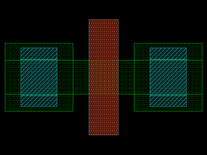
@gf.cell(schematic_function=nmos_schematic, tags=["IHP", "mos", "lv"])
def nmos(
    width: float = 0.15,
    length: float = 0.13,
    nf: int = 1,
    m: int = 1,
    model: str = "sg13_lv_nmos",
) -> Component:
    """Create an NMOS transistor.

    Args:
        width: Total width of the transistor in micrometers.
        length: Gate length in micrometers.
        nf: Number of fingers.
        m: Multiplier (number of parallel devices).
        model: Device model name.

    Returns:
        Component with NMOS transistor layout.

    Raises:
        ValueError: If width, length, or nf is outside allowed range.
    """
    if length < TECH.nmos_min_length or length > TECH.nmos_max_length:
        raise ValueError(
            f"nmos length={length} out of range [{TECH.nmos_min_length}, {TECH.nmos_max_length}]"
        )
    if nf < 1 or nf > TECH.nmos_max_nf:
        raise ValueError(f"nmos nf={nf} out of range [1, {TECH.nmos_max_nf}]")
    if width < TECH.nmos_min_width or width > TECH.nmos_max_width:
        raise ValueError(
            f"nmos width={width} out of range [{TECH.nmos_min_width}, {TECH.nmos_max_width}]"
        )

    c = _mos_core(width, length, nf, is_pmos=False, is_hv=False)
    return c

nmos

import warnings
warnings.filterwarnings("ignore", category=DeprecationWarning)

from ihp import PDK
from ihp import cells

PDK.activate()

c = cells.nmos(width=0.15, length=0.13, nf=1, m=1, model='sg13_lv_nmos').copy()
c.draw_ports()
c.plot()

nmos_hv

Create a high-voltage NMOS transistor.

Parameters:

Name Type Description Default
width float

Total width of the transistor in micrometers.

0.6
length float

Gate length in micrometers.

0.45
nf int

Number of fingers.

1
m int

Multiplier (number of parallel devices).

1
model str

Device model name.

'sg13_hv_nmos'

Returns:

Type Description
Component

Component with HV NMOS transistor layout.

Raises:

Type Description
ValueError

If width, length, or nf is outside allowed range.

Source code in ihp/cells/fet_transistors.py
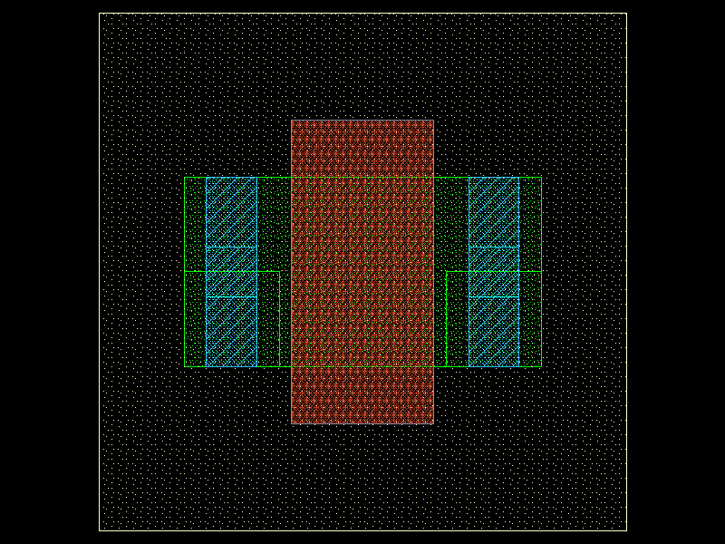
@gf.cell(schematic_function=nmos_hv_schematic, tags=["IHP", "mos", "hv"])
def nmos_hv(
    width: float = 0.60,
    length: float = 0.45,
    nf: int = 1,
    m: int = 1,
    model: str = "sg13_hv_nmos",
) -> Component:
    """Create a high-voltage NMOS transistor.

    Args:
        width: Total width of the transistor in micrometers.
        length: Gate length in micrometers.
        nf: Number of fingers.
        m: Multiplier (number of parallel devices).
        model: Device model name.

    Returns:
        Component with HV NMOS transistor layout.

    Raises:
        ValueError: If width, length, or nf is outside allowed range.
    """
    if width < TECH.nmos_hv_min_width or width > TECH.nmos_hv_max_width:
        raise ValueError(
            f"nmos_hv width={width} out of range [{TECH.nmos_hv_min_width}, {TECH.nmos_hv_max_width}]"
        )
    if length < TECH.nmos_hv_min_length or length > TECH.nmos_hv_max_length:
        raise ValueError(
            f"nmos_hv length={length} out of range [{TECH.nmos_hv_min_length}, {TECH.nmos_hv_max_length}]"
        )
    if nf < 1 or nf > TECH.nmos_hv_max_nf:
        raise ValueError(f"nmos_hv nf={nf} out of range [1, {TECH.nmos_hv_max_nf}]")

    c = _mos_core(width, length, nf, is_pmos=False, is_hv=True)
    return c

nmos_hv

import warnings
warnings.filterwarnings("ignore", category=DeprecationWarning)

from ihp import PDK
from ihp import cells

PDK.activate()

c = cells.nmos_hv(width=0.6, length=0.45, nf=1, m=1, model='sg13_hv_nmos').copy()
c.draw_ports()
c.plot()

npn13G2

Returns the IHP npn13G2 BJT transistor as a gdsfactory Component.

Parameters:

Name Type Description Default
Nx int

Number of emitter fingers in the x-direction.

1
Ny int

Number of emitter fingers in the y-direction.

1
emitter_length float

Length of the emitter region in microns.

0.9
emitter_width float

Width of the emitter region in microns.

0.7
STI float

Shallow Trench Isolation width in microns.

0.44
baspolyx float

Base poly extension in x-direction in microns.

0.3
bipwinx float

Bipolar window extension in x-direction in microns.

0.07
bipwiny float

Bipolar window extension in y-direction in microns.

0.1
empolyx float

Emitter poly extension in x-direction in microns.

0.15
empolyy float

Emitter poly extension in y-direction in microns.

0.18
text str

Text label for the transistor.

'npn13G2'
CMetY1 float

Contact metal Y1 dimension in microns.

0
CMetY2 float

Contact metal Y2 dimension in microns.

0

Returns:

Type Description
Component

gdsfactory.Component: The generated npn13G2 transistor layout.

Raises:

Type Description
ValueError

If finger count is outside allowed range.

Source code in ihp/cells/bjt_transistors.py
 97
 98
 99
100
101
102
103
104
105
106
107
108
109
110
111
112
113
114
115
116
117
118
119
120
121
122
123
124
125
126
127
128
129
130
131
132
133
134
135
136
137
138
139
140
141
142
143
144
145
146
147
148
149
150
151
152
153
154
155
156
157
158
159
160
161
162
163
164
165
166
167
168
169
170
171
172
173
174
175
176
177
178
179
180
181
182
183
184
185
186
187
188
189
190
191
192
193
194
195
196
197
198
199
200
201
202
203
204
205
206
207
208
209
210
211
212
213
214
215
216
217
218
219
220
221
222
223
224
225
226
227
228
229
230
231
232
233
234
235
236
237
238
239
240
241
242
243
244
245
246
247
248
249
250
251
252
253
254
255
256
257
258
259
260
261
262
263
264
265
266
267
268
269
270
271
272
273
274
275
276
277
278
279
280
281
282
283
284
285
286
287
288
289
290
291
292
293
294
295
296
297
298
299
300
301
302
303
304
305
306
307
308
309
310
311
312
313
314
315
316
317
318
319
320
321
322
323
324
325
326
327
328
329
330
331
332
333
334
335
336
337
338
339
340
341
342
343
344
345
346
347
348
349
350
351
352
353
354
355
356
357
358
359
360
361
362
363
364
365
366
367
368
369
370
371
372
373
374
375
376
377
378
379
380
381
382
383
384
385
386
387
388
389
390
391
392
393
394
395
396
397
398
399
400
401
402
403
404
405
406
407
408
409
410
411
412
413
414
415
416
417
418
419
420
421
422
423
424
425
426
427
428
429
430
431
432
433
434
435
436
437
438
439
440
441
442
443
444
445
446
447
448
449
450
451
452
453
454
455
456
457
458
459
460
461
462
463
464
465
466
467
468
469
470
471
472
473
474
475
476
477
478
479
480
481
482
483
484
485
486
487
488
489
490
491
492
493
494
495
496
497
498
499
500
501
502
503
504
505
506
507
508
509
510
511
512
513
514
515
516
517
518
519
520
521
522
523
524
525
526
527
528
529
530
531
532
533
534
535
536
537
538
539
540
541
542
543
544
545
546
547
548
549
550
551
552
553
554
555
556
557
558
559
560
561
562
563
564
565
566
567
568
569
570
571
572
573
574
575
576
577
578
579
580
581
582
583
584
585
586
587
588
589
590
591
592
593
594
595
596
597
598
599
600
601
602
603
604
605
606
607
608
609
610
611
612
613
614
615
616
617
618
619
620
621
622
623
624
625
626
627
628
629
630
631
632
633
634
635
636
637
638
639
640
641
642
643
644
645
646
647
648
649
650
651
652
653
654
655
656
657
658
659
660
661
662
663
664
665
666
667
668
669
670
671
672
673
674
675
676
677
678
679
680
681
682
683
684
685
686
687
688
689
690
691
692
693
694
695
696
697
698
699
700
701
702
703
704
705
706
707
708
709
710
711
712
713
714
715
716
717
718
719
720
721
722
723
724
725
726
727
728
729
730
731
732
733
734
735
736
737
738
739
740
741
742
743
744
745
746
747
748
749
750
751
752
753
754
755
756
757
758
759
760
761
762
763
764
765
766
767
768
769
770
771
772
773
774
775
776
777
778
779
780
781
782
783
784
785
786
787
788
@gf.cell(schematic_function=npn13G2_schematic, tags=["IHP", "bjt", "npn"])
def npn13G2(
    baspolyx: float = 0.3,
    bipwinx: float = 0.07,
    bipwiny: float = 0.1,
    empolyx: float = 0.15,
    empolyy: float = 0.18,
    STI: float = 0.44,
    emitter_length: float = 0.9,
    emitter_width: float = 0.7,
    Nx: int = 1,
    Ny: int = 1,
    text: str = "npn13G2",
    CMetY1: float = 0,
    CMetY2: float = 0,
) -> gf.Component:
    """Returns the IHP npn13G2 BJT transistor as a gdsfactory Component.

    Args:
        Nx: Number of emitter fingers in the x-direction.
        Ny: Number of emitter fingers in the y-direction.
        emitter_length: Length of the emitter region in microns.
        emitter_width: Width of the emitter region in microns.
        STI: Shallow Trench Isolation width in microns.
        baspolyx: Base poly extension in x-direction in microns.
        bipwinx: Bipolar window extension in x-direction in microns.
        bipwiny: Bipolar window extension in y-direction in microns.
        empolyx: Emitter poly extension in x-direction in microns.
        empolyy: Emitter poly extension in y-direction in microns.
        text: Text label for the transistor.
        CMetY1: Contact metal Y1 dimension in microns.
        CMetY2: Contact metal Y2 dimension in microns.

    Returns:
        gdsfactory.Component: The generated npn13G2 transistor layout.

    Raises:
        ValueError: If finger count is outside allowed range.
    """
    total_nx = Nx * Ny
    if total_nx < _TECH.npn_min_nx or total_nx > _TECH.npn_max_nx:
        raise ValueError(
            f"npn13G2 Nx*Ny={total_nx} out of range [{_TECH.npn_min_nx}, {_TECH.npn_max_nx}]"
        )

    c = gf.Component()

    layer_via1: LayerSpec = "Via1drawing"
    layer_metal1: LayerSpec = "Metal1drawing"
    layer_cont: LayerSpec = "Contdrawing"
    layer_emwind: LayerSpec = "EmWinddrawing"
    layer_activmask: LayerSpec = "Activmask"
    layer_activ: LayerSpec = "Activdrawing"
    layer_metal1: LayerSpec = "Metal1drawing"
    layer_metal1_pin: LayerSpec = "Metal1pin"
    layer_metal2_pin: LayerSpec = "Metal2pin"
    layer_metal2: LayerSpec = "Metal2drawing"
    layer_nSDblock: LayerSpec = "nSDblock"
    layer_text: LayerSpec = "TEXTdrawing"
    layer_trans: LayerSpec = "TRANSdrawing"
    layer_pSD: LayerSpec = "pSDdrawing"

    ActivShift = 0.01
    ActivShift = 0.0

    # for multiplied npn: le has to be bigger
    stepX = 1.85
    stretchX = stepX * (Nx - 1)

    # stretchX = stepX * (Nx - 1)
    bipwinyoffset = (2 * (bipwiny - 0.1) - 0) / 2
    empolyyoffset = (2 * (empolyy - 0.18)) / 2

    empolyxoffset = (2 * (empolyx - 0.15)) / 2
    baspolyxoffset = (2 * (baspolyx - 0.3)) / 2
    STIoffset = (2 * (STI - 0.44)) / 2

    tmp = emitter_length
    le = emitter_width
    we = tmp

    nSDBlockShift = (
        0.43 - le
    )  # 23.07.09: needed to draw nSDBlock shorter in small pCell

    leoffset = 0  # ((le - 0.07) / 2)

    ##############
    # npn13G2_base

    pcStepY = 0.41
    yOffset = 0.20

    pcRepeatY = 4

    if Nx > 1:
        CMetY1 = 1.01 + we / 2 + leoffset + bipwinyoffset + empolyyoffset
        CMetY2 = 0.57 + we / 2 + leoffset + bipwinyoffset + empolyyoffset
    else:
        CMetY1 = 0.8 + we / 2 + leoffset + bipwinyoffset + empolyyoffset
        CMetY2 = 0.56 + we / 2 + leoffset + bipwinyoffset + empolyyoffset

    for pcIndexX in range(int(math.floor(Nx))):
        # loop for generate the given number of vias in variable pcRepeatY
        # two vias are generated per loop
        for pcIndexY in range(int(math.floor(pcRepeatY))):
            # Via on left side
            via1_size = 0.19
            left = (stepX * pcIndexX) - 0.3
            bottom = (
                -(
                    (-0.3 - yOffset - leoffset - bipwinyoffset - empolyyoffset)
                    + (pcIndexY * pcStepY)
                )
                + 0.2
                - via1_size
            )
            c.add_ref(
                gf.components.rectangle(
                    size=(
                        via1_size,
                        via1_size,
                    ),
                    layer=layer_via1,
                )
            ).move((left, bottom))

            left = (stepX * pcIndexX) + 0.11
            # Via on the right side
            c.add_ref(
                gf.components.rectangle(
                    size=(
                        via1_size,
                        via1_size,
                    ),
                    layer=layer_via1,
                )
            ).move((left, bottom))

        # Emitter metal
        left = (stepX * pcIndexX) - 0.35
        bottom = -(0.335 + we / 2 + leoffset + bipwinyoffset + empolyyoffset)
        right = stepX * pcIndexX + 0.35
        top = -(-0.32 - we / 2 - leoffset - bipwinyoffset - empolyyoffset)
        c.add_ref(
            gf.components.rectangle(
                size=(
                    right - left,
                    top - bottom,
                ),
                layer=layer_metal1,
            )
        ).move((left, bottom))
        # Cont layer
        left = stepX * pcIndexX - 0.79 - le / 2
        top = -(-0.76 - we / 2 - leoffset - bipwinyoffset - empolyyoffset)
        right = stepX * pcIndexX + 0.79 + le / 2
        bottom = -(-0.6 - we / 2 - leoffset - bipwinyoffset - empolyyoffset)
        c.add_ref(
            gf.components.rectangle(
                size=(
                    right - left,
                    top - bottom,
                ),
                layer=layer_cont,
            )
        ).move((left, bottom))

        left = stepX * pcIndexX - 0.76
        top = -(0.61 + we / 2 - leoffset - bipwinyoffset - empolyyoffset)
        right = stepX * pcIndexX + 0.76
        bottom = -(0.77 + we / 2 - leoffset - bipwinyoffset - empolyyoffset)
        c.add_ref(
            gf.components.rectangle(
                size=(
                    right - left,
                    top - bottom,
                ),
                layer=layer_cont,
            )
        ).move((left, bottom))

        # EmWind
        left = stepX * pcIndexX - le / 2
        top = we / 2 + leoffset
        right = stepX * pcIndexX + le / 2
        bottom = -we / 2 - leoffset
        c.add_ref(
            gf.components.rectangle(
                size=(
                    right - left,
                    top - bottom,
                ),
                layer=layer_emwind,
            )
        ).move((left, bottom))

        # Activmask
        xl = stepX * pcIndexX - 0.06
        xh = xl + 0.12
        yl = -0.24 - leoffset
        yh = -yl

        c.add_polygon(
            [
                (xh + 0.865, -yl + 0.74),
                (xl - 0.865, -yl + 0.74),
                (xl - 0.865, -yh - 0.38),
                (xl - 0.385, -yh - 0.38),
                (xl - 0.175, -yh - 0.59),
                (xh + 0.175, -yh - 0.59),
                (xh + 0.385, -yh - 0.38),
                (xh + 0.865, -yh - 0.38),
            ],
            layer=layer_activmask,
        )

        # Activ
        left = (
            stepX * pcIndexX
            - 0.89
            - le / 2
            - empolyxoffset
            - baspolyxoffset
            - STIoffset
        )
        top = -(-0.83 - we / 2 - leoffset - bipwinyoffset - empolyyoffset)
        right = (
            stepX * pcIndexX
            + 0.89
            + le / 2
            + empolyxoffset
            + baspolyxoffset
            + STIoffset
        )
        bottom = -(-0.89 - we / 2 + 0.36 - leoffset - bipwinyoffset - empolyyoffset)
        c.add_ref(
            gf.components.rectangle(
                size=(
                    right - left,
                    top - bottom,
                ),
                layer=layer_activ,
            )
        ).move((left, bottom))

        c.add_polygon(
            [
                (
                    stepX * pcIndexX
                    + 0.94
                    + le / 2
                    + empolyxoffset
                    + baspolyxoffset
                    + STIoffset,
                    -(1.98 + we / 2 + leoffset + bipwinyoffset + empolyyoffset),
                ),
                (
                    stepX * pcIndexX
                    + 0.94
                    + le / 2
                    + empolyxoffset
                    + baspolyxoffset
                    + STIoffset,
                    -(0.45 + we / 2 + leoffset + bipwinyoffset + empolyyoffset),
                ),
                (
                    stepX * pcIndexX
                    + 0.52
                    + le / 2
                    + empolyxoffset
                    + baspolyxoffset
                    + STIoffset,
                    -(0.03 + we / 2 + leoffset + bipwinyoffset + empolyyoffset),
                ),
                (
                    stepX * pcIndexX
                    + 0.52
                    + le / 2
                    + empolyxoffset
                    + baspolyxoffset
                    + STIoffset,
                    -(
                        -0.6
                        - we / 2
                        + leoffset
                        + bipwinyoffset
                        + empolyyoffset
                        + nSDBlockShift
                    ),
                ),
                (
                    stepX * pcIndexX
                    + 0.27
                    + le / 2
                    + empolyxoffset
                    + baspolyxoffset
                    + STIoffset,
                    -(
                        -0.85
                        - we / 2
                        + leoffset
                        + bipwinyoffset
                        + empolyyoffset
                        + nSDBlockShift
                    ),
                ),
                (
                    stepX * pcIndexX
                    - 0.27
                    - le / 2
                    - empolyxoffset
                    - baspolyxoffset
                    - STIoffset,
                    -(
                        -0.85
                        - we / 2
                        + leoffset
                        + bipwinyoffset
                        + empolyyoffset
                        + nSDBlockShift
                    ),
                ),
                (
                    stepX * pcIndexX
                    - 0.52
                    - le / 2
                    - empolyxoffset
                    - baspolyxoffset
                    - STIoffset,
                    -(
                        -0.6
                        - we / 2
                        + leoffset
                        + bipwinyoffset
                        + empolyyoffset
                        + nSDBlockShift
                    ),
                ),
                (
                    stepX * pcIndexX
                    - 0.52
                    - le / 2
                    - empolyxoffset
                    - baspolyxoffset
                    - STIoffset,
                    -(0.03 + we / 2 + leoffset + bipwinyoffset + empolyyoffset),
                ),
                (
                    stepX * pcIndexX
                    - 0.94
                    - le / 2
                    - empolyxoffset
                    - baspolyxoffset
                    - STIoffset,
                    -(0.45 + we / 2 + leoffset + bipwinyoffset + empolyyoffset),
                ),
                (
                    stepX * pcIndexX
                    - 0.94
                    - le / 2
                    - empolyxoffset
                    - baspolyxoffset
                    - STIoffset,
                    -(1.98 + we / 2 + leoffset + bipwinyoffset + empolyyoffset),
                ),
            ],
            layer=layer_nSDblock,
        )

        # Collector metal
        left = -0.89 - le / 2
        top = CMetY1
        right = stretchX + 0.89 + le / 2
        bottom = CMetY2
        c.add_ref(
            gf.components.rectangle(
                size=(
                    right - left,
                    top - bottom,
                ),
                layer=layer_metal1,
            )
        ).move((left, bottom))

        # Base metal
        left = -0.94 - le / 2
        bottom = -(0.81 + we / 2 + leoffset + bipwinyoffset + empolyyoffset)
        right = stretchX + 0.94 + le / 2
        top = -(0.57 + we / 2 + leoffset + bipwinyoffset + empolyyoffset)
        c.add_ref(
            gf.components.rectangle(
                size=(
                    right - left,
                    top - bottom,
                ),
                layer=layer_metal1,
            )
        ).move((left, bottom))

        # Metal2
        left = -0.89 - le / 2
        bottom = -(0.335 + we / 2 + leoffset + bipwinyoffset + empolyyoffset)
        right = stretchX + 0.89 + le / 2
        top = -(-0.32 - we / 2 - leoffset - bipwinyoffset - empolyyoffset)
        c.add_ref(
            gf.components.rectangle(
                size=(
                    right - left,
                    top - bottom,
                ),
                layer=layer_metal2,
            )
        ).move((left, bottom))

        c.add_label(
            text=text,
            layer=layer_text,
            position=(
                0.015,
                1.86 + we / 2 + leoffset + bipwinyoffset + empolyyoffset,
            ),
        )

        c.add_polygon(
            [
                (
                    stretchX + 2.45,
                    (2.43 + we / 2 + leoffset + bipwinyoffset + empolyyoffset),
                ),
                (-2.45, (2.43 + we / 2 + leoffset + bipwinyoffset + empolyyoffset)),
                (-2.45, (-1.98 - we / 2 - leoffset - bipwinyoffset - empolyyoffset)),
                (
                    stretchX + 2.45,
                    (-1.98 - we / 2 - leoffset - bipwinyoffset - empolyyoffset),
                ),
            ],
            layer=layer_trans,
        )

        c.add_polygon(
            [
                (
                    stretchX + 3.35,
                    (3.33 + we / 2 + leoffset + bipwinyoffset + empolyyoffset),
                ),
                (
                    stretchX + 2.45,
                    (3.33 + we / 2 + leoffset + bipwinyoffset + empolyyoffset),
                ),
                (
                    stretchX + 2.45,
                    (-1.98 - we / 2 - leoffset - bipwinyoffset - empolyyoffset),
                ),
                (-2.45, (-1.98 - we / 2 - leoffset - bipwinyoffset - empolyyoffset)),
                (-2.45, (2.43 + we / 2 + leoffset + bipwinyoffset + empolyyoffset)),
                (
                    stretchX + 2.45,
                    (2.43 + we / 2 + leoffset + bipwinyoffset + empolyyoffset),
                ),
                (
                    stretchX + 2.45,
                    (3.33 + we / 2 + leoffset + bipwinyoffset + empolyyoffset),
                ),
                (-3.35, (3.33 + we / 2 + leoffset + bipwinyoffset + empolyyoffset)),
                (-3.35, (-2.88 - we / 2 - leoffset - bipwinyoffset - empolyyoffset)),
                (
                    stretchX + 3.35,
                    (-2.88 - we / 2 - leoffset - bipwinyoffset - empolyyoffset),
                ),
            ],
            layer=layer_pSD,
        )

        c.add_polygon(
            [
                (
                    stretchX + 3.15 + ActivShift,
                    3.13
                    + we / 2
                    + leoffset
                    + bipwinyoffset
                    + empolyyoffset
                    + ActivShift,
                ),
                (
                    stretchX + 2.65 + ActivShift,
                    3.13
                    + we / 2
                    + leoffset
                    + bipwinyoffset
                    + empolyyoffset
                    + ActivShift,
                ),
                (
                    stretchX + 2.65 + ActivShift,
                    -2.18
                    - we / 2
                    - leoffset
                    - bipwinyoffset
                    - empolyyoffset
                    - ActivShift,
                ),
                (
                    -2.65 - ActivShift,
                    -2.18
                    - we / 2
                    - leoffset
                    - bipwinyoffset
                    - empolyyoffset
                    - ActivShift,
                ),
                (
                    -2.65 - ActivShift,
                    2.63
                    + we / 2
                    + leoffset
                    + bipwinyoffset
                    + empolyyoffset
                    + ActivShift,
                ),
                (
                    stretchX + 2.65 + ActivShift,
                    2.63
                    + we / 2
                    + leoffset
                    + bipwinyoffset
                    + empolyyoffset
                    + ActivShift,
                ),
                (
                    stretchX + 2.65 + ActivShift,
                    3.13
                    + we / 2
                    + leoffset
                    + bipwinyoffset
                    + empolyyoffset
                    + ActivShift,
                ),
                (
                    -3.15 - ActivShift,
                    3.13
                    + we / 2
                    + leoffset
                    + bipwinyoffset
                    + empolyyoffset
                    + ActivShift,
                ),
                (
                    -3.15 - ActivShift,
                    -2.68
                    - we / 2
                    - leoffset
                    - bipwinyoffset
                    - empolyyoffset
                    - ActivShift,
                ),
                (
                    stretchX + 3.15 + ActivShift,
                    -2.68
                    - we / 2
                    - leoffset
                    - bipwinyoffset
                    - empolyyoffset
                    - ActivShift,
                ),
            ],
            layer=layer_activ,
        )

    if Nx > 1:
        left = -0.89 - le / 2
        bottom = 0.57 + we / 2 - leoffset - bipwinyoffset - empolyyoffset
        right = stretchX + 0.89 + le / 2
        top = 1.01 + we / 2 - leoffset - bipwinyoffset - empolyyoffset
        c.add_ref(
            gf.components.rectangle(
                size=(
                    right - left,
                    top - bottom,
                ),
                layer=layer_metal1_pin,
            )
        ).move((left, bottom))
        c.add_label(
            text="C",
            layer=layer_text,
            position=(
                0.5 * (left + right),
                0.5 * (top + bottom),
            ),
        )
    else:
        left = -0.89 - le / 2
        bottom = 0.56 + we / 2 + leoffset + bipwinyoffset + empolyyoffset
        right = stretchX + 0.89 + le / 2
        top = 0.8 + we / 2 + leoffset + bipwinyoffset + empolyyoffset
        c.add_ref(
            gf.components.rectangle(
                size=(
                    right - left,
                    top - bottom,
                ),
                layer=layer_metal1_pin,
            )
        ).move((left, bottom))
        c.add_label(
            text="C",
            layer=layer_text,
            position=(
                0.5 * (left + right),
                0.5 * (top + bottom),
            ),
        )
    # Collector port
    c.add_port(
        "C",
        center=(0.5 * (left + right), 0.5 * (top + bottom)),
        width=_snap_width_to_grid(top - bottom),
        layer=layer_metal1_pin,
        orientation=180.0,
        port_type="electrical",
    )

    left = -0.94 - le / 2
    bottom = -0.81 - we / 2 - leoffset - bipwinyoffset - empolyyoffset
    right = stretchX + 0.94 + le / 2
    top = -0.57 - we / 2 - leoffset - bipwinyoffset - empolyyoffset
    c.add_ref(
        gf.components.rectangle(
            size=(
                right - left,
                top - bottom,
            ),
            layer=layer_metal1_pin,
        )
    ).move((left, bottom))
    c.add_label(
        text="B",
        layer=layer_text,
        position=(
            0.5 * (left + right),
            0.5 * (top + bottom),
        ),
    )

    # Base port
    c.add_port(
        "B",
        center=(0.5 * (left + right), 0.5 * (top + bottom)),
        width=_snap_width_to_grid(top - bottom),
        layer=layer_metal1_pin,
        orientation=180.0,
        port_type="electrical",
    )

    left = -0.71 - le / 2
    bottom = -0.335 - we / 2 - leoffset - bipwinyoffset - empolyyoffset
    right = stretchX + 0.71 + le / 2
    top = 0.32 + we / 2 + leoffset + bipwinyoffset + empolyyoffset
    c.add_ref(
        gf.components.rectangle(
            size=(
                right - left,
                top - bottom,
            ),
            layer=layer_metal2_pin,
        )
    ).move((left, bottom))
    c.add_label(
        text="E",
        layer=layer_text,
        position=(
            0.5 * (left + right),
            0.5 * (top + bottom),
        ),
    )

    pcLabelText = f"Ae={int(Nx):d}*{int(Ny):d}*{le:.2f}*{we:.2f}"
    c.add_label(text=pcLabelText, layer=layer_text, position=(-1.977, -2.546))

    # Emitter port
    c.add_port(
        "E",
        center=(0.5 * (left + right), 0.5 * (top + bottom)),
        width=_snap_width_to_grid(top - bottom),
        layer=layer_metal2_pin,
        orientation=180.0,
        port_type="electrical",
    )

    return c

npn13G2

import warnings
warnings.filterwarnings("ignore", category=DeprecationWarning)

from ihp import PDK
from ihp import cells

PDK.activate()

c = cells.npn13G2(baspolyx=0.3, bipwinx=0.07, bipwiny=0.1, empolyx=0.15, empolyy=0.18, STI=0.44, emitter_length=0.9, emitter_width=0.7, Nx=1, Ny=1, text='npn13G2', CMetY1=0, CMetY2=0).copy()
c.draw_ports()
c.plot()

npn13G2L

Builds the IHP npn13G2L BJT transistor as a gdsfactory Component.

The transistor geometry is defined by the number of emitter fingers and the dimensions of each emitter finger.

Parameters:

Name Type Description Default
emitter_length float

Length of each emitter finger, in microns.

1
emitter_width float

Width of each emitter finger, in microns.

0.07
Nx int

Number of emitter fingers.

1

Returns:

Type Description
Component

gdsfactory.Component: The generated npn13G2L transistor layout.

Raises:

Type Description
ValueError

If finger count is outside allowed range.

Source code in ihp/cells/bjt_transistors.py
 839
 840
 841
 842
 843
 844
 845
 846
 847
 848
 849
 850
 851
 852
 853
 854
 855
 856
 857
 858
 859
 860
 861
 862
 863
 864
 865
 866
 867
 868
 869
 870
 871
 872
 873
 874
 875
 876
 877
 878
 879
 880
 881
 882
 883
 884
 885
 886
 887
 888
 889
 890
 891
 892
 893
 894
 895
 896
 897
 898
 899
 900
 901
 902
 903
 904
 905
 906
 907
 908
 909
 910
 911
 912
 913
 914
 915
 916
 917
 918
 919
 920
 921
 922
 923
 924
 925
 926
 927
 928
 929
 930
 931
 932
 933
 934
 935
 936
 937
 938
 939
 940
 941
 942
 943
 944
 945
 946
 947
 948
 949
 950
 951
 952
 953
 954
 955
 956
 957
 958
 959
 960
 961
 962
 963
 964
 965
 966
 967
 968
 969
 970
 971
 972
 973
 974
 975
 976
 977
 978
 979
 980
 981
 982
 983
 984
 985
 986
 987
 988
 989
 990
 991
 992
 993
 994
 995
 996
 997
 998
 999
1000
1001
1002
1003
1004
1005
1006
1007
1008
1009
1010
1011
1012
1013
1014
1015
1016
1017
1018
1019
1020
1021
1022
1023
1024
1025
1026
1027
1028
1029
1030
1031
1032
1033
1034
1035
1036
1037
1038
1039
1040
1041
1042
1043
1044
1045
1046
1047
1048
1049
1050
1051
1052
1053
1054
1055
1056
1057
1058
1059
1060
1061
1062
1063
1064
1065
1066
1067
1068
1069
1070
1071
1072
1073
1074
1075
1076
1077
1078
1079
1080
1081
1082
1083
1084
1085
1086
1087
1088
1089
1090
1091
1092
1093
1094
1095
1096
1097
1098
1099
1100
1101
1102
1103
1104
1105
1106
1107
1108
1109
1110
1111
1112
1113
1114
1115
1116
1117
1118
1119
1120
1121
1122
1123
1124
1125
1126
1127
1128
1129
1130
1131
1132
1133
1134
1135
1136
1137
1138
1139
1140
1141
1142
1143
1144
1145
1146
1147
1148
1149
1150
1151
1152
1153
1154
1155
1156
1157
1158
1159
1160
1161
1162
1163
1164
1165
1166
1167
1168
1169
1170
1171
1172
1173
1174
1175
1176
1177
1178
1179
1180
1181
1182
1183
1184
1185
1186
1187
1188
1189
1190
1191
1192
1193
1194
1195
1196
1197
1198
1199
1200
1201
1202
1203
1204
1205
1206
1207
1208
1209
1210
1211
1212
1213
1214
1215
1216
1217
1218
1219
1220
1221
1222
1223
1224
1225
1226
1227
1228
1229
1230
1231
1232
1233
1234
1235
1236
1237
1238
1239
1240
1241
1242
1243
1244
1245
1246
1247
1248
1249
1250
1251
1252
1253
1254
1255
1256
1257
1258
1259
1260
1261
1262
1263
1264
1265
1266
1267
1268
1269
1270
1271
1272
1273
1274
1275
1276
1277
1278
1279
1280
1281
1282
1283
1284
1285
1286
1287
1288
1289
1290
1291
1292
1293
1294
1295
1296
1297
1298
1299
1300
1301
1302
1303
1304
1305
1306
1307
1308
1309
1310
1311
1312
1313
1314
1315
1316
1317
1318
1319
1320
1321
1322
1323
1324
1325
1326
1327
1328
1329
1330
1331
1332
1333
1334
1335
1336
1337
1338
1339
1340
1341
1342
1343
1344
1345
1346
1347
1348
1349
1350
1351
1352
1353
1354
1355
1356
1357
1358
1359
1360
1361
1362
1363
1364
1365
1366
1367
1368
1369
1370
1371
1372
1373
1374
1375
1376
1377
1378
1379
1380
1381
1382
1383
1384
1385
1386
1387
1388
1389
1390
1391
1392
1393
1394
@gf.cell(schematic_function=npn13G2L_schematic, tags=["IHP", "bjt", "npn"])
def npn13G2L(
    emitter_length: float = 1,
    emitter_width: float = 0.07,
    Nx: int = 1,
) -> gf.Component:
    """Builds the IHP npn13G2L BJT transistor as a gdsfactory Component.

    The transistor geometry is defined by the number of emitter fingers and the dimensions
    of each emitter finger.

    Args:
        emitter_length: Length of each emitter finger, in microns.
        emitter_width: Width of each emitter finger, in microns.
        Nx: Number of emitter fingers.

    Returns:
        gdsfactory.Component: The generated npn13G2L transistor layout.

    Raises:
        ValueError: If finger count is outside allowed range.
    """
    if Nx < _TECH.npn_min_nx or Nx > _TECH.npn_max_nx:
        raise ValueError(
            f"npn13G2L Nx={Nx} out of range [{_TECH.npn_min_nx}, {_TECH.npn_max_nx}]"
        )

    c = gf.Component()

    layer_EmWind: LayerSpec = "EmWinddrawing"
    layer_HeatTrans: LayerSpec = "HeatTransdrawing"
    layer_activ: LayerSpec = "Activdrawing"
    layer_activ_mask: LayerSpec = "Activmask"
    layer_via1: LayerSpec = "Via1drawing"
    layer_cont: LayerSpec = "Contdrawing"
    layer_metal1: LayerSpec = "Metal1drawing"
    layer_metal1_pin: LayerSpec = "Metal1pin"
    layer_metal2: LayerSpec = "Metal2drawing"
    layer_metal2_pin: LayerSpec = "Metal2pin"
    layer_trans: LayerSpec = "TRANSdrawing"
    layer_text: LayerSpec = "TEXTdrawing"
    layer_pSD: LayerSpec = "pSDdrawing"

    le = emitter_length
    we = emitter_width
    # masterLib = "SG13_dev"

    # emPoly_enc_vert = 0.16
    # emPoly_enc_hori = 0.13
    emWindOrigin_x = 3.865
    emWindOrigin_y = 3.1
    # BiWind_enc_vert = 0.1
    # BiWind_enc_hori = 0.07
    # ColWind_enc_vert = 0.58
    # ColWind_enc_hori = 1.515
    Activ_enc_vert = 0.28
    Activ_enc_hori = 1.365
    # BasPoly_enc_vert = 0.45
    # BasPoly_enc_hori = 0.58
    Col_Metal1_distance = 0.975
    Col_Metal1_width = 0.39
    Bas_Metal1_distance = 0.32
    Bas_Metal1_width = 0.16
    Emi_Metal1_enc_vert = 0.2
    Emi_Metal1_enc_hori = 0.095

    column_pitch = 2.8

    c.add_ref(
        gf.components.rectangle(
            size=(we, le),
            layer=layer_EmWind,
        ),
        columns=Nx,
        column_pitch=column_pitch,
    ).move((emWindOrigin_x, emWindOrigin_y))

    c.add_ref(
        gf.components.rectangle(
            size=(
                we + 0.1,
                le + 0.1,
            ),
            layer=layer_HeatTrans,
        ),
        columns=Nx,
        column_pitch=column_pitch,
    ).move((emWindOrigin_x - 0.05, emWindOrigin_y - 0.05))

    c.add_label(
        text="npn13G2L",
        layer=layer_HeatTrans,
        position=(
            0.5 * (2 * emWindOrigin_x + we),
            0.5 * (2 * emWindOrigin_y + le),
        ),
    )

    # Activ Drawing
    outer = c << gf.components.rectangle(
        size=(
            we + 2 * Activ_enc_hori,
            le + 2 * Activ_enc_vert,
        ),
        layer=layer_activ,
    )
    outer.move((emWindOrigin_x - Activ_enc_hori, emWindOrigin_y - Activ_enc_vert))

    # Activ mask
    inner = c << gf.components.rectangle(
        size=(
            0.705 - Emi_Metal1_enc_hori,
            le + 2 * Activ_enc_vert,
        ),
        layer=layer_activ_mask,
    )
    inner.move((emWindOrigin_x - 0.705, emWindOrigin_y - Activ_enc_vert))

    inner1 = c << gf.components.rectangle(
        size=(
            0.705 - Emi_Metal1_enc_hori,
            le + 2 * Activ_enc_vert,
        ),
        layer=layer_activ_mask,
    )
    inner1.move(
        (emWindOrigin_x + we + Emi_Metal1_enc_hori, emWindOrigin_y - Activ_enc_vert)
    )

    # Combine mask's rectangles in order to remove them from activ
    inners = gf.boolean(inner, inner1, operation="or", layer=layer_activ_mask)

    c.add_ref(inners, columns=Nx, column_pitch=column_pitch)

    c.add_ref(
        gf.boolean(
            outer,
            inners,
            operation="not",
            layer=layer_activ,
            layer1=layer_activ,
            layer2=layer_activ_mask,
        ),
        columns=Nx,
        column_pitch=column_pitch,
    )
    # Delete the rectangle that was covering the whole region
    outer.delete()

    # Draw contacts and Via
    c.add_ref(
        gf.components.rectangle(
            size=(
                0.19,
                0.2 + le,
            ),
            layer=layer_via1,
        ),
        columns=Nx,
        column_pitch=column_pitch,
    ).move((3.805, 3))

    c.add_ref(
        gf.components.rectangle(
            size=(
                0.16,
                0.3 + le,
            ),
            layer=layer_cont,
        ),
        columns=Nx,
        column_pitch=column_pitch,
    ).move((2.68, 2.95))

    c.add_ref(
        gf.components.rectangle(
            size=(
                0.16,
                0.3 + le,
            ),
            layer=layer_cont,
        ),
        columns=Nx,
        column_pitch=column_pitch,
    ).move((3.82, 2.95))

    c.add_ref(
        gf.components.rectangle(
            size=(
                0.16,
                0.3 + le,
            ),
            layer=layer_cont,
        ),
        columns=Nx,
        column_pitch=column_pitch,
    ).move((4.96, 2.95))

    cont_cnt = fix((le + 0.21) / (0.16 + 0.18))

    for i in range(int(cont_cnt + 1)):
        c.add_ref(
            gf.components.rectangle(
                size=(
                    0.16,
                    0.16,
                ),
                layer=layer_cont,
            ),
            columns=Nx,
            column_pitch=column_pitch,
        ).move((3.385, 2.89 + i * (0.16 + 0.18)))

        c.add_ref(
            gf.components.rectangle(
                size=(
                    0.16,
                    0.16,
                ),
                layer=layer_cont,
            ),
            columns=Nx,
            column_pitch=column_pitch,
        ).move((4.255, 2.89 + i * (0.16 + 0.18)))

    # Metals
    # Metal Path upwards
    # Collector
    c.add_ref(
        gf.components.rectangle(
            size=(
                Col_Metal1_width,
                4.1 - 2.82 + le,
            ),
            layer=layer_metal1,
        ),
        columns=Nx,
        column_pitch=column_pitch,
    ).move((emWindOrigin_x - Col_Metal1_distance - Col_Metal1_width, 2.82))

    c.add_ref(
        gf.components.rectangle(
            size=(
                Col_Metal1_width,
                4.1 - 2.82 + le,
            ),
            layer=layer_metal1,
        ),
        columns=Nx,
        column_pitch=column_pitch,
    ).move((emWindOrigin_x + we + Col_Metal1_distance, 2.82))

    c.add_ref(
        gf.components.rectangle(
            size=(
                2 * Col_Metal1_distance + we + 2 * Col_Metal1_width,
                0.65,
            ),
            layer=layer_metal1,
        ),
        columns=Nx,
        column_pitch=column_pitch,
    ).move((emWindOrigin_x - Col_Metal1_distance - Col_Metal1_width, 4.1 + le))

    collector_pin_xmin = emWindOrigin_x - Col_Metal1_distance - Col_Metal1_width
    collector_pin_xmax = (
        collector_pin_xmin + 2 * Col_Metal1_distance + we + 2 * Col_Metal1_width
    )
    # The maximum x depends on the number of elements
    collector_pin_xmax += (Nx - 1) * (collector_pin_xmax - collector_pin_xmin)
    collector_pin_ymin = 4.1 + le
    collector_pin_ymax = collector_pin_ymin + 0.65

    c.add_ref(
        gf.components.rectangle(
            size=(
                2 * Col_Metal1_distance + we + 2 * Col_Metal1_width,
                0.65,
            ),
            layer=layer_metal1_pin,
        ),
        columns=Nx,
        column_pitch=column_pitch,
    ).move((emWindOrigin_x - Col_Metal1_distance - Col_Metal1_width, 4.1 + le))

    c.add_ref(
        gf.components.rectangle(
            size=(
                Bas_Metal1_width,
                1.28 + le,
            ),
            layer=layer_metal1,
        ),
        columns=Nx,
        column_pitch=column_pitch,
    ).move((emWindOrigin_x - Bas_Metal1_distance - Bas_Metal1_width, 2.1))

    c.add_ref(
        gf.components.rectangle(
            size=(
                Bas_Metal1_width,
                1.28 + le,
            ),
            layer=layer_metal1,
        ),
        columns=Nx,
        column_pitch=column_pitch,
    ).move((emWindOrigin_x + we + Bas_Metal1_distance, 2.1))

    c.add_ref(
        gf.components.rectangle(
            size=(
                2 * Bas_Metal1_distance + we + 2 * Bas_Metal1_width,
                0.65,
            ),
            layer=layer_metal1,
        ),
        columns=Nx,
        column_pitch=column_pitch,
    ).move((emWindOrigin_x - Bas_Metal1_distance - Bas_Metal1_width, 1.45))

    base_pin_xmin = emWindOrigin_x - Bas_Metal1_distance - Bas_Metal1_width
    base_pin_xmax = base_pin_xmin + 2 * Bas_Metal1_distance + we + 2 * Bas_Metal1_width
    # The maximum x depends on the number of elements
    base_pin_xmax += (Nx - 1) * column_pitch
    base_pin_ymin = 1.45
    base_pin_ymax = base_pin_ymin + 0.65

    c.add_ref(
        gf.components.rectangle(
            size=(
                2 * Bas_Metal1_distance + we + 2 * Bas_Metal1_width,
                0.65,
            ),
            layer=layer_metal1_pin,
        ),
        columns=Nx,
        column_pitch=column_pitch,
    ).move((emWindOrigin_x - Bas_Metal1_distance - Bas_Metal1_width, 1.45))

    # Emitter
    c.add_ref(
        gf.components.rectangle(
            size=(
                we + 2 * Emi_Metal1_enc_hori,
                le + 2 * Emi_Metal1_enc_vert,
            ),
            layer=layer_metal1,
        ),
        columns=Nx,
        column_pitch=column_pitch,
    ).move((emWindOrigin_x - Emi_Metal1_enc_hori, emWindOrigin_y - Emi_Metal1_enc_vert))

    c.add_ref(
        gf.components.rectangle(
            size=(
                we + 2 * Col_Metal1_distance + 2 * Col_Metal1_width,
                le + 0.4,
            ),
            layer=layer_metal2,
        ),
        columns=Nx,
        column_pitch=column_pitch,
    ).move((emWindOrigin_x - Col_Metal1_distance - Col_Metal1_width, 2.9))

    emitter_pin_xmin = emWindOrigin_x - Col_Metal1_distance - Col_Metal1_width
    emitter_pin_xmax = (
        emitter_pin_xmin + 2 * Col_Metal1_distance + we + 2 * Col_Metal1_width
    )
    # The maximum x depends on the number of elements
    emitter_pin_xmax += (Nx - 1) * (emitter_pin_xmax - emitter_pin_xmin)
    emitter_pin_ymin = 2.9
    emitter_pin_ymax = emitter_pin_ymin + le + 0.4

    c.add_ref(
        gf.components.rectangle(
            size=(
                we + 2 * Col_Metal1_distance + 2 * Col_Metal1_width,
                le + 0.4,
            ),
            layer=layer_metal2_pin,
        ),
        columns=Nx,
        column_pitch=column_pitch,
    ).move((emWindOrigin_x - Col_Metal1_distance - Col_Metal1_width, 2.9))

    # Draw Guard Ring
    c.add_ref(
        gf.components.rectangle(
            size=(
                6 + ((Nx - 1) * 2.8),
                le + 4.4,
            ),
            layer=layer_trans,
        )
    ).move((0.9, 0.9))

    outer = c << gf.components.rectangle(
        size=(
            7.8 + ((Nx - 1) * 2.8),
            le + 6.2,
        ),
        layer=layer_pSD,
    )

    inner = c << gf.components.rectangle(
        size=(
            6 + ((Nx - 1) * 2.8),
            le + 4.4,
        ),
        layer=layer_pSD,
    )
    inner.move((0.9, 0.9))

    c.add_ref(
        gf.boolean(
            outer,
            inner,
            operation="not",
            layer=layer_pSD,
            layer1=layer_pSD,
            layer2=layer_pSD,
        )
    )
    # Delete the rectangle that was covering the whole region
    outer.delete()
    # Delete the inner rectangle used for boolean
    inner.delete()

    outer = c << gf.components.rectangle(
        size=(
            7.4 + ((Nx - 1) * 2.8),
            le + 5.8,
        ),
        layer=layer_activ,
    )
    outer.move((0.2, 0.2))
    inner = c << gf.components.rectangle(
        size=(
            6.4 + ((Nx - 1) * 2.8),
            le + 4.8,
        ),
        layer=layer_activ,
    )
    inner.move((0.7, 0.7))
    c.add_ref(
        gf.boolean(
            outer,
            inner,
            operation="not",
            layer=layer_activ,
            layer1=layer_activ,
            layer2=layer_activ,
        )
    )
    # Delete the rectangle that was covering the whole region
    outer.delete()
    # Delete the inner rectangle used for boolean
    inner.delete()

    # Texts
    pcLabelText = f"Ae={int(Nx):d}*{1:d}*{le:.2f}*{we:.2f}"
    c.add_label(text=pcLabelText, layer=layer_text, position=(1.5, 1.0))

    c.add_label(text="npn13G2L", layer=layer_text, position=(1.75, 1.0))

    if Nx > 1:
        c.add_ref(
            gf.components.rectangle(
                size=(
                    1.77,
                    0.65,
                ),
                layer=layer_metal1,
            ),
            columns=Nx - 1,
            column_pitch=column_pitch,
        ).move((4.415, 1.45))
        c.add_ref(
            gf.components.rectangle(
                size=(
                    1.77,
                    0.65,
                ),
                layer=layer_metal1_pin,
            ),
            columns=Nx - 1,
            column_pitch=column_pitch,
        ).move((4.415, 1.45))

    # Ports
    # Collector port
    c.add_port(
        "C",
        center=(
            0.5 * (collector_pin_xmin + collector_pin_xmax),
            0.5 * (collector_pin_ymin + collector_pin_ymax),
        ),
        width=_snap_width_to_grid(collector_pin_ymax - collector_pin_ymin),
        layer=layer_metal1_pin,
        orientation=180.0,
        port_type="electrical",
    )

    c.add_label(
        text="C",
        layer=layer_text,
        position=(
            0.5 * (collector_pin_xmin + collector_pin_xmax),
            0.5 * (collector_pin_ymin + collector_pin_ymax),
        ),
    )

    # Base port
    c.add_port(
        "B",
        center=(
            0.5 * (base_pin_xmin + base_pin_xmax),
            0.5 * (base_pin_ymin + base_pin_ymax),
        ),
        width=_snap_width_to_grid(base_pin_ymax - base_pin_ymin),
        layer=layer_metal1_pin,
        orientation=180.0,
        port_type="electrical",
    )
    c.add_label(
        text="B",
        layer=layer_text,
        position=(
            0.5 * (base_pin_xmin + base_pin_xmax),
            0.5 * (base_pin_ymin + base_pin_ymax),
        ),
    )

    # Emitter port
    c.add_port(
        "E",
        center=(
            0.5 * (emitter_pin_xmin + emitter_pin_xmax),
            0.5 * (emitter_pin_ymin + emitter_pin_ymax),
        ),
        width=_snap_width_to_grid(emitter_pin_ymax - emitter_pin_ymin),
        layer=layer_metal2_pin,
        orientation=180.0,
        port_type="electrical",
    )
    c.add_label(
        text="E",
        layer=layer_text,
        position=(
            0.5 * (emitter_pin_xmin + emitter_pin_xmax),
            0.5 * (emitter_pin_ymin + emitter_pin_ymax),
        ),
    )

    return c

npn13G2L

import warnings
warnings.filterwarnings("ignore", category=DeprecationWarning)

from ihp import PDK
from ihp import cells

PDK.activate()

c = cells.npn13G2L(emitter_length=1, emitter_width=0.07, Nx=1).copy()
c.draw_ports()
c.plot()

npn13G2V

Builds the IHP npn13G2V BJT transistor as a gdsfactory Component.

The transistor geometry is defined by the number of emitter fingers and the dimensions of each emitter finger.

Parameters:

Name Type Description Default
emitter_length float

Length of each emitter finger, in microns.

1
emitter_width float

Width of each emitter finger, in microns.

0.12
Nx int

Number of emitter fingers.

1

Returns:

Type Description
Component

gdsfactory.Component: The generated npn13G2V transistor layout.

Raises:

Type Description
ValueError

If finger count is outside allowed range.

Source code in ihp/cells/bjt_transistors.py
1445
1446
1447
1448
1449
1450
1451
1452
1453
1454
1455
1456
1457
1458
1459
1460
1461
1462
1463
1464
1465
1466
1467
1468
1469
1470
1471
1472
1473
1474
1475
1476
1477
1478
1479
1480
1481
1482
1483
1484
1485
1486
1487
1488
1489
1490
1491
1492
1493
1494
1495
1496
1497
1498
1499
1500
1501
1502
1503
1504
1505
1506
1507
1508
1509
1510
1511
1512
1513
1514
1515
1516
1517
1518
1519
1520
1521
1522
1523
1524
1525
1526
1527
1528
1529
1530
1531
1532
1533
1534
1535
1536
1537
1538
1539
1540
1541
1542
1543
1544
1545
1546
1547
1548
1549
1550
1551
1552
1553
1554
1555
1556
1557
1558
1559
1560
1561
1562
1563
1564
1565
1566
1567
1568
1569
1570
1571
1572
1573
1574
1575
1576
1577
1578
1579
1580
1581
1582
1583
1584
1585
1586
1587
1588
1589
1590
1591
1592
1593
1594
1595
1596
1597
1598
1599
1600
1601
1602
1603
1604
1605
1606
1607
1608
1609
1610
1611
1612
1613
1614
1615
1616
1617
1618
1619
1620
1621
1622
1623
1624
1625
1626
1627
1628
1629
1630
1631
1632
1633
1634
1635
1636
1637
1638
1639
1640
1641
1642
1643
1644
1645
1646
1647
1648
1649
1650
1651
1652
1653
1654
1655
1656
1657
1658
1659
1660
1661
1662
1663
1664
1665
1666
1667
1668
1669
1670
1671
1672
1673
1674
1675
1676
1677
1678
1679
1680
1681
1682
1683
1684
1685
1686
1687
1688
1689
1690
1691
1692
1693
1694
1695
1696
1697
1698
1699
1700
1701
1702
1703
1704
1705
1706
1707
1708
1709
1710
1711
1712
1713
1714
1715
1716
1717
1718
1719
1720
1721
1722
1723
1724
1725
1726
1727
1728
1729
1730
1731
1732
1733
1734
1735
1736
1737
1738
1739
1740
1741
1742
1743
1744
1745
1746
1747
1748
1749
1750
1751
1752
1753
1754
1755
1756
1757
1758
1759
1760
1761
1762
1763
1764
1765
1766
1767
1768
1769
1770
1771
1772
1773
1774
1775
1776
1777
1778
1779
1780
1781
1782
1783
1784
1785
1786
1787
1788
1789
1790
1791
1792
1793
1794
1795
1796
1797
1798
1799
1800
1801
1802
1803
1804
1805
1806
1807
1808
1809
1810
1811
1812
1813
1814
1815
1816
1817
1818
1819
1820
1821
1822
1823
1824
1825
1826
1827
1828
1829
1830
1831
1832
1833
1834
1835
1836
1837
1838
1839
1840
1841
1842
1843
1844
1845
1846
1847
1848
1849
1850
1851
1852
1853
1854
1855
1856
1857
1858
1859
1860
1861
1862
1863
1864
1865
1866
1867
1868
1869
1870
1871
1872
1873
1874
1875
1876
1877
1878
1879
1880
1881
1882
1883
1884
1885
1886
1887
1888
1889
1890
1891
1892
1893
1894
1895
1896
1897
1898
1899
1900
1901
1902
1903
1904
1905
1906
1907
1908
1909
1910
1911
1912
1913
1914
1915
1916
1917
1918
1919
1920
1921
1922
1923
1924
1925
1926
1927
1928
1929
1930
1931
1932
1933
1934
1935
1936
1937
1938
1939
1940
1941
1942
1943
1944
1945
1946
1947
1948
1949
1950
1951
1952
1953
1954
1955
1956
1957
1958
1959
1960
1961
1962
1963
1964
1965
1966
1967
1968
1969
1970
1971
1972
1973
1974
1975
1976
1977
1978
1979
1980
1981
1982
1983
1984
1985
1986
1987
1988
1989
1990
1991
1992
1993
1994
1995
1996
1997
1998
1999
2000
2001
2002
2003
2004
2005
2006
2007
2008
2009
2010
2011
2012
2013
2014
2015
2016
2017
2018
2019
2020
2021
@gf.cell(schematic_function=npn13G2V_schematic, tags=["IHP", "bjt", "npn"])
def npn13G2V(
    emitter_length: float = 1,
    emitter_width: float = 0.12,
    Nx: int = 1,
) -> gf.Component:
    """Builds the IHP npn13G2V BJT transistor as a gdsfactory Component.

    The transistor geometry is defined by the number of emitter fingers and the dimensions
    of each emitter finger.

    Args:
        emitter_length: Length of each emitter finger, in microns.
        emitter_width: Width of each emitter finger, in microns.
        Nx: Number of emitter fingers.

    Returns:
        gdsfactory.Component: The generated npn13G2V transistor layout.

    Raises:
        ValueError: If finger count is outside allowed range.
    """
    if Nx < _TECH.npn_min_nx or Nx > _TECH.npn_max_nx:
        raise ValueError(
            f"npn13G2V Nx={Nx} out of range [{_TECH.npn_min_nx}, {_TECH.npn_max_nx}]"
        )

    c = gf.Component()

    layer_EmWiHV: LayerSpec = "EmWiHVdrawing"
    layer_HeatTrans: LayerSpec = "HeatTransdrawing"
    layer_activ: LayerSpec = "Activdrawing"
    layer_activ_mask: LayerSpec = "Activmask"
    layer_via1: LayerSpec = "Via1drawing"
    layer_cont: LayerSpec = "Contdrawing"
    layer_metal1: LayerSpec = "Metal1drawing"
    layer_metal1_pin: LayerSpec = "Metal1pin"
    layer_metal2: LayerSpec = "Metal2drawing"
    layer_metal2_pin: LayerSpec = "Metal2pin"
    layer_trans: LayerSpec = "TRANSdrawing"
    layer_text: LayerSpec = "TEXTdrawing"
    layer_pSD: LayerSpec = "pSDdrawing"

    le = emitter_length
    we = emitter_width
    # masterLib = "SG13_dev"

    emWindOrigin_x = 3.81
    emWindOrigin_y = 3.1
    Activ_enc_vert = 0.28
    Activ_enc_hori = 1.11
    Col_Metal1_distance = 0.79
    Col_Metal1_width = 0.32
    Bas_Metal1_distance = 0.295
    Bas_Metal1_width = 0.17
    Emi_Metal1_enc_vert = 0.28
    Emi_Metal1_enc_hori = 0.07

    Via1Width = _TECH.via1_size_rf
    Via1Space = _TECH.via1_spacing_narrow
    m1EncVia1 = _TECH.via1_enc

    column_pitch = 2.34

    c.add_ref(
        gf.components.rectangle(
            size=(we, le),
            layer=layer_EmWiHV,
        ),
        columns=Nx,
        column_pitch=column_pitch,
    ).move((emWindOrigin_x, emWindOrigin_y))

    c.add_ref(
        gf.components.rectangle(
            size=(
                we + 0.1,
                le + 0.1,
            ),
            layer=layer_HeatTrans,
        ),
        columns=Nx,
        column_pitch=column_pitch,
    ).move((emWindOrigin_x - 0.05, emWindOrigin_y - 0.05))

    c.add_label(
        text="npn13G2V",
        layer=layer_HeatTrans,
        position=(
            0.5 * (2 * emWindOrigin_x + we),
            0.5 * (2 * emWindOrigin_y + le),
        ),
    )

    # Activ Drawing
    outer = c << gf.components.rectangle(
        size=(
            we + 2 * Activ_enc_hori,
            le + 2 * Activ_enc_vert,
        ),
        layer=layer_activ,
    )
    outer.move((emWindOrigin_x - Activ_enc_hori, emWindOrigin_y - Activ_enc_vert))

    # Activ mask
    inner = c << gf.components.rectangle(
        size=(
            0.705 - Emi_Metal1_enc_hori,
            le + 2 * Activ_enc_vert,
        ),
        layer=layer_activ_mask,
    )
    inner.move((emWindOrigin_x - 0.705, emWindOrigin_y - Activ_enc_vert))

    inner1 = c << gf.components.rectangle(
        size=(
            0.705 - Emi_Metal1_enc_hori,
            le + 2 * Activ_enc_vert,
        ),
        layer=layer_activ_mask,
    )
    inner1.move(
        (emWindOrigin_x + we + Emi_Metal1_enc_hori, emWindOrigin_y - Activ_enc_vert)
    )

    # Combine mask's rectangles in order to remove them from activ
    inners = gf.boolean(inner, inner1, operation="xor", layer=layer_activ_mask)

    c.add_ref(inners, columns=Nx, column_pitch=column_pitch)

    c.add_ref(
        gf.boolean(
            outer,
            inners,
            operation="not",
            layer=layer_activ,
            layer1=layer_activ,
            layer2=layer_activ_mask,
        ),
        columns=Nx,
        column_pitch=column_pitch,
    )
    # Delete the rectangle that was covering the whole region
    outer.delete()

    # Draw Via
    via_cnt = int((le + 0.46) / (0.19 + 0.22))

    emMet1_height = le + 2 * Emi_Metal1_enc_vert

    viaColumn = (
        via_cnt * Via1Width
        + (via_cnt - 1) * Via1Space
        + (Via1Width + Via1Space)
        + 0.05
        + m1EncVia1
    )

    if emMet1_height < viaColumn:
        via_cnt -= 1

    c.add_ref(
        gf.components.rectangle(
            size=(
                0.19,
                0.19,
            ),
            layer=layer_via1,
        ),
        rows=via_cnt + 1,
        row_pitch=0.41,
        columns=Nx,
        column_pitch=column_pitch,
    ).move((3.775, 2.87))

    # Draw contacts
    cont_cnt = int(fix((le + 0.21) / (0.16 + 0.18)))

    c.add_ref(
        gf.components.rectangle(
            size=(
                0.16,
                0.12 + le,
            ),
            layer=layer_cont,
        ),
        columns=Nx,
        column_pitch=column_pitch,
    ).move((3.79, 3.04))

    c.add_ref(
        gf.components.rectangle(
            size=(
                0.16,
                0.16,
            ),
            layer=layer_cont,
        ),
        rows=cont_cnt + 1,
        row_pitch=0.34,
        columns=Nx,
        column_pitch=column_pitch,
    ).move((2.8, 2.89))

    c.add_ref(
        gf.components.rectangle(
            size=(
                0.16,
                0.16,
            ),
            layer=layer_cont,
        ),
        rows=cont_cnt + 1,
        row_pitch=0.34,
        columns=Nx,
        column_pitch=column_pitch,
    ).move((3.35, 2.89))

    c.add_ref(
        gf.components.rectangle(
            size=(
                0.16,
                0.16,
            ),
            layer=layer_cont,
        ),
        rows=cont_cnt + 1,
        row_pitch=0.34,
        columns=Nx,
        column_pitch=column_pitch,
    ).move((4.23, 2.89))

    c.add_ref(
        gf.components.rectangle(
            size=(
                0.16,
                0.16,
            ),
            layer=layer_cont,
        ),
        rows=cont_cnt + 1,
        row_pitch=0.34,
        columns=Nx,
        column_pitch=column_pitch,
    ).move((4.78, 2.89))

    # Metals
    # Metal Path upwards
    # Collector
    c.add_ref(
        gf.components.rectangle(
            size=(
                Col_Metal1_width,
                4.1 - 2.82 + le,
            ),
            layer=layer_metal1,
        ),
        columns=Nx,
        column_pitch=column_pitch,
    ).move((emWindOrigin_x - Col_Metal1_distance - Col_Metal1_width, 2.82))

    c.add_ref(
        gf.components.rectangle(
            size=(
                Col_Metal1_width,
                4.1 - 2.82 + le,
            ),
            layer=layer_metal1,
        ),
        columns=Nx,
        column_pitch=column_pitch,
    ).move((emWindOrigin_x + we + Col_Metal1_distance, 2.82))

    c.add_ref(
        gf.components.rectangle(
            size=(
                2 * Col_Metal1_distance + we + 2 * Col_Metal1_width,
                0.65,
            ),
            layer=layer_metal1,
        ),
        columns=Nx,
        column_pitch=column_pitch,
    ).move((emWindOrigin_x - Col_Metal1_distance - Col_Metal1_width, 4.1 + le))

    collector_pin_xmin = emWindOrigin_x - Col_Metal1_distance - Col_Metal1_width
    collector_pin_xmax = (
        collector_pin_xmin + 2 * Col_Metal1_distance + we + 2 * Col_Metal1_width
    )
    # The maximum x depends on the number of elements
    collector_pin_xmax += (Nx - 1) * (collector_pin_xmax - collector_pin_xmin)
    collector_pin_ymin = 4.1 + le
    collector_pin_ymax = collector_pin_ymin + 0.65

    c.add_ref(
        gf.components.rectangle(
            size=(
                2 * Col_Metal1_distance + we + 2 * Col_Metal1_width,
                0.65,
            ),
            layer=layer_metal1_pin,
        ),
        columns=Nx,
        column_pitch=column_pitch,
    ).move((emWindOrigin_x - Col_Metal1_distance - Col_Metal1_width, 4.1 + le))

    c.add_ref(
        gf.components.rectangle(
            size=(
                Bas_Metal1_width,
                1.28 + le,
            ),
            layer=layer_metal1,
        ),
        columns=Nx,
        column_pitch=column_pitch,
    ).move((emWindOrigin_x - Bas_Metal1_distance - Bas_Metal1_width, 2.1))

    c.add_ref(
        gf.components.rectangle(
            size=(
                Bas_Metal1_width,
                1.28 + le,
            ),
            layer=layer_metal1,
        ),
        columns=Nx,
        column_pitch=column_pitch,
    ).move((emWindOrigin_x + we + Bas_Metal1_distance, 2.1))

    c.add_ref(
        gf.components.rectangle(
            size=(
                2 * Bas_Metal1_distance + we + 2 * Bas_Metal1_width,
                0.65,
            ),
            layer=layer_metal1,
        ),
        columns=Nx,
        column_pitch=column_pitch,
    ).move((emWindOrigin_x - Bas_Metal1_distance - Bas_Metal1_width, 1.45))

    base_pin_xmin = emWindOrigin_x - Bas_Metal1_distance - Bas_Metal1_width
    base_pin_xmax = base_pin_xmin + 2 * Bas_Metal1_distance + we + 2 * Bas_Metal1_width
    # The maximum x depends on the number of elements
    base_pin_xmax += (Nx - 1) * column_pitch
    base_pin_ymin = 1.45
    base_pin_ymax = base_pin_ymin + 0.65

    c.add_ref(
        gf.components.rectangle(
            size=(
                2 * Bas_Metal1_distance + we + 2 * Bas_Metal1_width,
                0.65,
            ),
            layer=layer_metal1_pin,
        ),
        columns=Nx,
        column_pitch=column_pitch,
    ).move((emWindOrigin_x - Bas_Metal1_distance - Bas_Metal1_width, 1.45))

    # Emitter
    c.add_ref(
        gf.components.rectangle(
            size=(
                we + 2 * Emi_Metal1_enc_hori,
                le + 2 * Emi_Metal1_enc_vert,
            ),
            layer=layer_metal1,
        ),
        columns=Nx,
        column_pitch=column_pitch,
    ).move((emWindOrigin_x - Emi_Metal1_enc_hori, emWindOrigin_y - Emi_Metal1_enc_vert))

    c.add_ref(
        gf.components.rectangle(
            size=(
                we + 2 * Col_Metal1_distance + 2 * Col_Metal1_width,
                le + 0.56,
            ),
            layer=layer_metal2,
        ),
        columns=Nx,
        column_pitch=column_pitch,
    ).move((emWindOrigin_x - Col_Metal1_distance - Col_Metal1_width, 2.82))

    emitter_pin_xmin = emWindOrigin_x - Col_Metal1_distance - Col_Metal1_width
    emitter_pin_xmax = (
        emitter_pin_xmin + 2 * Col_Metal1_distance + we + 2 * Col_Metal1_width
    )
    # The maximum x depends on the number of elements
    emitter_pin_xmax += (Nx - 1) * (emitter_pin_xmax - emitter_pin_xmin)
    emitter_pin_ymin = 2.9
    emitter_pin_ymax = emitter_pin_ymin + le + 0.4

    c.add_ref(
        gf.components.rectangle(
            size=(
                we + 2 * Col_Metal1_distance + 2 * Col_Metal1_width,
                le + 0.56,
            ),
            layer=layer_metal2_pin,
        ),
        columns=Nx,
        column_pitch=column_pitch,
    ).move((emWindOrigin_x - Col_Metal1_distance - Col_Metal1_width, 2.82))

    # Draw Guard Ring
    c.add_ref(
        gf.components.rectangle(
            size=(
                5.94 + ((Nx - 1) * 2.34),
                le + 4.4,
            ),
            layer=layer_trans,
        )
    ).move((0.9, 0.9))

    outer = c << gf.components.rectangle(
        size=(
            7.74 + ((Nx - 1) * 2.34),
            le + 6.2,
        ),
        layer=layer_pSD,
    )

    inner = c << gf.components.rectangle(
        size=(
            5.94 + ((Nx - 1) * 2.34),
            le + 4.4,
        ),
        layer=layer_pSD,
    )
    inner.move((0.9, 0.9))

    c.add_ref(
        gf.boolean(
            outer,
            inner,
            operation="not",
            layer=layer_pSD,
            layer1=layer_pSD,
            layer2=layer_pSD,
        )
    )
    # Delete the rectangle that was covering the whole region
    outer.delete()
    # Delete the inner rectangle used for boolean
    inner.delete()

    outer = c << gf.components.rectangle(
        size=(
            7.34 + ((Nx - 1) * 2.34),
            le + 5.8,
        ),
        layer=layer_activ,
    )
    outer.move((0.2, 0.2))
    inner = c << gf.components.rectangle(
        size=(
            6.34 + ((Nx - 1) * 2.34),
            le + 4.8,
        ),
        layer=layer_activ,
    )
    inner.move((0.7, 0.7))
    c.add_ref(
        gf.boolean(
            outer,
            inner,
            operation="not",
            layer=layer_activ,
            layer1=layer_activ,
            layer2=layer_activ,
        )
    )
    # Delete the rectangle that was covering the whole region
    outer.delete()
    # Delete the inner rectangle used for boolean
    inner.delete()

    # Texts
    pcLabelText = f"Ae={int(Nx):d}*{1:d}*{le:.2f}*{we:.2f}"
    c.add_label(text=pcLabelText, layer=layer_text, position=(1.5, 1.0))

    c.add_label(text="npn13G2L", layer=layer_text, position=(1.75, 1.0))

    if Nx > 1:
        c.add_ref(
            gf.components.rectangle(
                size=(
                    1.3,
                    0.65,
                ),
                layer=layer_metal1,
            ),
            columns=Nx - 1,
            column_pitch=column_pitch,
        ).move((4.395, 1.45))
        c.add_ref(
            gf.components.rectangle(
                size=(
                    1.3,
                    0.65,
                ),
                layer=layer_metal1_pin,
            ),
            columns=Nx - 1,
            column_pitch=column_pitch,
        ).move((4.395, 1.45))

    # Ports
    # Collector port
    c.add_port(
        "C",
        center=(
            0.5 * (collector_pin_xmin + collector_pin_xmax),
            0.5 * (collector_pin_ymin + collector_pin_ymax),
        ),
        width=_snap_width_to_grid(collector_pin_ymax - collector_pin_ymin),
        layer=layer_metal1_pin,
        orientation=180.0,
        port_type="electrical",
    )

    c.add_label(
        text="C",
        layer=layer_text,
        position=(
            0.5 * (collector_pin_xmin + collector_pin_xmax),
            0.5 * (collector_pin_ymin + collector_pin_ymax),
        ),
    )

    # Base port
    c.add_port(
        "B",
        center=(
            0.5 * (base_pin_xmin + base_pin_xmax),
            0.5 * (base_pin_ymin + base_pin_ymax),
        ),
        width=_snap_width_to_grid(base_pin_ymax - base_pin_ymin),
        layer=layer_metal1_pin,
        orientation=180.0,
        port_type="electrical",
    )
    c.add_label(
        text="B",
        layer=layer_text,
        position=(
            0.5 * (base_pin_xmin + base_pin_xmax),
            0.5 * (base_pin_ymin + base_pin_ymax),
        ),
    )

    # Emitter port
    c.add_port(
        "E",
        center=(
            0.5 * (emitter_pin_xmin + emitter_pin_xmax),
            0.5 * (emitter_pin_ymin + emitter_pin_ymax),
        ),
        width=_snap_width_to_grid(emitter_pin_ymax - emitter_pin_ymin),
        layer=layer_metal2_pin,
        orientation=180.0,
        port_type="electrical",
    )
    c.add_label(
        text="E",
        layer=layer_text,
        position=(
            0.5 * (emitter_pin_xmin + emitter_pin_xmax),
            0.5 * (emitter_pin_ymin + emitter_pin_ymax),
        ),
    )

    return c

npn13G2V

import warnings
warnings.filterwarnings("ignore", category=DeprecationWarning)

from ihp import PDK
from ihp import cells

PDK.activate()

c = cells.npn13G2V(emitter_length=1, emitter_width=0.12, Nx=1).copy()
c.draw_ports()
c.plot()

ntap1

Create an N+ substrate tap.

Parameters:

Name Type Description Default
width float

Width of the tap in micrometers.

1.0
length float

Length of the tap in micrometers.

1.0
rows int

Number of contact rows.

1
cols int

Number of contact columns.

1
layer_nwell tuple[int, int] | str | int | LayerEnum

N-well layer.

'NWelldrawing'
layer_activ tuple[int, int] | str | int | LayerEnum

Active region layer.

'Activdrawing'
layer_nsd tuple[int, int] | str | int | LayerEnum

N+ source/drain doping layer.

'nSDdrawing'
layer_cont tuple[int, int] | str | int | LayerEnum

Contact layer.

'Contdrawing'
layer_metal1 tuple[int, int] | str | int | LayerEnum

Metal1 layer.

'Metal1drawing'

Returns:

Type Description
Component

Component with N+ tap layout.

Raises:

Type Description
ValueError

If width or length is outside allowed range.

Source code in ihp/cells/passives.py
@gf.cell(schematic_function=ntap1_schematic, tags=["IHP", "tap", "n-type"])
def ntap1(
    width: float = 1.0,
    length: float = 1.0,
    rows: int = 1,
    cols: int = 1,
    layer_nwell: LayerSpec = "NWelldrawing",
    layer_activ: LayerSpec = "Activdrawing",
    layer_nsd: LayerSpec = "nSDdrawing",
    layer_cont: LayerSpec = "Contdrawing",
    layer_metal1: LayerSpec = "Metal1drawing",
    layer_metal1_pin: LayerSpec = "Metal1pin",
) -> Component:
    """Create an N+ substrate tap.

    Args:
        width: Width of the tap in micrometers.
        length: Length of the tap in micrometers.
        rows: Number of contact rows.
        cols: Number of contact columns.
        layer_nwell: N-well layer.
        layer_activ: Active region layer.
        layer_nsd: N+ source/drain doping layer.
        layer_cont: Contact layer.
        layer_metal1: Metal1 layer.

    Returns:
        Component with N+ tap layout.

    Raises:
        ValueError: If width or length is outside allowed range.
    """
    if width < tech.TECH.ntap1_min_size or width > tech.TECH.ntap1_max_size:
        raise ValueError(
            f"ntap1 width={width} out of range [{tech.TECH.ntap1_min_size}, {tech.TECH.ntap1_max_size}]"
        )
    if length < tech.TECH.ntap1_min_size or length > tech.TECH.ntap1_max_size:
        raise ValueError(
            f"ntap1 length={length} out of range [{tech.TECH.ntap1_min_size}, {tech.TECH.ntap1_max_size}]"
        )

    c = Component()

    # Design rules
    cont_size = 0.16
    cont_spacing = 0.18
    metal_enc = 0.06
    tap_enc = 0.1
    nwell_enc = 0.31

    # Grid snap
    grid = 0.005
    width = round(width / grid) * grid
    length = round(length / grid) * grid

    # N-Well
    nwell = gf.components.rectangle(
        size=(length + 2 * nwell_enc, width + 2 * nwell_enc),
        layer=layer_nwell,
        centered=True,
    )
    c.add_ref(nwell)

    # N+ active region
    active = gf.components.rectangle(
        size=(length, width),
        layer=layer_activ,
        centered=True,
    )
    c.add_ref(active)

    # N+ implant
    nsd = gf.components.rectangle(
        size=(length + 2 * tap_enc, width + 2 * tap_enc),
        layer=layer_nsd,
        centered=True,
    )
    c.add_ref(nsd)

    # Contact array
    cont_array_width = cont_size * cols + cont_spacing * (cols - 1)
    cont_array_height = cont_size * rows + cont_spacing * (rows - 1)

    for i in range(cols):
        for j in range(rows):
            x = -cont_array_width / 2 + cont_size / 2 + i * (cont_size + cont_spacing)
            y = -cont_array_height / 2 + cont_size / 2 + j * (cont_size + cont_spacing)

            cont = gf.components.rectangle(
                size=(cont_size, cont_size),
                layer=layer_cont,
                centered=True,
            )
            cont_ref = c.add_ref(cont)
            cont_ref.move((x, y))

    # Metal1 connection
    metal = gf.components.rectangle(
        size=(cont_array_width + 2 * metal_enc, cont_array_height + 2 * metal_enc),
        layer=layer_metal1,
        centered=True,
    )
    c.add_ref(metal)

    # Add port
    c.add_port(
        name="TAP",
        center=(0, 0),
        width=width,
        orientation=0,
        layer=layer_metal1_pin,
        port_type="electrical",
    )

    # Add metadata
    c.info["type"] = "ntap"
    c.info["width"] = width
    c.info["length"] = length
    c.info["rows"] = rows
    c.info["cols"] = cols

    return c

ntap1

import warnings
warnings.filterwarnings("ignore", category=DeprecationWarning)

from ihp import PDK
from ihp import cells

PDK.activate()

c = cells.ntap1(width=1.0, length=1.0, rows=1, cols=1, layer_nwell='NWelldrawing', layer_activ='Activdrawing', layer_nsd='nSDdrawing', layer_cont='Contdrawing', layer_metal1='Metal1drawing', layer_metal1_pin='Metal1pin').copy()
c.draw_ports()
c.plot()

pack_doe

Packs a component DOE (Design of Experiment) using pack.

Parameters:

Name Type Description Default
doe str | Callable[..., Component] | dict[str, Any] | DKCell | partial[Component]

function to return Components.

required
settings dict[str, tuple[Any, ...]]

component settings.

required
do_permutations bool

for each setting.

False
function str | Callable[..., Component] | dict[str, Any] | None

to apply (add padding, grating couplers).

None
kwargs

for pack.

required

Other Parameters:

Name Type Description
spacing

Minimum distance between adjacent shapes.

aspect_ratio

(width, height) ratio of the rectangular bin.

max_size

Limits the size into which the shapes will be packed.

sort_by_area

Pre-sorts the shapes by area.

density

Values closer to 1 pack tighter but require more computation.

precision

Desired precision for rounding vertex coordinates.

text

Optional function to add text labels.

text_prefix

for labels. For example. 'A' for 'A1', 'A2'...

text_offsets

relative to component size info anchor. Defaults to center.

text_anchors

relative to component (ce cw nc ne nw sc se sw center cc).

name_prefix

for each packed component (avoids the Unnamed cells warning). Note that the suffix contains a uuid so the name will not be deterministic.

rotation

for each component in degrees.

h_mirror

horizontal mirror in y axis (x, 1) (1, 0). This is the most common.

v_mirror

vertical mirror using x axis (1, y) (0, y).

Source code in ihp/cells/containers.py
@gf.cell(tags=["IHP", "container"])
def pack_doe(
    doe: ComponentSpec,
    settings: dict[str, tuple[Any, ...]],
    do_permutations: bool = False,
    function: CellSpec | None = None,
    **kwargs,
) -> Component:
    """Packs a component DOE (Design of Experiment) using pack.

    Args:
        doe: function to return Components.
        settings: component settings.
        do_permutations: for each setting.
        function: to apply (add padding, grating couplers).
        kwargs: for pack.

    Keyword Args:
        spacing: Minimum distance between adjacent shapes.
        aspect_ratio: (width, height) ratio of the rectangular bin.
        max_size: Limits the size into which the shapes will be packed.
        sort_by_area: Pre-sorts the shapes by area.
        density: Values closer to 1 pack tighter but require more computation.
        precision: Desired precision for rounding vertex coordinates.
        text: Optional function to add text labels.
        text_prefix: for labels. For example. 'A' for 'A1', 'A2'...
        text_offsets: relative to component size info anchor. Defaults to center.
        text_anchors: relative to component (ce cw nc ne nw sc se sw center cc).
        name_prefix: for each packed component (avoids the Unnamed cells warning).
            Note that the suffix contains a uuid so the name will not be deterministic.
        rotation: for each component in degrees.
        h_mirror: horizontal mirror in y axis (x, 1) (1, 0). This is the most common.
        v_mirror: vertical mirror using x axis (1, y) (0, y).
    """
    return gf.components.pack_doe(
        doe=doe,
        settings=settings,
        do_permutations=do_permutations,
        function=function,
        **kwargs,
    )
import warnings
warnings.filterwarnings("ignore", category=DeprecationWarning)

from ihp import PDK
from ihp import cells

PDK.activate()

c = cells.pack_doe(do_permutations=False).copy()
c.draw_ports()
c.plot()

pack_doe_grid

Packs a component DOE (Design of Experiment) using grid.

Parameters:

Name Type Description Default
doe str | Callable[..., Component] | dict[str, Any] | DKCell | partial[Component]

function to return Components.

required
settings dict[str, tuple[Any, ...]]

component settings.

required
do_permutations bool

for each setting.

False
function str | Callable[..., Component] | dict[str, Any] | None

to apply to component (add padding, grating couplers).

None
with_text bool

includes text label.

False
kwargs

for grid.

required

Other Parameters:

Name Type Description
spacing

between adjacent elements on the grid, can be a tuple for different distances in height and width.

separation

If True, guarantees elements are separated with fixed spacing if False, elements are spaced evenly along a grid.

shape

x, y shape of the grid (see np.reshape). If no shape and the list is 1D, if np.reshape were run with (1, -1).

align_x

{'x', 'xmin', 'xmax'} for x (column) alignment along.

align_y

{'y', 'ymin', 'ymax'} for y (row) alignment along.

edge_x

{'x', 'xmin', 'xmax'} for x (column) (ignored if separation = True).

edge_y

{'y', 'ymin', 'ymax'} for y (row) (ignored if separation = True).

rotation

for each component in degrees.

h_mirror

horizontal mirror y axis (x, 1) (1, 0). most common mirror.

v_mirror

vertical mirror using x axis (1, y) (0, y).

Source code in ihp/cells/containers.py
@gf.cell(tags=["IHP", "container"])
def pack_doe_grid(
    doe: ComponentSpec,
    settings: dict[str, tuple[Any, ...]],
    do_permutations: bool = False,
    function: CellSpec | None = None,
    with_text: bool = False,
    **kwargs,
) -> Component:
    """Packs a component DOE (Design of Experiment) using grid.

    Args:
        doe: function to return Components.
        settings: component settings.
        do_permutations: for each setting.
        function: to apply to component (add padding, grating couplers).
        with_text: includes text label.
        kwargs: for grid.

    Keyword Args:
        spacing: between adjacent elements on the grid, can be a tuple for
            different distances in height and width.
        separation: If True, guarantees elements are separated with fixed spacing
            if False, elements are spaced evenly along a grid.
        shape: x, y shape of the grid (see np.reshape).
            If no shape and the list is 1D, if np.reshape were run with (1, -1).
        align_x: {'x', 'xmin', 'xmax'} for x (column) alignment along.
        align_y: {'y', 'ymin', 'ymax'} for y (row) alignment along.
        edge_x: {'x', 'xmin', 'xmax'} for x (column) (ignored if separation = True).
        edge_y: {'y', 'ymin', 'ymax'} for y (row) (ignored if separation = True).
        rotation: for each component in degrees.
        h_mirror: horizontal mirror y axis (x, 1) (1, 0). most common mirror.
        v_mirror: vertical mirror using x axis (1, y) (0, y).
    """
    return gf.components.pack_doe_grid(
        doe=doe,
        settings=settings,
        do_permutations=do_permutations,
        function=function,
        with_text=with_text,
        **kwargs,
    )
import warnings
warnings.filterwarnings("ignore", category=DeprecationWarning)

from ihp import PDK
from ihp import cells

PDK.activate()

c = cells.pack_doe_grid(do_permutations=False, with_text=False).copy()
c.draw_ports()
c.plot()

pmos

Create a PMOS transistor.

Parameters:

Name Type Description Default
width float

Total width of the transistor in micrometers.

0.15
length float

Gate length in micrometers.

0.13
nf int

Number of fingers.

1
m int

Multiplier (number of parallel devices).

1
model str

Device model name.

'sg13_lv_pmos'

Returns:

Type Description
Component

Component with PMOS transistor layout.

Raises:

Type Description
ValueError

If width, length, or nf is outside allowed range.

Source code in ihp/cells/fet_transistors.py
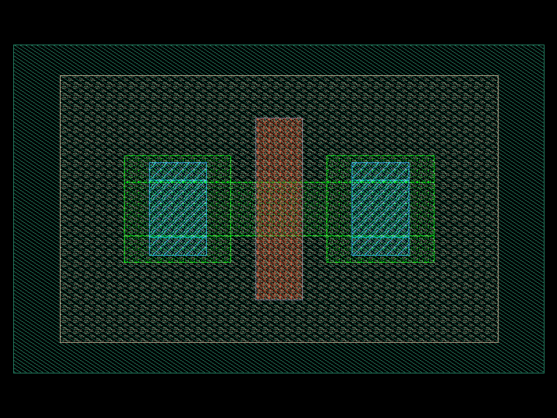
@gf.cell(schematic_function=pmos_schematic, tags=["IHP", "mos", "lv"])
def pmos(
    width: float = 0.15,
    length: float = 0.13,
    nf: int = 1,
    m: int = 1,
    model: str = "sg13_lv_pmos",
) -> Component:
    """Create a PMOS transistor.

    Args:
        width: Total width of the transistor in micrometers.
        length: Gate length in micrometers.
        nf: Number of fingers.
        m: Multiplier (number of parallel devices).
        model: Device model name.

    Returns:
        Component with PMOS transistor layout.

    Raises:
        ValueError: If width, length, or nf is outside allowed range.
    """
    if width < TECH.pmos_min_width or width > TECH.pmos_max_width:
        raise ValueError(
            f"pmos width={width} out of range [{TECH.pmos_min_width}, {TECH.pmos_max_width}]"
        )
    if length < TECH.pmos_min_length or length > TECH.pmos_max_length:
        raise ValueError(
            f"pmos length={length} out of range [{TECH.pmos_min_length}, {TECH.pmos_max_length}]"
        )
    if nf < 1 or nf > TECH.pmos_max_nf:
        raise ValueError(f"pmos nf={nf} out of range [1, {TECH.pmos_max_nf}]")

    c = _mos_core(width, length, nf, is_pmos=True, is_hv=False)
    return c

pmos

import warnings
warnings.filterwarnings("ignore", category=DeprecationWarning)

from ihp import PDK
from ihp import cells

PDK.activate()

c = cells.pmos(width=0.15, length=0.13, nf=1, m=1, model='sg13_lv_pmos').copy()
c.draw_ports()
c.plot()

pmos_hv

Create a high-voltage PMOS transistor.

Parameters:

Name Type Description Default
width float

Total width of the transistor in micrometers.

0.3
length float

Gate length in micrometers.

0.4
nf int

Number of fingers.

1
m int

Multiplier (number of parallel devices).

1
model str

Device model name.

'sg13_hv_pmos'

Returns:

Type Description
Component

Component with HV PMOS transistor layout.

Raises:

Type Description
ValueError

If width, length, or nf is outside allowed range.

Source code in ihp/cells/fet_transistors.py
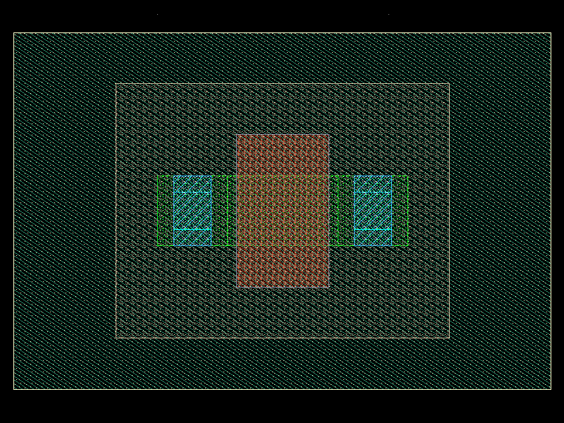
@gf.cell(schematic_function=pmos_hv_schematic, tags=["IHP", "mos", "hv"])
def pmos_hv(
    width: float = 0.30,
    length: float = 0.40,
    nf: int = 1,
    m: int = 1,
    model: str = "sg13_hv_pmos",
) -> Component:
    """Create a high-voltage PMOS transistor.

    Args:
        width: Total width of the transistor in micrometers.
        length: Gate length in micrometers.
        nf: Number of fingers.
        m: Multiplier (number of parallel devices).
        model: Device model name.

    Returns:
        Component with HV PMOS transistor layout.

    Raises:
        ValueError: If width, length, or nf is outside allowed range.
    """
    if width < TECH.pmos_hv_min_width or width > TECH.pmos_hv_max_width:
        raise ValueError(
            f"pmos_hv width={width} out of range [{TECH.pmos_hv_min_width}, {TECH.pmos_hv_max_width}]"
        )
    if length < TECH.pmos_hv_min_length or length > TECH.pmos_hv_max_length:
        raise ValueError(
            f"pmos_hv length={length} out of range [{TECH.pmos_hv_min_length}, {TECH.pmos_hv_max_length}]"
        )
    if nf < 1 or nf > TECH.pmos_hv_max_nf:
        raise ValueError(f"pmos_hv nf={nf} out of range [1, {TECH.pmos_hv_max_nf}]")

    c = _mos_core(width, length, nf, is_pmos=True, is_hv=True)
    return c

pmos_hv

import warnings
warnings.filterwarnings("ignore", category=DeprecationWarning)

from ihp import PDK
from ihp import cells

PDK.activate()

c = cells.pmos_hv(width=0.3, length=0.4, nf=1, m=1, model='sg13_hv_pmos').copy()
c.draw_ports()
c.plot()

pnpMPA

Returns the IHP pnpMPA BJT transistor as a gdsfactory Component.

This function generates a layout for a PNP transistor using the IHP process. The geometry of the transistor is defined by its width and length.

Parameters:

Name Type Description Default
length float

Length of the transistor, in microns.

2
width float

Width of the transistor, in microns.

0.7

Returns:

Type Description
Component

gdsfactory.Component: The generated pnpMPA transistor layout.

Raises:

Type Description
ValueError

If width or length is outside allowed range.

Source code in ihp/cells/bjt_transistors.py
2149
2150
2151
2152
2153
2154
2155
2156
2157
2158
2159
2160
2161
2162
2163
2164
2165
2166
2167
2168
2169
2170
2171
2172
2173
2174
2175
2176
2177
2178
2179
2180
2181
2182
2183
2184
2185
2186
2187
2188
2189
2190
2191
2192
2193
2194
2195
2196
2197
2198
2199
2200
2201
2202
2203
2204
2205
2206
2207
2208
2209
2210
2211
2212
2213
2214
2215
2216
2217
2218
2219
2220
2221
2222
2223
2224
2225
2226
2227
2228
2229
2230
2231
2232
2233
2234
2235
2236
2237
2238
2239
2240
2241
2242
2243
2244
2245
2246
2247
2248
2249
2250
2251
2252
2253
2254
2255
2256
2257
2258
2259
2260
2261
2262
2263
2264
2265
2266
2267
2268
2269
2270
2271
2272
2273
2274
2275
2276
2277
2278
2279
2280
2281
2282
2283
2284
2285
2286
2287
2288
2289
2290
2291
2292
2293
2294
2295
2296
2297
2298
2299
2300
2301
2302
2303
2304
2305
2306
2307
2308
2309
2310
2311
2312
2313
2314
2315
2316
2317
2318
2319
2320
2321
2322
2323
2324
2325
2326
2327
2328
2329
2330
2331
2332
2333
2334
2335
2336
2337
2338
2339
2340
2341
2342
2343
2344
2345
2346
2347
2348
2349
2350
2351
2352
2353
2354
2355
2356
2357
2358
2359
2360
2361
2362
2363
2364
2365
2366
2367
2368
2369
2370
2371
2372
2373
2374
2375
2376
2377
2378
2379
2380
2381
2382
2383
2384
2385
2386
2387
2388
2389
2390
2391
2392
2393
2394
2395
2396
2397
2398
2399
2400
2401
2402
2403
2404
2405
2406
2407
2408
2409
2410
2411
2412
2413
2414
2415
2416
2417
2418
2419
2420
2421
2422
2423
2424
2425
2426
2427
2428
2429
2430
2431
2432
2433
2434
2435
2436
2437
2438
2439
2440
2441
2442
2443
2444
2445
2446
2447
2448
2449
2450
2451
2452
2453
2454
2455
2456
2457
2458
2459
2460
2461
2462
2463
2464
2465
2466
2467
2468
2469
2470
2471
2472
2473
2474
2475
2476
2477
2478
2479
2480
2481
2482
2483
2484
2485
2486
2487
2488
2489
2490
2491
2492
2493
2494
2495
2496
2497
2498
2499
2500
2501
2502
2503
2504
2505
2506
2507
2508
2509
2510
2511
2512
2513
2514
2515
2516
2517
2518
2519
2520
2521
2522
2523
2524
2525
2526
2527
2528
2529
2530
2531
2532
2533
2534
2535
2536
2537
2538
2539
2540
2541
2542
2543
2544
2545
2546
2547
2548
2549
2550
2551
2552
2553
2554
2555
2556
2557
2558
2559
2560
2561
2562
2563
2564
2565
2566
2567
2568
2569
2570
2571
2572
2573
2574
2575
2576
2577
2578
2579
2580
2581
2582
2583
2584
2585
2586
2587
2588
2589
2590
2591
2592
2593
2594
2595
2596
2597
2598
2599
2600
2601
2602
2603
@gf.cell(schematic_function=pnpMPA_schematic, tags=["IHP", "bjt", "pnp"])
def pnpMPA(length: float = 2, width: float = 0.7) -> gf.Component:
    """Returns the IHP pnpMPA BJT transistor as a gdsfactory Component.

    This function generates a layout for a PNP transistor using the IHP process.
    The geometry of the transistor is defined by its width and length.

    Args:
        length: Length of the transistor, in microns.
        width: Width of the transistor, in microns.

    Returns:
        gdsfactory.Component: The generated pnpMPA transistor layout.

    Raises:
        ValueError: If width or length is outside allowed range.
    """
    if width < _TECH.pnp_min_width or width > _TECH.pnp_max_width:
        raise ValueError(
            f"pnpMPA width={width} out of range [{_TECH.pnp_min_width}, {_TECH.pnp_max_width}]"
        )
    if length < _TECH.pnp_min_length or length > _TECH.pnp_max_length:
        raise ValueError(
            f"pnpMPA length={length} out of range [{_TECH.pnp_min_length}, {_TECH.pnp_max_length}]"
        )

    c = gf.Component()

    SG13_GRID = _TECH.grid
    SG13_IGRID = 1.0 / SG13_GRID
    epsilon = _TECH.epsilon

    hact = (fix(length * SG13_IGRID + epsilon) * SG13_GRID) * 0.5
    wact = (fix(width * SG13_IGRID + epsilon) * SG13_GRID) * 0.5

    Cnt_a = _TECH.cont_size
    Cnt_b = _TECH.cont_spacing
    Cnt_b1 = _TECH.cont_b1
    M1_c1 = _TECH.m1_endcap
    pSD_c = _TECH.psd_activ_over

    w1m1 = wact - 0.02
    h1m1 = hact - 0.02
    wpsd = wact + 0.21
    hpsd = hact + 0.18
    w2act = wpsd + pSD_c
    h2act = hpsd + pSD_c
    dw2act = max(wact, 0.3)
    dh2act = 0.29
    w2m1 = w2act + 0.02
    h2m1 = h2act + 0.02
    dw2m1 = dw2act - 0.04
    dh2m1 = dh2act - 0.04
    wbulay = w2act + dw2act + 0.05
    hbulay = h2act + dh2act + 0.05
    wnwell = wbulay + 0.26
    hnwell = hbulay + 0.26
    w2psd = wnwell + 0.5
    h2psd = hnwell + 0.5
    d2psd = 0.75
    w3act = w2psd + 0.2
    h3act = h2psd + 0.2
    d3act = 0.35

    activLayer: LayerSpec = "Activdrawing"  # 1
    contLayer: LayerSpec = "Contdrawing"  # 6
    metal1Layer: LayerSpec = "Metal1drawing"  # 8
    metal1_pin_Layer: LayerSpec = "Metal1pin"  # 8
    pSdLayer: LayerSpec = "pSDdrawing"  # 14
    nwellLayer: LayerSpec = "NWelldrawing"  # 31
    nBuLayer: LayerSpec = "nBuLaydrawing"  # 32
    textLayer: LayerSpec = "TEXTdrawing"  # 63

    c.add_ref(
        gf.components.rectangle(size=(2 * wact, 2 * hact), layer=activLayer)
    ).move((-wact, -hact))

    # Labels
    c.add_label(
        text="PLUS",
        layer=textLayer,
    )

    c.add_label(
        text="MINUS",
        layer=textLayer,
        position=(-w2m1 - dw2m1 / 2, 0),
    )

    c.add_label(text="pnpMPA", layer=textLayer, position=(0, -(hnwell + h2psd) / 2))

    c.add_ref(gf.components.rectangle(size=(2 * wpsd, 2 * hpsd), layer=pSdLayer)).move(
        (-wpsd, -hpsd)
    )

    _xl = -w1m1
    _xh = w1m1
    _yl = -h1m1
    _yh = h1m1
    _ox = M1_c1
    _oy = M1_c1
    _ws = Cnt_a
    _ds = Cnt_b
    vg4 = (Cnt_a + Cnt_b) * 4 + Cnt_a + _ox * 2
    if _xh - _xl >= vg4 and _yh - _yl >= vg4:
        _ds = Cnt_b1

    contactArray(
        c,
        length=_xh - _xl,
        width=_yh - _yl,
        contactLayer=contLayer,
        xl=_xl,
        yl=_yl,
        ox=_ox,
        oy=_oy,
        ws=_ws,
        ds=_ds,
    )

    ref1 = c << gf.components.rectangle(size=(2 * w2act, 2 * h2act), layer=activLayer)
    ref1.move((-w2act, -h2act))

    ref2 = c << gf.components.rectangle(
        size=(2 * w2act + 2 * dw2act, 2 * h2act + 2 * dh2act), layer=activLayer
    )
    ref2.move((-w2act - dw2act, -h2act - dh2act))

    c.add_ref(
        gf.boolean(
            ref2,
            ref1,
            operation="xor",
            layer=activLayer,
            layer1=activLayer,
            layer2=activLayer,
        )
    )
    # Delete the rectangle that was covering the whole region
    ref1.delete()
    # Delete the inner rectangle used for boolean
    ref2.delete()

    # Metals
    ref1 = c << gf.components.rectangle(size=(2 * w2m1, 2 * h2m1), layer=metal1Layer)
    ref1.move((-w2m1, -h2m1))

    ref2 = c << gf.components.rectangle(
        size=(2 * w2m1 + 2 * dw2m1, 2 * h2m1 + 2 * dh2m1), layer=metal1Layer
    )
    ref2.move((-w2m1 - dw2m1, -h2m1 - dh2m1))

    c.add_ref(
        gf.boolean(
            ref2,
            ref1,
            operation="xor",
            layer=metal1Layer,
            layer1=metal1Layer,
            layer2=metal1Layer,
        )
    )
    # Delete the rectangle that was covering the whole region
    ref1.delete()
    # Delete the inner rectangle used for boolean
    ref2.delete()

    _xl = -w2m1 - dw2m1
    _xh = -w2m1
    _yl = -h2m1
    _yh = h2m1
    if _xh - _xl >= vg4 and _yh - _yl >= vg4:
        _ds = Cnt_b1

    contactArray(
        c,
        length=_xh - _xl,
        width=_yh - _yl,
        contactLayer=contLayer,
        xl=_xl,
        yl=_yl,
        ox=_ox,
        oy=_oy,
        ws=_ws,
        ds=_ds,
    )
    _xl = w2m1
    _xh = w2m1 + dw2m1
    contactArray(
        c,
        length=_xh - _xl,
        width=_yh - _yl,
        contactLayer=contLayer,
        xl=_xl,
        yl=_yl,
        ox=_ox,
        oy=_oy,
        ws=_ws,
        ds=_ds,
    )

    c.add_ref(
        gf.components.rectangle(size=(2 * wbulay, 2 * hbulay), layer=nBuLayer)
    ).move((-wbulay, -hbulay))

    c.add_ref(
        gf.components.rectangle(size=(2 * wnwell, 2 * hnwell), layer=nwellLayer)
    ).move((-wnwell, -hnwell))

    # Ring
    ref1 = c << gf.components.rectangle(size=(2 * w2psd, 2 * h2psd), layer=pSdLayer)
    ref1.move((-w2psd, -h2psd))

    ref2 = c << gf.components.rectangle(
        size=(2 * w2psd + 2 * d2psd, 2 * h2psd + 2 * d2psd), layer=pSdLayer
    )
    ref2.move((-w2psd - d2psd, -h2psd - d2psd))

    c.add_ref(
        gf.boolean(
            ref2,
            ref1,
            operation="xor",
            layer=pSdLayer,
            layer1=pSdLayer,
            layer2=pSdLayer,
        )
    )
    # Delete the rectangle that was covering the whole region
    ref1.delete()
    # Delete the inner rectangle used for boolean
    ref2.delete()

    ref1 = c << gf.components.rectangle(size=(2 * w3act, 2 * h3act), layer=activLayer)
    ref1.move((-w3act, -h3act))

    ref2 = c << gf.components.rectangle(
        size=(2 * w3act + 2 * d3act, 2 * h3act + 2 * d3act), layer=activLayer
    )
    ref2.move((-w3act - d3act, -h3act - d3act))

    c.add_ref(
        gf.boolean(
            ref2,
            ref1,
            operation="xor",
            layer=activLayer,
            layer1=activLayer,
            layer2=activLayer,
        )
    )
    # Delete the rectangle that was covering the whole region
    ref1.delete()
    # Delete the inner rectangle used for boolean
    ref2.delete()

    ref1 = c << gf.components.rectangle(size=(2 * w3act, 2 * h3act), layer=metal1Layer)
    ref1.move((-w3act, -h3act))

    ref2 = c << gf.components.rectangle(
        size=(2 * w3act + 2 * d3act, 2 * h3act + 2 * d3act), layer=metal1Layer
    )
    ref2.move((-w3act - d3act, -h3act - d3act))

    c.add_ref(
        gf.boolean(
            ref2,
            ref1,
            operation="xor",
            layer=metal1Layer,
            layer1=metal1Layer,
            layer2=metal1Layer,
        )
    )
    # Delete the rectangle that was covering the whole region
    ref1.delete()
    # Delete the inner rectangle used for boolean
    ref2.delete()

    # Ring Metal
    MetT = True  # include pins on top
    MetB = True  # include pins on bottom
    MetL = True  # include pins left
    MetR = True  # include pins right
    _ds = Cnt_b
    _ox = 0.095
    idtie = 0

    if MetT:
        _xl = -w3act - d3act
        _xh = w3act + d3act
        _yl = h3act
        _yh = h3act + d3act
        contactArray(
            c,
            length=_xh - _xl,
            width=_yh - _yl,
            contactLayer=contLayer,
            xl=_xl,
            yl=_yl,
            ox=_ox,
            oy=_oy,
            ws=_ws,
            ds=_ds,
        )
        if idtie == 0:
            # Assigning reference to idtie, so that it is not used again in the next if statements.
            idtie = c << gf.components.rectangle(
                size=(2 * (w3act + d3act), d3act), layer=metal1_pin_Layer
            )
            idtie.move((-w3act - d3act, h3act))

            # Coordinates to be used for port
            idtie_xmin = -w3act - d3act
            idtie_xmax = idtie_xmin + 2 * (w3act + d3act)
            idtie_ymin = h3act
            idtie_ymax = idtie_ymin + d3act

            c.add_label(text="TIE", layer=textLayer, position=(0, h3act + d3act / 2))

    if MetB:
        _xl = -w3act - d3act
        _xh = w3act + d3act
        _yl = -h3act - d3act
        _yh = -h3act
        contactArray(
            c,
            length=_xh - _xl,
            width=_yh - _yl,
            contactLayer=contLayer,
            xl=_xl,
            yl=_yl,
            ox=_ox,
            oy=_oy,
            ws=_ws,
            ds=_ds,
        )
        if idtie == 0:
            idtie = c << gf.components.rectangle(
                size=(2 * (w3act + d3act), d3act), layer=metal1_pin_Layer
            )
            idtie.move((-w3act - d3act, -h3act - d3act))

            # Coordinates to be used for port
            idtie_xmin = -w3act - d3act
            idtie_xmax = idtie_xmin + 2 * (w3act + d3act)
            idtie_ymin = -h3act - d3act
            idtie_ymax = idtie_ymin + d3act

            c.add_label(text="TIE", layer=textLayer, position=(0, -h3act - d3act / 2))

    _oy = 0.085
    if MetL:
        _xl = -w3act - d3act
        _xh = -w3act
        _yl = -h3act
        _yh = h3act
        contactArray(
            c,
            length=_xh - _xl,
            width=_yh - _yl,
            contactLayer=contLayer,
            xl=_xl,
            yl=_yl,
            ox=_ox,
            oy=_oy,
            ws=_ws,
            ds=_ds,
        )
        if idtie == 0:
            idtie = c << gf.components.rectangle(
                size=(d3act, 2 * h3act), layer=metal1_pin_Layer
            )
            idtie.move((-w3act - d3act, -h3act))

            # Coordinates to be used for port
            idtie_xmin = -w3act - d3act
            idtie_xmax = idtie_xmin + d3act
            idtie_ymin = -h3act
            idtie_ymax = idtie_ymin + 2 * h3act

            c.add_label(text="TIE", layer=textLayer, position=(-w3act - d3act / 2, 0))

    if MetR:
        _xl = w3act
        _xh = w3act + d3act
        _yl = -h3act
        _yh = h3act
        contactArray(
            c,
            length=_xh - _xl,
            width=_yh - _yl,
            contactLayer=contLayer,
            xl=_xl,
            yl=_yl,
            ox=_ox,
            oy=_oy,
            ws=_ws,
            ds=_ds,
        )
        if idtie == 0:
            idtie = c << gf.components.rectangle(
                size=(d3act, 2 * h3act), layer=metal1_pin_Layer
            )
            idtie.move((w3act, -h3act))

            # Coordinates to be used for port
            idtie_xmin = w3act
            idtie_xmax = idtie_xmin + d3act
            idtie_ymin = -h3act
            idtie_ymax = idtie_ymin + 2 * h3act

            c.add_label(text="TIE", layer=textLayer, position=(w3act + d3act / 2, 0))

    c.add_ref(
        gf.components.rectangle(size=(2 * w1m1, 2 * h1m1), layer=metal1_pin_Layer)
    ).move((-w1m1, -h1m1))

    c.add_ref(
        gf.components.rectangle(size=(2 * w1m1, 2 * h1m1), layer=metal1Layer)
    ).move((-w1m1, -h1m1))

    c.add_ref(
        gf.components.rectangle(size=(dw2m1, 2 * h2m1), layer=metal1_pin_Layer)
    ).move((-w2m1 - dw2m1, -h2m1))

    if idtie != 0:
        c.add_port(
            "TIE",
            center=(0.5 * (idtie_xmin + idtie_xmax), 0.5 * (idtie_ymin + idtie_ymax)),
            width=_snap_width_to_grid(idtie_ymax - idtie_ymin),
            layer=metal1_pin_Layer,
            orientation=180.0,
            port_type="electrical",
        )

    c.add_port(
        "PLUS",
        center=(0, 0),
        width=_snap_width_to_grid(2 * w1m1),
        layer=metal1_pin_Layer,
        orientation=270.0,
        port_type="electrical",
    )

    c.add_port(
        "MINUS",
        center=(-w2m1 - dw2m1 / 2, 0),
        width=_snap_width_to_grid(dw2m1),
        layer=metal1_pin_Layer,
        orientation=270.0,
        port_type="electrical",
    )

    return c

pnpMPA

import warnings
warnings.filterwarnings("ignore", category=DeprecationWarning)

from ihp import PDK
from ihp import cells

PDK.activate()

c = cells.pnpMPA(length=2, width=0.7).copy()
c.draw_ports()
c.plot()

ptap1

Create a P+ substrate tap.

Parameters:

Name Type Description Default
width float

Width of the tap in micrometers.

1.0
length float

Length of the tap in micrometers.

1.0
rows int

Number of contact rows.

1
cols int

Number of contact columns.

1
layer_activ tuple[int, int] | str | int | LayerEnum

Active region layer.

'Activdrawing'
layer_psd tuple[int, int] | str | int | LayerEnum

P+ source/drain doping layer.

'pSDdrawing'
layer_cont tuple[int, int] | str | int | LayerEnum

Contact layer.

'Contdrawing'
layer_metal1 tuple[int, int] | str | int | LayerEnum

Metal1 layer.

'Metal1drawing'

Returns:

Type Description
Component

Component with P+ tap layout.

Raises:

Type Description
ValueError

If width or length is outside allowed range.

Source code in ihp/cells/passives.py
@gf.cell(schematic_function=ptap1_schematic, tags=["IHP", "tap", "p-type"])
def ptap1(
    width: float = 1.0,
    length: float = 1.0,
    rows: int = 1,
    cols: int = 1,
    layer_activ: LayerSpec = "Activdrawing",
    layer_psd: LayerSpec = "pSDdrawing",
    layer_cont: LayerSpec = "Contdrawing",
    layer_metal1: LayerSpec = "Metal1drawing",
    layer_metal1_pin: LayerSpec = "Metal1pin",
) -> Component:
    """Create a P+ substrate tap.

    Args:
        width: Width of the tap in micrometers.
        length: Length of the tap in micrometers.
        rows: Number of contact rows.
        cols: Number of contact columns.
        layer_activ: Active region layer.
        layer_psd: P+ source/drain doping layer.
        layer_cont: Contact layer.
        layer_metal1: Metal1 layer.

    Returns:
        Component with P+ tap layout.

    Raises:
        ValueError: If width or length is outside allowed range.
    """
    if width < tech.TECH.ptap1_min_size or width > tech.TECH.ptap1_max_size:
        raise ValueError(
            f"ptap1 width={width} out of range [{tech.TECH.ptap1_min_size}, {tech.TECH.ptap1_max_size}]"
        )
    if length < tech.TECH.ptap1_min_size or length > tech.TECH.ptap1_max_size:
        raise ValueError(
            f"ptap1 length={length} out of range [{tech.TECH.ptap1_min_size}, {tech.TECH.ptap1_max_size}]"
        )

    c = Component()

    # Design rules
    cont_size = 0.16
    cont_spacing = 0.18
    metal_enc = 0.06
    tap_enc = 0.1

    # Grid snap
    grid = 0.005
    width = round(width / grid) * grid
    length = round(length / grid) * grid

    # P+ active region
    active = gf.components.rectangle(
        size=(length, width),
        layer=layer_activ,
        centered=True,
    )
    c.add_ref(active)

    # P+ implant
    psd = gf.components.rectangle(
        size=(length + 2 * tap_enc, width + 2 * tap_enc),
        layer=layer_psd,
        centered=True,
    )
    c.add_ref(psd)

    # Contact array
    cont_array_width = cont_size * cols + cont_spacing * (cols - 1)
    cont_array_height = cont_size * rows + cont_spacing * (rows - 1)

    for i in range(cols):
        for j in range(rows):
            x = -cont_array_width / 2 + cont_size / 2 + i * (cont_size + cont_spacing)
            y = -cont_array_height / 2 + cont_size / 2 + j * (cont_size + cont_spacing)

            cont = gf.components.rectangle(
                size=(cont_size, cont_size),
                layer=layer_cont,
                centered=True,
            )
            cont_ref = c.add_ref(cont)
            cont_ref.move((x, y))

    # Metal1 connection
    metal = gf.components.rectangle(
        size=(cont_array_width + 2 * metal_enc, cont_array_height + 2 * metal_enc),
        layer=layer_metal1,
        centered=True,
    )
    c.add_ref(metal)

    # Add port
    c.add_port(
        name="TAP",
        center=(0, 0),
        width=width,
        orientation=0,
        layer=layer_metal1_pin,
        port_type="electrical",
    )

    # Add metadata
    c.info["type"] = "ptap"
    c.info["width"] = width
    c.info["length"] = length
    c.info["rows"] = rows
    c.info["cols"] = cols

    return c

ptap1

import warnings
warnings.filterwarnings("ignore", category=DeprecationWarning)

from ihp import PDK
from ihp import cells

PDK.activate()

c = cells.ptap1(width=1.0, length=1.0, rows=1, cols=1, layer_activ='Activdrawing', layer_psd='pSDdrawing', layer_cont='Contdrawing', layer_metal1='Metal1drawing', layer_metal1_pin='Metal1pin').copy()
c.draw_ports()
c.plot()

quarter_wave_transformer

Returns a quarter-wave transformer coplanar transmission line.

Creates a quarter-wave transformer for impedance matching between an input impedance Z_in and a load impedance Z_L at a given frequency.

Parameters:

Name Type Description Default
connection_length float

Length of the input line.

100
frequency float

Operating frequency (Hz).

50000000000.0
Z_in float

Characteristic impedance of the input line (ohms).

50
Z_L float

Load impedance to be matched (ohms).

100
signal_cross_section CrossSection | str | dict[str, Any] | Callable[..., CrossSection] | SymmetricalCrossSection | DCrossSection

Cross-section for the signal line.

'topmetal2_routing'
ground_cross_section CrossSection | str | dict[str, Any] | Callable[..., CrossSection] | SymmetricalCrossSection | DCrossSection

Cross-section for the ground line.

'topmetal1_routing'
e_r float

Relative permittivity of the substrate. Defaults to 4.1 for silicon dioxide.

4.1
Source code in ihp/cells/rf_devices.py
@gf.cell
def quarter_wave_transformer(
    connection_length: float = 100,
    frequency: float = 50e9,
    Z_in: float = 50,
    Z_L: float = 100,
    signal_cross_section: CrossSectionSpec = "topmetal2_routing",
    ground_cross_section: CrossSectionSpec = "topmetal1_routing",
    e_r: float = 4.1,
) -> gf.Component:
    """Returns a quarter-wave transformer coplanar transmission line.

    Creates a quarter-wave transformer for impedance matching between an
    input impedance Z_in and a load impedance Z_L at a given frequency.

    Args:
        connection_length: Length of the input line.
        frequency: Operating frequency (Hz).
        Z_in: Characteristic impedance of the input line (ohms).
        Z_L: Load impedance to be matched (ohms).
        signal_cross_section: Cross-section for the signal line.
        ground_cross_section: Cross-section for the ground line.
        e_r: Relative permittivity of the substrate. Defaults to 4.1 for silicon dioxide.
    """
    wave_length = scipy.constants.c / frequency * 1e6

    c = gf.Component()

    e_eff = _calculate_effective_dielectric_constant(
        signal_cross_section=signal_cross_section,
        ground_cross_section=ground_cross_section,
        e_r=e_r,
    )

    quater_wave_length = wave_length / 4 / sqrt(e_eff)
    quater_wave_length = quater_wave_length - quater_wave_length % (
        tech.nm
    )  # truncate to 5 nm

    Z0_transformer = sqrt(Z_in * Z_L)

    transformer_line = c.add_ref(
        tline(
            length=quater_wave_length,
            Z0=Z0_transformer,
            signal_cross_section=signal_cross_section,
            ground_cross_section=ground_cross_section,
        )
    )

    connection_port1 = c.add_ref(
        tline(
            length=connection_length,
            Z0=Z_in,
            signal_cross_section=signal_cross_section,
            ground_cross_section=ground_cross_section,
        )
    )

    connection_port1.connect(
        "e1", transformer_line.ports["e1"], allow_width_mismatch=True
    )

    connection_port2 = c.add_ref(
        tline(
            length=connection_length,
            Z0=Z_L,
            signal_cross_section=signal_cross_section,
            ground_cross_section=ground_cross_section,
        )
    )

    connection_port2.connect(
        "e1", transformer_line.ports["e2"], allow_width_mismatch=True
    )

    c.add_port(name="e1", port=connection_port1.ports["e2"])
    c.add_port(name="e2", port=connection_port2.ports["e2"])

    return c

quarter_wave_transformer

import warnings
warnings.filterwarnings("ignore", category=DeprecationWarning)

from ihp import PDK
from ihp import cells

PDK.activate()

c = cells.quarter_wave_transformer(connection_length=100, frequency=50000000000.0, Z_in=50, Z_L=100, signal_cross_section='topmetal2_routing', ground_cross_section='topmetal1_routing', e_r=4.1).copy()
c.draw_ports()
c.plot()

rfcmim

Create a MIM (Metal-Insulator-Metal) capacitor isolated by a bulk charge-drift encapsulation P-Plus guard-ring.

Parameters:

Name Type Description Default
width float

Width of the capacitor in micrometers.

7.0
length float

Length of the capacitor in micrometers.

7.0
layer_metal5 tuple[int, int] | str | int | LayerEnum

Metal 5 drawing layer.

'Metal5drawing'
layer_mim tuple[int, int] | str | int | LayerEnum

MIM device drawing layer.

'MIMdrawing'
layer_vmim tuple[int, int] | str | int | LayerEnum

Vmim (MIM-TopMetal1 Via) drawing layer.

'Vmimdrawing'
layer_topmetal1 tuple[int, int] | str | int | LayerEnum

TopMetal1 drawing layer.

'TopMetal1drawing'
layer_cap_mark tuple[int, int] | str | int | LayerEnum

MemCap drawing layer.

'MemCapdrawing'
layer_m4nofill tuple[int, int] | str | int | LayerEnum

Metal4 nofill logic layer.

'Metal4nofill'
layer_m5nofill tuple[int, int] | str | int | LayerEnum

Metal5 nofill logic layer.

'Metal5nofill'
layer_tm1nofill tuple[int, int] | str | int | LayerEnum

TopMetal1 nofill logic layer.

'TopMetal1nofill'
layer_tm2nofill tuple[int, int] | str | int | LayerEnum

TopMetal2 nofill logic layer.

'TopMetal2nofill'
layer_text tuple[int, int] | str | int | LayerEnum

TEXT drawing layer.

'TEXTdrawing'
layer_metal5label tuple[int, int] | str | int | LayerEnum

Metal5 label logic layer.

'Metal5label'
layer_topmetal1label tuple[int, int] | str | int | LayerEnum

TopMetal1 label logic layer.

'TopMetal1label'
layer_metal5pin tuple[int, int] | str | int | LayerEnum

Metal5 pin logic layer.

'Metal5pin'
layer_topmetal1pin tuple[int, int] | str | int | LayerEnum

TopMetal1 pin logic layer.

'TopMetal1pin'
model str

Device model name.

'rfcmim'

Returns:

Type Description
Component

Component with MIM capacitor layout.

Raises:

Type Description
ValueError

If width or length is outside allowed range.

Source code in ihp/cells/capacitors.py
@gf.cell(schematic_function=rfcmim_schematic, tags=["IHP", "capacitor", "mim", "rf"])
def rfcmim(
    width: float = 7.0,
    length: float = 7.0,
    layer_pwellblock: LayerSpec = "PWellblock",
    layer_metal5: LayerSpec = "Metal5drawing",
    layer_mim: LayerSpec = "MIMdrawing",
    layer_vmim: LayerSpec = "Vmimdrawing",
    layer_topmetal1: LayerSpec = "TopMetal1drawing",
    layer_cap_mark: LayerSpec = "MemCapdrawing",
    layer_m4nofill: LayerSpec = "Metal4nofill",
    layer_m5nofill: LayerSpec = "Metal5nofill",
    layer_tm1nofill: LayerSpec = "TopMetal1nofill",
    layer_tm2nofill: LayerSpec = "TopMetal2nofill",
    layer_activ: LayerSpec = "Activdrawing",
    layer_cont: LayerSpec = "Contdrawing",
    layer_metal1: LayerSpec = "Metal1drawing",
    layer_psd: LayerSpec = "pSDdrawing",
    # layer_rfpad: LayerSpec = "RFPaddrawing",
    layer_activnoqrc: LayerSpec = "Activnoqrc",
    layer_metal1noqrc: LayerSpec = "Metal1noqrc",
    layer_metal2noqrc: LayerSpec = "Metal2noqrc",
    layer_metal3noqrc: LayerSpec = "Metal3noqrc",
    layer_metal4noqrc: LayerSpec = "Metal4noqrc",
    layer_metal5noqrc: LayerSpec = "Metal5noqrc",
    layer_topmetal1noqrc: LayerSpec = "TopMetal1noqrc",
    layer_text: LayerSpec = "TEXTdrawing",
    layer_metal1pin: LayerSpec = "Metal1pin",
    layer_metal5pin: LayerSpec = "Metal5pin",
    layer_topmetal1pin: LayerSpec = "TopMetal1pin",
    layer_metal5label: LayerSpec = "Metal5label",
    layer_topmetal1label: LayerSpec = "TopMetal1label",
    layer_metal1label: LayerSpec = "Metal1label",
    model: str = "rfcmim",
) -> Component:
    """Create a MIM (Metal-Insulator-Metal) capacitor isolated by a
    bulk charge-drift encapsulation P-Plus guard-ring.

    Args:
        width: Width of the capacitor in micrometers.
        length: Length of the capacitor in micrometers.

        layer_metal5: Metal 5 drawing layer.
        layer_mim: MIM device drawing layer.
        layer_vmim: Vmim (MIM-TopMetal1 Via) drawing layer.
        layer_topmetal1: TopMetal1 drawing layer.
        layer_cap_mark: MemCap drawing layer.
        layer_m4nofill: Metal4 nofill logic layer.
        layer_m5nofill: Metal5 nofill logic layer.
        layer_tm1nofill: TopMetal1 nofill logic layer.
        layer_tm2nofill: TopMetal2 nofill logic layer.
        layer_text: TEXT drawing layer.
        layer_metal5label: Metal5 label logic layer.
        layer_topmetal1label: TopMetal1 label logic layer.
        layer_metal5pin: Metal5 pin logic layer.
        layer_topmetal1pin: TopMetal1 pin logic layer.

        model: Device model name.

    Returns:
        Component with MIM capacitor layout.

    Raises:
        ValueError: If width or length is outside allowed range.
    """
    if width < tech.TECH.rfcmim_min_size or width > tech.TECH.rfcmim_max_size:
        raise ValueError(
            f"rfcmim width={width} out of range [{tech.TECH.rfcmim_min_size}, {tech.TECH.rfcmim_max_size}]"
        )
    if length < tech.TECH.rfcmim_min_size or length > tech.TECH.rfcmim_max_size:
        raise ValueError(
            f"rfcmim length={length} out of range [{tech.TECH.rfcmim_min_size}, {tech.TECH.rfcmim_max_size}]"
        )

    c = Component()

    cap = cmim(
        width=width,
        length=length,
        layer_metal5=layer_metal5,
        layer_mim=layer_mim,
        layer_vmim=layer_vmim,
        layer_topmetal1=layer_topmetal1,
        layer_cap_mark=layer_cap_mark,
        layer_m4nofill=layer_m4nofill,
        layer_m5nofill=layer_m5nofill,
        layer_tm1nofill=layer_tm1nofill,
        layer_tm2nofill=layer_tm2nofill,
        layer_text=layer_text,
        layer_metal5pin=layer_metal5pin,
        layer_topmetal1pin=layer_topmetal1pin,
        layer_metal5label=layer_metal5label,
        layer_topmetal1label=layer_topmetal1label,
        model=model,
    )
    c.info = cap.info
    c.info["model"] = "cap_rfcmim"
    c.add_ref(cap)
    c.ports = cap.ports
    # add pwell block
    size = c.bbox_np()
    size = size[1] - size[0]
    pwellblock_enc = 2.4
    pwell = gf.components.rectangle(
        size=(size[0] + 2 * pwellblock_enc, size[1] + 2 * pwellblock_enc),
        layer=layer_pwellblock,
        centered=True,
    )
    ccenter = (c.x, c.y)
    pwell_ref = c.add_ref(pwell)
    pwell_ref.x = ccenter[0]
    pwell_ref.y = ccenter[1]

    # add p guard ring
    pguardring_seq = 0.6
    pguardring_width = 2.0
    c.add_ref(
        guard_ring(
            width=pguardring_width,
            guardRingSpacing=pguardring_seq,
            guardRingType="psub",
            bbox=tuple(tuple(p) for p in c.bbox_np()),
            path=None,
            layer_activ=layer_activ,
            layer_cont=layer_cont,
            layer_metal1=layer_metal1,
            layer_psd=layer_psd,
        )
    )

    logic_layers = [
        layer_activnoqrc,
        layer_metal1noqrc,
        layer_metal2noqrc,
        layer_metal3noqrc,
        layer_metal4noqrc,
        layer_metal5noqrc,
        layer_topmetal1noqrc,
    ]

    size = c.bbox_np()
    size = size[1] - size[0]
    ccenter = (c.x, c.y)
    for layer_spec in logic_layers:
        ll = gf.components.rectangle(
            size=(size[0], size[1]),
            layer=layer_spec,
            centered=True,
        )
        ref = c.add_ref(ll)
        ref.x = ccenter[0]
        ref.y = ccenter[1]

    gr_drc = {
        "active_min_enclose_pp": 0.14,
    }

    # add TIE LOW pin
    tie_low = gf.components.rectangle(
        size=(size[0] - 2 * gr_drc["active_min_enclose_pp"], pguardring_width),
        layer=layer_metal1pin,
        centered=True,
    )
    xmin, ymin = c.xmin, c.ymin
    tie_low_ref = c.add_ref(tie_low)
    tie_low_ref.xmin = xmin + gr_drc["active_min_enclose_pp"]
    tie_low_ref.ymin = ymin + gr_drc["active_min_enclose_pp"]

    tie = c.add_port(
        name="TIE_LOW",
        center=(tie_low_ref.x, tie_low_ref.y),
        width=pguardring_width,
        orientation=0,
        layer=layer_metal1pin,
        port_type="electrical",
    )
    c.add_label(text="TIE_LOW", position=(tie.x, tie.y), layer=layer_metal1label)
    c.add_label(text="TIE_LOW", position=(tie.x, tie.y), layer=layer_text)

    return c

rfcmim

import warnings
warnings.filterwarnings("ignore", category=DeprecationWarning)

from ihp import PDK
from ihp import cells

PDK.activate()

c = cells.rfcmim(width=7.0, length=7.0, layer_pwellblock='PWellblock', layer_metal5='Metal5drawing', layer_mim='MIMdrawing', layer_vmim='Vmimdrawing', layer_topmetal1='TopMetal1drawing', layer_cap_mark='MemCapdrawing', layer_m4nofill='Metal4nofill', layer_m5nofill='Metal5nofill', layer_tm1nofill='TopMetal1nofill', layer_tm2nofill='TopMetal2nofill', layer_activ='Activdrawing', layer_cont='Contdrawing', layer_metal1='Metal1drawing', layer_psd='pSDdrawing', layer_activnoqrc='Activnoqrc', layer_metal1noqrc='Metal1noqrc', layer_metal2noqrc='Metal2noqrc', layer_metal3noqrc='Metal3noqrc', layer_metal4noqrc='Metal4noqrc', layer_metal5noqrc='Metal5noqrc', layer_topmetal1noqrc='TopMetal1noqrc', layer_text='TEXTdrawing', layer_metal1pin='Metal1pin', layer_metal5pin='Metal5pin', layer_topmetal1pin='TopMetal1pin', layer_metal5label='Metal5label', layer_topmetal1label='TopMetal1label', layer_metal1label='Metal1label', model='rfcmim').copy()
c.draw_ports()
c.plot()

rfnmos

Create an RF NMOS transistor.

Parameters:

Name Type Description Default
width float

Total width of the transistor in micrometers.

1.0
length float

Gate length in micrometers.

0.13
nf int

Number of fingers.

1
m int

Multiplier (number of parallel devices).

1
cnt_rows int

Number of contact rows.

1
met2_cont bool

Include Metal2-to-contact connections.

True
gat_ring bool

Include gate ring around the transistor.

True
guard_ring str

Guard ring type: "Yes", "No", "U", or "Top+Bottom".

'Yes'
model str

Device model name.

'sg13_lv_nmos'

Returns:

Type Description
Component

Component with RF NMOS transistor layout.

Raises:

Type Description
ValueError

If width, length, or nf is outside allowed range.

Source code in ihp/cells/rf_transistors.py
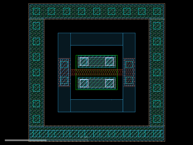
@gf.cell(schematic_function=rfnmos_schematic, tags=["IHP", "mos", "lv", "rf"])
def rfnmos(
    width: float = 1.0,
    length: float = 0.13,
    nf: int = 1,
    m: int = 1,
    cnt_rows: int = 1,
    met2_cont: bool = True,
    gat_ring: bool = True,
    guard_ring: str = "Yes",
    model: str = "sg13_lv_nmos",
) -> Component:
    """Create an RF NMOS transistor.

    Args:
        width: Total width of the transistor in micrometers.
        length: Gate length in micrometers.
        nf: Number of fingers.
        m: Multiplier (number of parallel devices).
        cnt_rows: Number of contact rows.
        met2_cont: Include Metal2-to-contact connections.
        gat_ring: Include gate ring around the transistor.
        guard_ring: Guard ring type: "Yes", "No", "U", or "Top+Bottom".
        model: Device model name.

    Returns:
        Component with RF NMOS transistor layout.

    Raises:
        ValueError: If width, length, or nf is outside allowed range.
    """
    if width < TECH.rfnmos_min_width or width > TECH.rfnmos_max_width:
        raise ValueError(
            f"rfnmos width={width} out of range [{TECH.rfnmos_min_width}, {TECH.rfnmos_max_width}]"
        )
    if length < TECH.rfnmos_min_length or length > TECH.rfnmos_max_length:
        raise ValueError(
            f"rfnmos length={length} out of range [{TECH.rfnmos_min_length}, {TECH.rfnmos_max_length}]"
        )
    if nf < 1 or nf > TECH.rfnmos_max_nf:
        raise ValueError(f"rfnmos nf={nf} out of range [1, {TECH.rfnmos_max_nf}]")

    c = _rf_mos_core(
        width,
        length,
        nf,
        cnt_rows,
        met2_cont,
        gat_ring,
        guard_ring,
        is_pmos=False,
        is_hv=False,
    )
    return c

rfnmos

import warnings
warnings.filterwarnings("ignore", category=DeprecationWarning)

from ihp import PDK
from ihp import cells

PDK.activate()

c = cells.rfnmos(width=1.0, length=0.13, nf=1, m=1, cnt_rows=1, met2_cont=True, gat_ring=True, guard_ring='Yes', model='sg13_lv_nmos').copy()
c.draw_ports()
c.plot()

rfnmos_hv

Create a high-voltage RF NMOS transistor.

Parameters:

Name Type Description Default
width float

Total width of the transistor in micrometers.

1.0
length float

Gate length in micrometers.

0.45
nf int

Number of fingers.

1
m int

Multiplier (number of parallel devices).

1
cnt_rows int

Number of contact rows.

1
met2_cont bool

Include Metal2-to-contact connections.

True
gat_ring bool

Include gate ring around the transistor.

True
guard_ring str

Guard ring type: "Yes", "No", "U", or "Top+Bottom".

'Yes'
model str

Device model name.

'sg13_hv_nmos'

Returns:

Type Description
Component

Component with HV RF NMOS transistor layout.

Raises:

Type Description
ValueError

If width, length, or nf is outside allowed range.

Source code in ihp/cells/rf_transistors.py
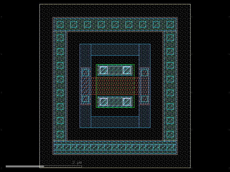
@gf.cell(schematic_function=rfnmos_hv_schematic, tags=["IHP", "mos", "hv", "rf"])
def rfnmos_hv(
    width: float = 1.0,
    length: float = 0.45,
    nf: int = 1,
    m: int = 1,
    cnt_rows: int = 1,
    met2_cont: bool = True,
    gat_ring: bool = True,
    guard_ring: str = "Yes",
    model: str = "sg13_hv_nmos",
) -> Component:
    """Create a high-voltage RF NMOS transistor.

    Args:
        width: Total width of the transistor in micrometers.
        length: Gate length in micrometers.
        nf: Number of fingers.
        m: Multiplier (number of parallel devices).
        cnt_rows: Number of contact rows.
        met2_cont: Include Metal2-to-contact connections.
        gat_ring: Include gate ring around the transistor.
        guard_ring: Guard ring type: "Yes", "No", "U", or "Top+Bottom".
        model: Device model name.

    Returns:
        Component with HV RF NMOS transistor layout.

    Raises:
        ValueError: If width, length, or nf is outside allowed range.
    """
    if width < TECH.rfnmos_hv_min_width or width > TECH.rfnmos_hv_max_width:
        raise ValueError(
            f"rfnmos_hv width={width} out of range [{TECH.rfnmos_hv_min_width}, {TECH.rfnmos_hv_max_width}]"
        )
    if length < TECH.rfnmos_hv_min_length or length > TECH.rfnmos_hv_max_length:
        raise ValueError(
            f"rfnmos_hv length={length} out of range [{TECH.rfnmos_hv_min_length}, {TECH.rfnmos_hv_max_length}]"
        )
    if nf < 1 or nf > TECH.rfnmos_hv_max_nf:
        raise ValueError(f"rfnmos_hv nf={nf} out of range [1, {TECH.rfnmos_hv_max_nf}]")

    c = _rf_mos_core(
        width,
        length,
        nf,
        cnt_rows,
        met2_cont,
        gat_ring,
        guard_ring,
        is_pmos=False,
        is_hv=True,
    )
    return c

rfnmos_hv

import warnings
warnings.filterwarnings("ignore", category=DeprecationWarning)

from ihp import PDK
from ihp import cells

PDK.activate()

c = cells.rfnmos_hv(width=1.0, length=0.45, nf=1, m=1, cnt_rows=1, met2_cont=True, gat_ring=True, guard_ring='Yes', model='sg13_hv_nmos').copy()
c.draw_ports()
c.plot()

rfpmos

Create an RF PMOS transistor.

Parameters:

Name Type Description Default
width float

Total width of the transistor in micrometers.

1.0
length float

Gate length in micrometers.

0.13
nf int

Number of fingers.

1
m int

Multiplier (number of parallel devices).

1
cnt_rows int

Number of contact rows.

1
met2_cont bool

Include Metal2-to-contact connections.

True
gat_ring bool

Include gate ring around the transistor.

True
guard_ring str

Guard ring type: "Yes", "No", "U", or "Top+Bottom".

'Yes'
model str

Device model name.

'sg13_lv_pmos'

Returns:

Type Description
Component

Component with RF PMOS transistor layout.

Raises:

Type Description
ValueError

If width, length, or nf is outside allowed range.

Source code in ihp/cells/rf_transistors.py
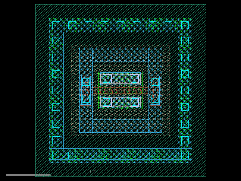
@gf.cell(schematic_function=rfpmos_schematic, tags=["IHP", "mos", "lv", "rf"])
def rfpmos(
    width: float = 1.0,
    length: float = 0.13,
    nf: int = 1,
    m: int = 1,
    cnt_rows: int = 1,
    met2_cont: bool = True,
    gat_ring: bool = True,
    guard_ring: str = "Yes",
    model: str = "sg13_lv_pmos",
) -> Component:
    """Create an RF PMOS transistor.

    Args:
        width: Total width of the transistor in micrometers.
        length: Gate length in micrometers.
        nf: Number of fingers.
        m: Multiplier (number of parallel devices).
        cnt_rows: Number of contact rows.
        met2_cont: Include Metal2-to-contact connections.
        gat_ring: Include gate ring around the transistor.
        guard_ring: Guard ring type: "Yes", "No", "U", or "Top+Bottom".
        model: Device model name.

    Returns:
        Component with RF PMOS transistor layout.

    Raises:
        ValueError: If width, length, or nf is outside allowed range.
    """
    if width < TECH.rfpmos_min_width or width > TECH.rfpmos_max_width:
        raise ValueError(
            f"rfpmos width={width} out of range [{TECH.rfpmos_min_width}, {TECH.rfpmos_max_width}]"
        )
    if length < TECH.rfpmos_min_length or length > TECH.rfpmos_max_length:
        raise ValueError(
            f"rfpmos length={length} out of range [{TECH.rfpmos_min_length}, {TECH.rfpmos_max_length}]"
        )
    if nf < 1 or nf > TECH.rfpmos_max_nf:
        raise ValueError(f"rfpmos nf={nf} out of range [1, {TECH.rfpmos_max_nf}]")

    c = _rf_mos_core(
        width,
        length,
        nf,
        cnt_rows,
        met2_cont,
        gat_ring,
        guard_ring,
        is_pmos=True,
        is_hv=False,
    )
    return c

rfpmos

import warnings
warnings.filterwarnings("ignore", category=DeprecationWarning)

from ihp import PDK
from ihp import cells

PDK.activate()

c = cells.rfpmos(width=1.0, length=0.13, nf=1, m=1, cnt_rows=1, met2_cont=True, gat_ring=True, guard_ring='Yes', model='sg13_lv_pmos').copy()
c.draw_ports()
c.plot()

rfpmos_hv

Create a high-voltage RF PMOS transistor.

Parameters:

Name Type Description Default
width float

Total width of the transistor in micrometers.

1.0
length float

Gate length in micrometers.

0.4
nf int

Number of fingers.

1
m int

Multiplier (number of parallel devices).

1
cnt_rows int

Number of contact rows.

1
met2_cont bool

Include Metal2-to-contact connections.

True
gat_ring bool

Include gate ring around the transistor.

True
guard_ring str

Guard ring type: "Yes", "No", "U", or "Top+Bottom".

'Yes'
model str

Device model name.

'sg13_hv_pmos'

Returns:

Type Description
Component

Component with HV RF PMOS transistor layout.

Raises:

Type Description
ValueError

If width, length, or nf is outside allowed range.

Source code in ihp/cells/rf_transistors.py
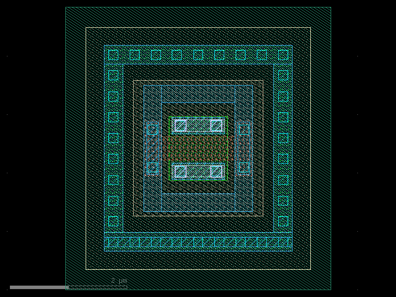
@gf.cell(schematic_function=rfpmos_hv_schematic, tags=["IHP", "mos", "hv", "rf"])
def rfpmos_hv(
    width: float = 1.0,
    length: float = 0.40,
    nf: int = 1,
    m: int = 1,
    cnt_rows: int = 1,
    met2_cont: bool = True,
    gat_ring: bool = True,
    guard_ring: str = "Yes",
    model: str = "sg13_hv_pmos",
) -> Component:
    """Create a high-voltage RF PMOS transistor.

    Args:
        width: Total width of the transistor in micrometers.
        length: Gate length in micrometers.
        nf: Number of fingers.
        m: Multiplier (number of parallel devices).
        cnt_rows: Number of contact rows.
        met2_cont: Include Metal2-to-contact connections.
        gat_ring: Include gate ring around the transistor.
        guard_ring: Guard ring type: "Yes", "No", "U", or "Top+Bottom".
        model: Device model name.

    Returns:
        Component with HV RF PMOS transistor layout.

    Raises:
        ValueError: If width, length, or nf is outside allowed range.
    """
    if width < TECH.rfpmos_hv_min_width or width > TECH.rfpmos_hv_max_width:
        raise ValueError(
            f"rfpmos_hv width={width} out of range [{TECH.rfpmos_hv_min_width}, {TECH.rfpmos_hv_max_width}]"
        )
    if length < TECH.rfpmos_hv_min_length or length > TECH.rfpmos_hv_max_length:
        raise ValueError(
            f"rfpmos_hv length={length} out of range [{TECH.rfpmos_hv_min_length}, {TECH.rfpmos_hv_max_length}]"
        )
    if nf < 1 or nf > TECH.rfpmos_hv_max_nf:
        raise ValueError(f"rfpmos_hv nf={nf} out of range [1, {TECH.rfpmos_hv_max_nf}]")

    c = _rf_mos_core(
        width,
        length,
        nf,
        cnt_rows,
        met2_cont,
        gat_ring,
        guard_ring,
        is_pmos=True,
        is_hv=True,
    )
    return c

rfpmos_hv

import warnings
warnings.filterwarnings("ignore", category=DeprecationWarning)

from ihp import PDK
from ihp import cells

PDK.activate()

c = cells.rfpmos_hv(width=1.0, length=0.4, nf=1, m=1, cnt_rows=1, met2_cont=True, gat_ring=True, guard_ring='Yes', model='sg13_hv_pmos').copy()
c.draw_ports()
c.plot()

rhigh

Create a vertical high-resistance polysilicon resistor (i.e. with dy as its length).

Parameters:

Name Type Description Default
dy float

length of the resistor in micrometers.

0.96
dx float

width of the resistor in micrometers.

0.5
resistance float | None

Target resistance in ohms (optional).

None
model str

Device model name.

'rhigh'
layer_poly tuple[int, int] | str | int | LayerEnum

Polysilicon layer.

'PolyResdrawing'
layer_heat tuple[int, int] | str | int | LayerEnum

Thermal resistor marker.

'HeatResdrawing'
layer_gate tuple[int, int] | str | int | LayerEnum

Gate polysilicon layer.

'GatPolydrawing'
layer_contact tuple[int, int] | str | int | LayerEnum

Contact layer.

'Contdrawing'
layer_metal1 tuple[int, int] | str | int | LayerEnum

Metal1 layer.

'Metal1drawing'
layer_metal1_pin tuple[int, int] | str | int | LayerEnum

Metal1 pin layer.

'Metal1pin'
layer_pSD tuple[int, int] | str | int | LayerEnum

PSD layer.

'pSDdrawing'
layer_nSD tuple[int, int] | str | int | LayerEnum

NSD layer

'nSDdrawing'
layer_block tuple[int, int] | str | int | LayerEnum

Blocking layer.

'EXTBlockdrawing'
layer_sal_block tuple[int, int] | str | int | LayerEnum

Salicide block layer.

'SalBlockdrawing'

Returns:

Type Description
Component

Component with high-resistance poly resistor layout.

Raises:

Type Description
ValueError

If dx (width) or dy (length) is outside allowed range.

Source code in ihp/cells/resistors.py
@gf.cell(schematic_function=rhigh_schematic, tags=["IHP", "resistor", "high-r"])
def rhigh(
    dy: float = 0.96,
    dx: float = 0.5,
    resistance: float | None = None,
    model: str = "rhigh",
    layer_poly: LayerSpec = "PolyResdrawing",
    layer_heat: LayerSpec = "HeatResdrawing",
    layer_gate: LayerSpec = "GatPolydrawing",
    layer_contact: LayerSpec = "Contdrawing",
    layer_metal1: LayerSpec = "Metal1drawing",
    layer_metal1_pin: LayerSpec = "Metal1pin",
    layer_pSD: LayerSpec = "pSDdrawing",
    layer_nSD: LayerSpec = "nSDdrawing",
    layer_block: LayerSpec = "EXTBlockdrawing",
    layer_sal_block: LayerSpec = "SalBlockdrawing",
) -> Component:
    """Create a vertical high-resistance polysilicon resistor (i.e. with dy as its length).

    Args:
        dy: length of the resistor in micrometers.
        dx: width of the resistor in micrometers.
        resistance: Target resistance in ohms (optional).
        model: Device model name.
        layer_poly: Polysilicon layer.
        layer_heat: Thermal resistor marker.
        layer_gate: Gate polysilicon layer.
        layer_contact: Contact layer.
        layer_metal1: Metal1 layer.
        layer_metal1_pin: Metal1 pin layer.
        layer_pSD: PSD layer.
        layer_nSD: NSD layer
        layer_block: Blocking layer.
        layer_sal_block: Salicide block layer.

    Returns:
        Component with high-resistance poly resistor layout.

    Raises:
        ValueError: If dx (width) or dy (length) is outside allowed range.
    """
    if dx < _TECH.rhigh_min_width or dx > _TECH.rhigh_max_width:
        raise ValueError(
            f"rhigh dx={dx} out of range [{_TECH.rhigh_min_width}, {_TECH.rhigh_max_width}]"
        )
    if dy < _TECH.rhigh_min_length or dy > _TECH.rhigh_max_length:
        raise ValueError(
            f"rhigh dy={dy} out of range [{_TECH.rhigh_min_length}, {_TECH.rhigh_max_length}]"
        )

    c = Component()

    # Constants
    RHIGH_MIN_DY = 0.4
    RHIGH_MIN_DX = 0.5
    GRID = 0.005

    SHEET_RESISTANCE = 300.0
    GAT_DY = 0.43

    # Fundamental geometry constants
    METAL_PAD_DY = 0.26
    METAL_CONTACT_MARGIN = 0.05
    GAT_METAL_MARGIN = 0.02

    BLOCK1_MARGIN = 0.18
    BLOCK2_MARGIN = 0.02

    # Snap to grid
    dy = max(dy, RHIGH_MIN_DY)
    dx = max(dx, RHIGH_MIN_DX)
    dy = round(dy / GRID) * GRID
    dx = round(dx / GRID) * GRID

    # Resistance calculation
    if resistance is None:
        n_squares = dy / dx
        resistance = n_squares * SHEET_RESISTANCE
    else:
        n_squares = dy / dx

    # Compute geometry
    body_origin = (0.0, 0.0)

    # Metal pad sizes
    metal_pad_dx = dx - 2 * GAT_METAL_MARGIN
    metal_pad_dy = METAL_PAD_DY

    # Metal pad positions
    metal_pad_left_x = GAT_METAL_MARGIN
    metal_pad_upper_y = dy + GAT_DY - metal_pad_dy - GAT_METAL_MARGIN
    metal_pad_lower_y = -GAT_DY + GAT_METAL_MARGIN

    # Contacts inside metal pads
    contact_dx = metal_pad_dx - 2 * METAL_CONTACT_MARGIN
    contact_dy = metal_pad_dy - 2 * METAL_CONTACT_MARGIN

    contact_left_x = metal_pad_left_x + METAL_CONTACT_MARGIN
    contact_upper_y = metal_pad_upper_y + METAL_CONTACT_MARGIN
    contact_lower_y = metal_pad_lower_y + METAL_CONTACT_MARGIN

    # Blocking layer geometry
    block1_dx = dx + 2 * BLOCK1_MARGIN
    block1_dy = dy + 2 * (GAT_DY + BLOCK1_MARGIN)
    block1_origin = ((dx - block1_dx) / 2, (dy - block1_dy) / 2)

    block2_dx = block1_dx + 2 * BLOCK2_MARGIN
    block2_dy = dy
    block2_origin = ((dx - block2_dx) / 2, (dy - block2_dy) / 2)

    # Draw resistor body (poly + heat)
    for ly in (layer_poly, layer_heat):
        add_rect(c, size=(dx, dy), layer=ly, origin=body_origin)

    # Gate extensions
    gate_size = (dx, GAT_DY)
    add_rect(c, gate_size, layer_gate, origin=(0.0, dy))
    add_rect(c, gate_size, layer_gate, origin=(0.0, -GAT_DY))

    # Contacts
    add_rect(
        c,
        (contact_dx, contact_dy),
        layer_contact,
        origin=(contact_left_x, contact_upper_y),
    )
    add_rect(
        c,
        (contact_dx, contact_dy),
        layer_contact,
        origin=(contact_left_x, contact_lower_y),
    )

    # Metal pads
    for ly in (layer_metal1_pin, layer_metal1):
        add_rect(
            c,
            (metal_pad_dx, metal_pad_dy),
            ly,
            origin=(metal_pad_left_x, metal_pad_upper_y),
        )
        add_rect(
            c,
            (metal_pad_dx, metal_pad_dy),
            ly,
            origin=(metal_pad_left_x, metal_pad_lower_y),
        )

    # Blocking 1
    for ly in (layer_block, layer_pSD, layer_nSD):
        add_rect(c, (block1_dx, block1_dy), ly, origin=block1_origin)

    # Blocking 2
    for ly in (layer_block, layer_sal_block):
        add_rect(c, (block2_dx, block2_dy), ly, origin=block2_origin)

    # Ports
    metal_pad_center_x = metal_pad_left_x + metal_pad_dx / 2.0
    metal_pad_upper_center_y = metal_pad_upper_y + metal_pad_dy / 2.0
    metal_pad_lower_center_y = metal_pad_lower_y + metal_pad_dy / 2.0

    c.add_port(
        name="P1",
        center=(metal_pad_center_x, metal_pad_upper_center_y),
        width=metal_pad_dx,
        orientation=90,
        layer=layer_metal1_pin,
        port_type="electrical",
    )

    c.add_port(
        name="P2",
        center=(metal_pad_center_x, metal_pad_lower_center_y),
        width=metal_pad_dx,
        orientation=270,
        layer=layer_metal1_pin,
        port_type="electrical",
    )

    # Metadata
    c.info.update(
        {
            "model": model,
            "dy": dy,
            "dx": dx,
            "resistance": resistance,
            "sheet_resistance": SHEET_RESISTANCE,
            "n_squares": n_squares,
        }
    )

    return c

rhigh

import warnings
warnings.filterwarnings("ignore", category=DeprecationWarning)

from ihp import PDK
from ihp import cells

PDK.activate()

c = cells.rhigh(dy=0.96, dx=0.5, model='rhigh', layer_poly='PolyResdrawing', layer_heat='HeatResdrawing', layer_gate='GatPolydrawing', layer_contact='Contdrawing', layer_metal1='Metal1drawing', layer_metal1_pin='Metal1pin', layer_pSD='pSDdrawing', layer_nSD='nSDdrawing', layer_block='EXTBlockdrawing', layer_sal_block='SalBlockdrawing').copy()
c.draw_ports()
c.plot()

rppd

Create a vertical P+ polysilicon resistor (i.e. with dy as its length).

Parameters:

Name Type Description Default
dy float

length of the resistor in micrometers.

0.5
dx float

width of the resistor in micrometers.

0.5
resistance float | None

Target resistance in ohms (optional).

None
model str

Device model name.

'rppd'
layer_poly tuple[int, int] | str | int | LayerEnum

Polysilicon layer.

'PolyResdrawing'
layer_heat tuple[int, int] | str | int | LayerEnum

Thermal resistor marker.

'HeatResdrawing'
layer_gate tuple[int, int] | str | int | LayerEnum

Gate polysilicon layer.

'GatPolydrawing'
layer_contact tuple[int, int] | str | int | LayerEnum

Contact layer.

'Contdrawing'
layer_metal1 tuple[int, int] | str | int | LayerEnum

Metal1 layer.

'Metal1drawing'
layer_metal1_pin tuple[int, int] | str | int | LayerEnum

Metal1 pin layer.

'Metal1pin'
layer_pSD tuple[int, int] | str | int | LayerEnum

PSD layer.

'pSDdrawing'
layer_block tuple[int, int] | str | int | LayerEnum

Blocking layer.

'EXTBlockdrawing'
layer_sal_block tuple[int, int] | str | int | LayerEnum

Salicide block layer.

'SalBlockdrawing'

Returns:

Type Description
Component

Component with P+ resistor layout.

Raises:

Type Description
ValueError

If dx (width) or dy (length) is outside allowed range.

Source code in ihp/cells/resistors.py
@gf.cell(schematic_function=rppd_schematic, tags=["IHP", "resistor", "unsilicided"])
def rppd(
    dy: float = 0.5,
    dx: float = 0.5,
    resistance: float | None = None,
    model: str = "rppd",
    layer_poly: LayerSpec = "PolyResdrawing",
    layer_heat: LayerSpec = "HeatResdrawing",
    layer_gate: LayerSpec = "GatPolydrawing",
    layer_contact: LayerSpec = "Contdrawing",
    layer_metal1: LayerSpec = "Metal1drawing",
    layer_metal1_pin: LayerSpec = "Metal1pin",
    layer_pSD: LayerSpec = "pSDdrawing",
    layer_block: LayerSpec = "EXTBlockdrawing",
    layer_sal_block: LayerSpec = "SalBlockdrawing",
) -> Component:
    """Create a vertical P+ polysilicon resistor (i.e. with dy as its length).

    Args:
        dy: length of the resistor in micrometers.
        dx: width of the resistor in micrometers.
        resistance: Target resistance in ohms (optional).
        model: Device model name.
        layer_poly: Polysilicon layer.
        layer_heat: Thermal resistor marker.
        layer_gate: Gate polysilicon layer.
        layer_contact: Contact layer.
        layer_metal1: Metal1 layer.
        layer_metal1_pin: Metal1 pin layer.
        layer_pSD: PSD layer.
        layer_block: Blocking layer.
        layer_sal_block: Salicide block layer.

    Returns:
        Component with P+ resistor layout.

    Raises:
        ValueError: If dx (width) or dy (length) is outside allowed range.
    """
    if dx < _TECH.rppd_min_width or dx > _TECH.rppd_max_width:
        raise ValueError(
            f"rppd dx={dx} out of range [{_TECH.rppd_min_width}, {_TECH.rppd_max_width}]"
        )
    if dy < _TECH.rppd_min_length or dy > _TECH.rppd_max_length:
        raise ValueError(
            f"rppd dy={dy} out of range [{_TECH.rppd_min_length}, {_TECH.rppd_max_length}]"
        )

    c = Component()

    # Constants
    RPPD_MIN_DY = 0.4
    RPPD_MIN_DX = 0.5
    GRID = 0.005

    SHEET_RESISTANCE = 300.0
    GAT_DY = 0.43

    # Geometry
    METAL_PAD_DY = 0.30
    METAL_CONTACT_MARGIN_DX = 0.05
    METAL_CONTACT_MARGIN_DY = 0.07
    GAT_METAL_MARGIN_DX = 0.02
    GAT_METAL_MARGIN_DY = 0.00

    BLOCK_MARGIN = 0.18
    BLOCK2_MARGIN = 0.02

    # Snap to grid
    dy = max(dy, RPPD_MIN_DY)
    dx = max(dx, RPPD_MIN_DX)
    dy = round(dy / GRID) * GRID
    dx = round(dx / GRID) * GRID

    # Resistance calculation
    if resistance is None:
        n_squares = dy / dx
        resistance = n_squares * SHEET_RESISTANCE
    else:
        n_squares = dy / dx

    # Geometry
    body_origin = (0.0, 0.0)

    # Metal pad sizes
    metal_pad_dx = dx - 2 * GAT_METAL_MARGIN_DX
    metal_pad_dy = METAL_PAD_DY

    # Metal pad coordinates
    metal_pad_left_x = GAT_METAL_MARGIN_DX
    metal_pad_upper_y = dy + GAT_DY - metal_pad_dy - GAT_METAL_MARGIN_DY
    metal_pad_lower_y = -GAT_DY + GAT_METAL_MARGIN_DY

    # Contact sizes
    contact_dx = metal_pad_dx - 2 * METAL_CONTACT_MARGIN_DX
    contact_dy = metal_pad_dy - 2 * METAL_CONTACT_MARGIN_DY

    contact_left_x = metal_pad_left_x + METAL_CONTACT_MARGIN_DX
    contact_upper_y = metal_pad_upper_y + METAL_CONTACT_MARGIN_DY
    contact_lower_y = metal_pad_lower_y + METAL_CONTACT_MARGIN_DY

    # Blocking layers
    block_dx = dx + 2 * BLOCK_MARGIN
    block_dy = dy + 2 * (GAT_DY + BLOCK_MARGIN)
    block_origin = ((dx - block_dx) / 2.0, (dy - block_dy) / 2.0)

    block2_dx = block_dx + 2 * BLOCK2_MARGIN
    block2_dy = dy
    block2_origin = ((dx - block2_dx) / 2.0, (dy - block2_dy) / 2.0)

    # Draw resistor body
    for ly in (layer_poly, layer_heat):
        add_rect(c, size=(dx, dy), layer=ly, origin=body_origin)

    # Gate poly extensions
    gate_size = (dx, GAT_DY)
    add_rect(c, size=gate_size, layer=layer_gate, origin=(0.0, dy))
    add_rect(c, size=gate_size, layer=layer_gate, origin=(0.0, -GAT_DY))

    # Contacts
    add_rect(
        c,
        size=(contact_dx, contact_dy),
        layer=layer_contact,
        origin=(contact_left_x, contact_upper_y),
    )
    add_rect(
        c,
        size=(contact_dx, contact_dy),
        layer=layer_contact,
        origin=(contact_left_x, contact_lower_y),
    )

    # Metal pads (pin + metal1)
    for ly in (layer_metal1_pin, layer_metal1):
        add_rect(
            c,
            size=(metal_pad_dx, metal_pad_dy),
            layer=ly,
            origin=(metal_pad_left_x, metal_pad_upper_y),
        )
        add_rect(
            c,
            size=(metal_pad_dx, metal_pad_dy),
            layer=ly,
            origin=(metal_pad_left_x, metal_pad_lower_y),
        )

    # Blocking layers
    for ly in (layer_block, layer_pSD):
        add_rect(c, size=(block_dx, block_dy), layer=ly, origin=block_origin)

    for ly in (layer_block, layer_sal_block):
        add_rect(c, size=(block2_dx, block2_dy), layer=ly, origin=block2_origin)

    # Ports
    metal_pad_center_x = metal_pad_left_x + metal_pad_dx / 2.0
    metal_pad_upper_center_y = metal_pad_upper_y + metal_pad_dy / 2.0
    metal_pad_lower_center_y = metal_pad_lower_y + metal_pad_dy / 2.0

    c.add_port(
        name="P1",
        center=(metal_pad_center_x, metal_pad_upper_center_y),
        width=metal_pad_dx,
        orientation=90,
        layer=layer_metal1_pin,
        port_type="electrical",
    )

    c.add_port(
        name="P2",
        center=(metal_pad_center_x, metal_pad_lower_center_y),
        width=metal_pad_dx,
        orientation=270,
        layer=layer_metal1_pin,
        port_type="electrical",
    )

    # Metadata
    c.info.update(
        {
            "model": model,
            "dy": dy,
            "dx": dx,
            "resistance": resistance,
            "sheet_resistance": SHEET_RESISTANCE,
            "n_squares": n_squares,
        }
    )

    return c

rppd

import warnings
warnings.filterwarnings("ignore", category=DeprecationWarning)

from ihp import PDK
from ihp import cells

PDK.activate()

c = cells.rppd(dy=0.5, dx=0.5, model='rppd', layer_poly='PolyResdrawing', layer_heat='HeatResdrawing', layer_gate='GatPolydrawing', layer_contact='Contdrawing', layer_metal1='Metal1drawing', layer_metal1_pin='Metal1pin', layer_pSD='pSDdrawing', layer_block='EXTBlockdrawing', layer_sal_block='SalBlockdrawing').copy()
c.draw_ports()
c.plot()

rsil

Create a vertical silicided polysilicon resistor (i.e. with dy as its length)

Parameters:

Name Type Description Default
dy float

length of the resistor in micrometers.

0.5
dx float

width of the resistor in micrometers.

0.5
resistance float | None

Target resistance in ohms (optional).

None
model str

Device model name.

'rsil'
layer_poly tuple[int, int] | str | int | LayerEnum

Polysilicon layer.

'PolyResdrawing'
layer_heat tuple[int, int] | str | int | LayerEnum

Thermal resistor marker.

'HeatResdrawing'
layer_gate tuple[int, int] | str | int | LayerEnum

Gate polysilicon layer.

'GatPolydrawing'
layer_contact tuple[int, int] | str | int | LayerEnum

Contact layer.

'Contdrawing'
layer_metal1 tuple[int, int] | str | int | LayerEnum

Metal1 layer.

'Metal1drawing'
layer_metal1_pin tuple[int, int] | str | int | LayerEnum

Metal1 pin layer.

'Metal1pin'
layer_res_mark tuple[int, int] | str | int | LayerEnum

Resistor marker layer.

'RESdrawing'
layer_block tuple[int, int] | str | int | LayerEnum

Blocking layer.

'EXTBlockdrawing'

Returns:

Type Description
Component

Component with silicided poly resistor layout.

Raises:

Type Description
ValueError

If dx (width) or dy (length) is outside allowed range.

Source code in ihp/cells/resistors.py
@gf.cell(schematic_function=rsil_schematic, tags=["IHP", "resistor", "silicided"])
def rsil(
    dy: float = 0.5,
    dx: float = 0.5,
    resistance: float | None = None,
    model: str = "rsil",
    layer_poly: LayerSpec = "PolyResdrawing",
    layer_heat: LayerSpec = "HeatResdrawing",
    layer_gate: LayerSpec = "GatPolydrawing",
    layer_contact: LayerSpec = "Contdrawing",
    layer_metal1: LayerSpec = "Metal1drawing",
    layer_metal1_pin: LayerSpec = "Metal1pin",
    layer_res_mark: LayerSpec = "RESdrawing",
    layer_block: LayerSpec = "EXTBlockdrawing",
) -> Component:
    """Create a vertical silicided polysilicon resistor (i.e. with dy as its length)

    Args:
        dy: length of the resistor in micrometers.
        dx: width of the resistor in micrometers.
        resistance: Target resistance in ohms (optional).
        model: Device model name.
        layer_poly: Polysilicon layer.
        layer_heat: Thermal resistor marker.
        layer_gate: Gate polysilicon layer.
        layer_contact: Contact layer.
        layer_metal1: Metal1 layer.
        layer_metal1_pin: Metal1 pin layer.
        layer_res_mark: Resistor marker layer.
        layer_block: Blocking layer.

    Returns:
        Component with silicided poly resistor layout.

    Raises:
        ValueError: If dx (width) or dy (length) is outside allowed range.
    """
    if dx < _TECH.rsil_min_width or dx > _TECH.rsil_max_width:
        raise ValueError(
            f"rsil dx={dx} out of range [{_TECH.rsil_min_width}, {_TECH.rsil_max_width}]"
        )
    if dy < _TECH.rsil_min_length or dy > _TECH.rsil_max_length:
        raise ValueError(
            f"rsil dy={dy} out of range [{_TECH.rsil_min_length}, {_TECH.rsil_max_length}]"
        )

    c = Component()

    # Constants
    RSIL_MIN_DY = 0.4
    RSIL_MIN_DX = 0.4
    GRID = 0.005

    SHEET_RESISTANCE = 7.0
    GAT_DY = 0.35

    # Geometry
    METAL_PAD_DY = 0.26
    GAT_METAL_MARGIN = 0.02
    METAL_CONTACT_MARGIN = 0.05
    BLOCK_MARGIN = 0.18

    # Snap to grid
    dy = max(dy, RSIL_MIN_DY)
    dx = max(dx, RSIL_MIN_DX)
    dy = round(dy / GRID) * GRID
    dx = round(dx / GRID) * GRID

    # Resistance calculation
    if resistance is None:
        n_squares = dy / dx
        resistance = n_squares * SHEET_RESISTANCE
    else:
        n_squares = dy / dx

    # Compute geometry
    # Resistor body bottom-left at (0,0)
    body_origin = (0.0, 0.0)

    # Pad sizes
    metal_pad_dx = dx - 2 * GAT_METAL_MARGIN
    metal_pad_dy = METAL_PAD_DY

    # Pad coordinates
    metal_pad_left_x = GAT_METAL_MARGIN
    metal_pad_upper_y = dy + GAT_DY - metal_pad_dy - GAT_METAL_MARGIN
    metal_pad_lower_y = -GAT_DY + GAT_METAL_MARGIN

    # Contacts inside pads
    contact_dx = metal_pad_dx - 2 * METAL_CONTACT_MARGIN
    contact_dy = metal_pad_dy - 2 * METAL_CONTACT_MARGIN
    contact_x = metal_pad_left_x + METAL_CONTACT_MARGIN
    contact_upper_y = metal_pad_upper_y + METAL_CONTACT_MARGIN
    contact_lower_y = metal_pad_lower_y + METAL_CONTACT_MARGIN

    # blocking rectangle size & origin
    block_dx = dx + 2 * BLOCK_MARGIN
    block_dy = dy + 2 * (GAT_DY + BLOCK_MARGIN)
    block_origin = ((dx - block_dx) / 2.0, (dy - block_dy) / 2.0)

    # Draw resistor body (polysilicon + heat + res marker)
    for ly in (layer_poly, layer_heat, layer_res_mark):
        add_rect(c, size=(dx, dy), layer=ly, origin=body_origin)

    # Gate extensions (top and bottom)
    gate_size = (dx, GAT_DY)
    add_rect(c, size=gate_size, layer=layer_gate, origin=(0.0, dy))
    add_rect(c, size=gate_size, layer=layer_gate, origin=(0.0, -GAT_DY))

    # Metal pads (pin then metal1)
    for ly in (layer_metal1_pin, layer_metal1):
        add_rect(
            c,
            size=(metal_pad_dx, metal_pad_dy),
            layer=ly,
            origin=(metal_pad_left_x, metal_pad_upper_y),
        )
        add_rect(
            c,
            size=(metal_pad_dx, metal_pad_dy),
            layer=ly,
            origin=(metal_pad_left_x, metal_pad_lower_y),
        )

    # Contacts (inside metal pads)
    add_rect(
        c,
        size=(contact_dx, contact_dy),
        layer=layer_contact,
        origin=(contact_x, contact_upper_y),
    )
    add_rect(
        c,
        size=(contact_dx, contact_dy),
        layer=layer_contact,
        origin=(contact_x, contact_lower_y),
    )

    # Blocking layer
    add_rect(c, size=(block_dx, block_dy), layer=layer_block, origin=block_origin)

    # Ports (derive from pad geometry)
    pad_center_x = metal_pad_left_x + metal_pad_dx / 2.0
    pad_upper_center_y = metal_pad_upper_y + metal_pad_dy / 2.0
    pad_lower_center_y = metal_pad_lower_y + metal_pad_dy / 2.0

    c.add_port(
        name="P1",
        center=(pad_center_x, pad_upper_center_y),
        width=metal_pad_dx,
        orientation=90,
        layer=layer_metal1_pin,
        port_type="electrical",
    )

    c.add_port(
        name="P2",
        center=(pad_center_x, pad_lower_center_y),
        width=metal_pad_dx,
        orientation=270,
        layer=layer_metal1_pin,
        port_type="electrical",
    )

    # Metadata
    c.info.update(
        {
            "model": model,
            "dy": dy,
            "dx": dx,
            "resistance": resistance,
            "sheet_resistance": SHEET_RESISTANCE,
            "n_squares": n_squares,
        }
    )

    return c

rsil

import warnings
warnings.filterwarnings("ignore", category=DeprecationWarning)

from ihp import PDK
from ihp import cells

PDK.activate()

c = cells.rsil(dy=0.5, dx=0.5, model='rsil', layer_poly='PolyResdrawing', layer_heat='HeatResdrawing', layer_gate='GatPolydrawing', layer_contact='Contdrawing', layer_metal1='Metal1drawing', layer_metal1_pin='Metal1pin', layer_res_mark='RESdrawing', layer_block='EXTBlockdrawing').copy()
c.draw_ports()
c.plot()

sealring

Create a seal ring for die protection.

Parameters:

Name Type Description Default
width float

Inner width of the seal ring in micrometers.

200.0
height float

Inner height of the seal ring in micrometers.

200.0
ring_width float

Width of the seal ring metal in micrometers.

5.0
layer_metal1 tuple[int, int] | str | int | LayerEnum

Metal1 layer.

'Metal1drawing'
layer_metal2 tuple[int, int] | str | int | LayerEnum

Metal2 layer.

'Metal2drawing'
layer_metal3 tuple[int, int] | str | int | LayerEnum

Metal3 layer.

'Metal3drawing'
layer_metal4 tuple[int, int] | str | int | LayerEnum

Metal4 layer.

'Metal4drawing'
layer_metal5 tuple[int, int] | str | int | LayerEnum

Metal5 layer.

'Metal5drawing'
layer_topmetal1 tuple[int, int] | str | int | LayerEnum

TopMetal1 layer.

'TopMetal1drawing'
layer_topmetal2 tuple[int, int] | str | int | LayerEnum

TopMetal2 layer.

'TopMetal2drawing'
layer_via1 tuple[int, int] | str | int | LayerEnum

Via1 layer.

'Via1drawing'
layer_via2 tuple[int, int] | str | int | LayerEnum

Via2 layer.

'Via2drawing'
layer_via3 tuple[int, int] | str | int | LayerEnum

Via3 layer.

'Via3drawing'
layer_via4 tuple[int, int] | str | int | LayerEnum

Via4 layer.

'Via4drawing'
layer_topvia1 tuple[int, int] | str | int | LayerEnum

TopVia1 layer.

'TopVia1drawing'
layer_topvia2 tuple[int, int] | str | int | LayerEnum

TopVia2 layer.

'TopVia2drawing'
layer_sealring tuple[int, int] | str | int | LayerEnum

Seal ring marker layer.

'EdgeSealdrawing'

Returns:

Type Description
Component

Component with seal ring layout.

Raises:

Type Description
ValueError

If width or height is outside allowed range.

Source code in ihp/cells/passives.py
@gf.cell(tags=["IHP", "sealring"])
def sealring(
    width: float = 200.0,
    height: float = 200.0,
    ring_width: float = 5.0,
    layer_metal1: LayerSpec = "Metal1drawing",
    layer_metal2: LayerSpec = "Metal2drawing",
    layer_metal3: LayerSpec = "Metal3drawing",
    layer_metal4: LayerSpec = "Metal4drawing",
    layer_metal5: LayerSpec = "Metal5drawing",
    layer_topmetal1: LayerSpec = "TopMetal1drawing",
    layer_topmetal2: LayerSpec = "TopMetal2drawing",
    layer_via1: LayerSpec = "Via1drawing",
    layer_via2: LayerSpec = "Via2drawing",
    layer_via3: LayerSpec = "Via3drawing",
    layer_via4: LayerSpec = "Via4drawing",
    layer_topvia1: LayerSpec = "TopVia1drawing",
    layer_topvia2: LayerSpec = "TopVia2drawing",
    layer_sealring: LayerSpec = "EdgeSealdrawing",
) -> Component:
    """Create a seal ring for die protection.

    Args:
        width: Inner width of the seal ring in micrometers.
        height: Inner height of the seal ring in micrometers.
        ring_width: Width of the seal ring metal in micrometers.
        layer_metal1: Metal1 layer.
        layer_metal2: Metal2 layer.
        layer_metal3: Metal3 layer.
        layer_metal4: Metal4 layer.
        layer_metal5: Metal5 layer.
        layer_topmetal1: TopMetal1 layer.
        layer_topmetal2: TopMetal2 layer.
        layer_via1: Via1 layer.
        layer_via2: Via2 layer.
        layer_via3: Via3 layer.
        layer_via4: Via4 layer.
        layer_topvia1: TopVia1 layer.
        layer_topvia2: TopVia2 layer.
        layer_sealring: Seal ring marker layer.

    Returns:
        Component with seal ring layout.

    Raises:
        ValueError: If width or height is outside allowed range.
    """
    if width < tech.TECH.sealring_min_width or width > tech.TECH.sealring_max_width:
        raise ValueError(
            f"sealring width={width} out of range [{tech.TECH.sealring_min_width}, {tech.TECH.sealring_max_width}]"
        )
    if height < tech.TECH.sealring_min_height or height > tech.TECH.sealring_max_height:
        raise ValueError(
            f"sealring height={height} out of range [{tech.TECH.sealring_min_height}, {tech.TECH.sealring_max_height}]"
        )

    c = Component()

    # Create seal ring on all metal layers
    metal_layers = [
        layer_metal1,
        layer_metal2,
        layer_metal3,
        layer_metal4,
        layer_metal5,
        layer_topmetal1,
        layer_topmetal2,
    ]

    # Create ring on each metal layer
    for metal_layer in metal_layers:
        # Outer rectangle
        outer = gf.components.rectangle(
            size=(width + 2 * ring_width, height + 2 * ring_width),
            layer=metal_layer,
            centered=True,
        )

        # Inner rectangle (to create ring)
        inner = gf.components.rectangle(
            size=(width, height),
            layer=metal_layer,
            centered=True,
        )

        # Create ring by boolean subtraction
        ring = gf.boolean(outer, inner, "A-B", layer=metal_layer)
        c.add_ref(ring)

    # Add vias between metal layers
    via_layers = [
        layer_via1,
        layer_via2,
        layer_via3,
        layer_via4,
        layer_topvia1,
        layer_topvia2,
    ]

    # Via arrays in the ring
    via_size = 0.26
    via_spacing = 0.36

    for via_layer in via_layers:
        # Calculate number of vias along each edge
        n_vias_x = int((width + ring_width - via_size) / via_spacing)
        n_vias_y = int((height + ring_width - via_size) / via_spacing)

        # Top edge vias
        for i in range(n_vias_x):
            x = -width / 2 - ring_width / 2 + via_size / 2 + i * via_spacing
            y = height / 2 + ring_width / 2

            via = gf.components.rectangle(
                size=(via_size, via_size),
                layer=via_layer,
                centered=True,
            )
            via_ref = c.add_ref(via)
            via_ref.move((x, y))

        # Bottom edge vias
        for i in range(n_vias_x):
            x = -width / 2 - ring_width / 2 + via_size / 2 + i * via_spacing
            y = -height / 2 - ring_width / 2

            via = gf.components.rectangle(
                size=(via_size, via_size),
                layer=via_layer,
                centered=True,
            )
            via_ref = c.add_ref(via)
            via_ref.move((x, y))

        # Left edge vias
        for i in range(n_vias_y):
            x = -width / 2 - ring_width / 2
            y = -height / 2 - ring_width / 2 + via_size / 2 + i * via_spacing

            via = gf.components.rectangle(
                size=(via_size, via_size),
                layer=via_layer,
                centered=True,
            )
            via_ref = c.add_ref(via)
            via_ref.move((x, y))

        # Right edge vias
        for i in range(n_vias_y):
            x = width / 2 + ring_width / 2
            y = -height / 2 - ring_width / 2 + via_size / 2 + i * via_spacing

            via = gf.components.rectangle(
                size=(via_size, via_size),
                layer=via_layer,
                centered=True,
            )
            via_ref = c.add_ref(via)
            via_ref.move((x, y))

    # Seal ring marker
    seal_mark = gf.components.rectangle(
        size=(width + 2 * ring_width + 1.0, height + 2 * ring_width + 1.0),
        layer=layer_sealring,
        centered=True,
    )
    seal_inner = gf.components.rectangle(
        size=(width - 1.0, height - 1.0),
        layer=layer_sealring,
        centered=True,
    )
    seal_ring_mark = gf.boolean(seal_mark, seal_inner, "A-B", layer=layer_sealring)
    c.add_ref(seal_ring_mark)

    # Add metadata
    c.info["type"] = "sealring"
    c.info["width"] = width
    c.info["height"] = height
    c.info["ring_width"] = ring_width

    return c

sealring

import warnings
warnings.filterwarnings("ignore", category=DeprecationWarning)

from ihp import PDK
from ihp import cells

PDK.activate()

c = cells.sealring(width=200.0, height=200.0, ring_width=5.0, layer_metal1='Metal1drawing', layer_metal2='Metal2drawing', layer_metal3='Metal3drawing', layer_metal4='Metal4drawing', layer_metal5='Metal5drawing', layer_topmetal1='TopMetal1drawing', layer_topmetal2='TopMetal2drawing', layer_via1='Via1drawing', layer_via2='Via2drawing', layer_via3='Via3drawing', layer_via4='Via4drawing', layer_topvia1='TopVia1drawing', layer_topvia2='TopVia2drawing', layer_sealring='EdgeSealdrawing').copy()
c.draw_ports()
c.plot()

straight

Returns a Straight waveguide.

Parameters:

Name Type Description Default
length float

straight length (um).

10
cross_section CrossSection | str | dict[str, Any] | Callable[..., CrossSection] | SymmetricalCrossSection | DCrossSection

specification (CrossSection, string or dict).

'strip'
width float | None

width of the waveguide. If None, it will use the width of the cross_section.

None
npoints int

number of points.

2
Source code in ihp/cells/waveguides.py
@gf.cell(tags=["IHP", "waveguide", "straight"])
def straight(
    length: float = 10,
    cross_section: CrossSectionSpec = "strip",
    width: float | None = None,
    npoints: int = 2,
) -> gf.Component:
    """Returns a Straight waveguide.

    Args:
        length: straight length (um).
        cross_section: specification (CrossSection, string or dict).
        width: width of the waveguide. If None, it will use the width of the cross_section.
        npoints: number of points.
    """
    return gf.c.straight(
        length=length, cross_section=cross_section, width=width, npoints=npoints
    )

straight

import warnings
warnings.filterwarnings("ignore", category=DeprecationWarning)

from ihp import PDK
from ihp import cells

PDK.activate()

c = cells.straight(length=10, cross_section='strip', npoints=2).copy()
c.draw_ports()
c.plot()

straight_metal

Returns a Straight waveguide.

Parameters:

Name Type Description Default
length float

straight length (um).

10
cross_section CrossSection | str | dict[str, Any] | Callable[..., CrossSection] | SymmetricalCrossSection | DCrossSection

specification (CrossSection, string or dict).

'metal_routing'
width float | None

width of the waveguide. If None, it will use the width of the cross_section.

None
Source code in ihp/cells/waveguides.py
@gf.cell(tags=["IHP", "wire", "straight"])
def straight_metal(
    length: float = 10,
    cross_section: CrossSectionSpec = "metal_routing",
    width: float | None = None,
) -> gf.Component:
    """Returns a Straight waveguide.

    Args:
        length: straight length (um).
        cross_section: specification (CrossSection, string or dict).
        width: width of the waveguide. If None, it will use the width of the cross_section.
    """
    return gf.c.straight(
        length=length, cross_section=cross_section, width=width, npoints=2
    )

straight_metal

import warnings
warnings.filterwarnings("ignore", category=DeprecationWarning)

from ihp import PDK
from ihp import cells

PDK.activate()

c = cells.straight_metal(length=10, cross_section='metal_routing').copy()
c.draw_ports()
c.plot()

svaricap

Create a MOS varicap (variable capacitor).

Parameters:

Name Type Description Default
width float

Width of the varicap in micrometers.

1.0
length float

Length of the varicap in micrometers.

1.0
nf int

Number of fingers.

1
model str

Device model name.

'sg13_hv_svaricap'
layer_nwell tuple[int, int] | str | int | LayerEnum

N-well layer.

'NWelldrawing'
layer_activ tuple[int, int] | str | int | LayerEnum

Active region layer.

'Activdrawing'
layer_gatpoly tuple[int, int] | str | int | LayerEnum

Gate polysilicon layer.

'GatPolydrawing'
layer_nsd tuple[int, int] | str | int | LayerEnum

N+ source/drain doping layer.

'nSDdrawing'
layer_cont tuple[int, int] | str | int | LayerEnum

Contact layer.

'Contdrawing'
layer_metal1 tuple[int, int] | str | int | LayerEnum

Metal1 layer.

'Metal1drawing'
layer_varicap tuple[int, int] | str | int | LayerEnum

Varicap marker layer.

'Varicapdrawing'

Returns:

Type Description
Component

Component with varicap layout.

Source code in ihp/cells/passives.py
@gf.cell(schematic_function=svaricap_schematic, tags=["IHP", "varicap", "hv"])
def svaricap(
    width: float = 1.0,
    length: float = 1.0,
    nf: int = 1,
    model: str = "sg13_hv_svaricap",
    layer_nwell: LayerSpec = "NWelldrawing",
    layer_activ: LayerSpec = "Activdrawing",
    layer_gatpoly: LayerSpec = "GatPolydrawing",
    layer_nsd: LayerSpec = "nSDdrawing",
    layer_cont: LayerSpec = "Contdrawing",
    layer_metal1: LayerSpec = "Metal1drawing",
    layer_metal1_pin: LayerSpec = "Metal1pin",
    layer_varicap: LayerSpec = "Varicapdrawing",
) -> Component:
    """Create a MOS varicap (variable capacitor).

    Args:
        width: Width of the varicap in micrometers.
        length: Length of the varicap in micrometers.
        nf: Number of fingers.
        model: Device model name.
        layer_nwell: N-well layer.
        layer_activ: Active region layer.
        layer_gatpoly: Gate polysilicon layer.
        layer_nsd: N+ source/drain doping layer.
        layer_cont: Contact layer.
        layer_metal1: Metal1 layer.
        layer_varicap: Varicap marker layer.

    Returns:
        Component with varicap layout.
    """
    c = Component()

    # Design rules
    var_min_width = 0.5
    var_min_length = 0.5
    gate_ext = 0.18
    active_ext = 0.23
    cont_size = 0.16
    cont_enc = 0.07
    nwell_enc = 0.31

    # Validate dimensions
    width = max(width, var_min_width)
    length = max(length, var_min_length)

    # Grid snap
    grid = 0.005
    width = round(width / grid) * grid
    length = round(length / grid) * grid

    # Calculate finger dimensions
    finger_width = width / nf
    finger_pitch = finger_width + 0.5

    # N-Well
    nwell = gf.components.rectangle(
        size=(
            length + 2 * active_ext + 2 * nwell_enc,
            nf * finger_pitch + 2 * nwell_enc,
        ),
        layer=layer_nwell,
        centered=True,
    )
    c.add_ref(nwell)

    # Create varicap fingers
    for i in range(nf):
        y_offset = (i - nf / 2 + 0.5) * finger_pitch

        # Gate poly (acts as one terminal)
        gate = gf.components.rectangle(
            size=(length, finger_width + 2 * gate_ext),
            layer=layer_gatpoly,
        )
        gate_ref = c.add_ref(gate)
        gate_ref.move((-length / 2, y_offset - finger_width / 2 - gate_ext))

        # Active region (acts as other terminal)
        active = gf.components.rectangle(
            size=(length + 2 * active_ext, finger_width),
            layer=layer_activ,
        )
        active_ref = c.add_ref(active)
        active_ref.move((-length / 2 - active_ext, y_offset - finger_width / 2))

        # N+ implant for active region
        nsd = gf.components.rectangle(
            size=(length + 2 * active_ext, finger_width),
            layer=layer_nsd,
        )
        nsd_ref = c.add_ref(nsd)
        nsd_ref.move((-length / 2 - active_ext, y_offset - finger_width / 2))

        # Contacts on active regions (source/drain)
        # Left side contacts
        cont_left = gf.components.rectangle(
            size=(cont_size, cont_size),
            layer=layer_cont,
        )
        cont_left_ref = c.add_ref(cont_left)
        cont_left_ref.move(
            (-length / 2 - active_ext + cont_enc, y_offset - cont_size / 2)
        )

        # Right side contacts
        cont_right = gf.components.rectangle(
            size=(cont_size, cont_size),
            layer=layer_cont,
        )
        cont_right_ref = c.add_ref(cont_right)
        cont_right_ref.move(
            (length / 2 + active_ext - cont_enc - cont_size, y_offset - cont_size / 2)
        )

    # Metal connections
    # Gate connection (Metal1)
    gate_metal = gf.components.rectangle(
        size=(1.0, nf * finger_pitch),
        layer=layer_metal1,
    )
    gate_metal_ref = c.add_ref(gate_metal)
    gate_metal_ref.move((-length / 2 - 1.5, -nf * finger_pitch / 2))

    # Active connection (Metal1)
    active_metal = gf.components.rectangle(
        size=(1.0, nf * finger_pitch),
        layer=layer_metal1,
    )
    active_metal_ref = c.add_ref(active_metal)
    active_metal_ref.move((length / 2 + 0.5, -nf * finger_pitch / 2))

    # Varicap marker
    var_mark = gf.components.rectangle(
        size=(length + 2 * active_ext + 0.5, nf * finger_pitch + 0.5),
        layer=layer_varicap,
        centered=True,
    )
    c.add_ref(var_mark)

    # Add ports
    c.add_port(
        name="G",
        center=(-length / 2 - 1.0, 0),
        width=nf * finger_pitch,
        orientation=180,
        layer=layer_metal1_pin,
        port_type="electrical",
    )

    c.add_port(
        name="B",
        center=(length / 2 + 1.0, 0),
        width=nf * finger_pitch,
        orientation=0,
        layer=layer_metal1_pin,
        port_type="electrical",
    )

    return c

svaricap

import warnings
warnings.filterwarnings("ignore", category=DeprecationWarning)

from ihp import PDK
from ihp import cells

PDK.activate()

c = cells.svaricap(width=1.0, length=1.0, nf=1, model='sg13_hv_svaricap', layer_nwell='NWelldrawing', layer_activ='Activdrawing', layer_gatpoly='GatPolydrawing', layer_nsd='nSDdrawing', layer_cont='Contdrawing', layer_metal1='Metal1drawing', layer_metal1_pin='Metal1pin', layer_varicap='Varicapdrawing').copy()
c.draw_ports()
c.plot()

text_rectangular

Pixel based font, guaranteed to be manhattan, without acute angles.

Parameters:

Name Type Description Default
text str

string.

'abc'
size float

pixel size.

3
justify str

left, right or center.

'left'
layer tuple[int, int] | str | int | LayerEnum

for text.

'TopMetal2drawing'
Source code in ihp/cells/text.py
@gf.cell(tags=["IHP", "text"])
def text_rectangular(
    text: str = "abc",
    size: float = 3,
    justify: str = "left",
    layer: LayerSpec = "TopMetal2drawing",
) -> gf.Component:
    """Pixel based font, guaranteed to be manhattan, without acute angles.

    Args:
        text: string.
        size: pixel size.
        justify: left, right or center.
        layer: for text.
    """
    return gf.c.text_rectangular(
        text=text, size=size, justify=justify, position=(0.0, 0.0), layer=layer
    )

text_rectangular

import warnings
warnings.filterwarnings("ignore", category=DeprecationWarning)

from ihp import PDK
from ihp import cells

PDK.activate()

c = cells.text_rectangular(text='abc', size=3, justify='left', layer='TopMetal2drawing').copy()
c.draw_ports()
c.plot()

text_rectangular_multi_layer

Returns rectangular text in different layers.

Parameters:

Name Type Description Default
text str

string of text.

'abc'
layers Sequence[tuple[int, int] | str | int | LayerEnum]

list of layers to replicate the text.

('TopMetal2drawing',)
text_factory str | Callable[..., Component] | dict[str, Any] | DKCell | partial[Component]

function to create the text Components.

'text_rectangular'
kwargs Any

keyword arguments for text_factory.

required
Source code in ihp/cells/text.py
@gf.cell(tags=["IHP", "text"])
def text_rectangular_multi_layer(
    text: str = "abc",
    layers: LayerSpecs = ("TopMetal2drawing",),
    text_factory: ComponentSpec = "text_rectangular",
    **kwargs: Any,
) -> gf.Component:
    """Returns rectangular text in different layers.

    Args:
        text: string of text.
        layers: list of layers to replicate the text.
        text_factory: function to create the text Components.
        kwargs: keyword arguments for text_factory.
    """
    return gf.c.text_rectangular_multi_layer(
        text=text,
        layers=layers,
        text_factory=text_factory,
        **kwargs,
    )

text_rectangular_multi_layer

import warnings
warnings.filterwarnings("ignore", category=DeprecationWarning)

from ihp import PDK
from ihp import cells

PDK.activate()

c = cells.text_rectangular_multi_layer(text='abc', layers=('TopMetal2drawing',), text_factory='text_rectangular').copy()
c.draw_ports()
c.plot()

tline

Return a straight coplanar transmission line.

Creates a signal straight and a wider ground straight aligned around it. The ground plane extends 3x the signal width beyond each end of the signal line and is 7x as wide. When two ground cross-sections are provided the component produces a stripline (ground above and below).

Parameters:

Name Type Description Default
length float

Length of the signal line (um).

10
signal_cross_section CrossSection | str | dict[str, Any] | Callable[..., CrossSection] | SymmetricalCrossSection | DCrossSection

Cross-section for the signal line.

'topmetal2_routing'
ground_cross_section CrossSection | str | dict[str, Any] | Callable[..., CrossSection] | SymmetricalCrossSection | DCrossSection | list[CrossSection | str | dict[str, Any] | Callable[..., CrossSection] | SymmetricalCrossSection | DCrossSection]

Cross-section for the ground line. Accepts a single spec for microstrip or a two-element list [lower, upper] for stripline.

'topmetal1_routing'
width float | None

Signal line width (um). Mutually exclusive with Z0.

None
Z0 float | None

Target characteristic impedance (ohms). Mutually exclusive with width.

None
npoints int

Number of points used to draw the straights.

2

Returns:

Type Description
Component

A Component containing signal and ground lines.

Raises:

Type Description
ValueError

If both width and Z0 are provided.

Source code in ihp/cells/waveguides.py
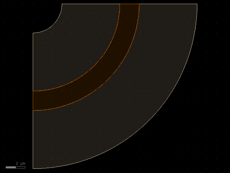
@gf.cell
def tline(
    length: float = 10,
    signal_cross_section: CrossSectionSpec = "topmetal2_routing",
    ground_cross_section: CrossSectionSpec
    | list[CrossSectionSpec] = "topmetal1_routing",
    width: float | None = None,
    Z0: float | None = None,
    npoints: int = 2,
) -> gf.Component:
    """Return a straight coplanar transmission line.

    Creates a signal straight and a wider ground straight aligned around it.
    The ground plane extends 3x the signal width beyond each end of the
    signal line and is 7x as wide.  When two ground cross-sections are
    provided the component produces a stripline (ground above and below).

    Args:
        length: Length of the signal line (um).
        signal_cross_section: Cross-section for the signal line.
        ground_cross_section: Cross-section for the ground line.
            Accepts a single spec for microstrip or a two-element list
            ``[lower, upper]`` for stripline.
        width: Signal line width (um). Mutually exclusive with Z0.
        Z0: Target characteristic impedance (ohms). Mutually exclusive
            with width.
        npoints: Number of points used to draw the straights.

    Returns:
        A Component containing signal and ground lines.

    Raises:
        ValueError: If both *width* and *Z0* are provided.
    """
    width, Z0 = _resolve_tline_width_and_Z0(
        width=width,
        Z0=Z0,
        signal_cross_section=signal_cross_section,
        ground_cross_section=ground_cross_section,
    )

    c = gf.Component()

    signal = c.add_ref(
        gf.c.straight(
            length=length,
            cross_section=signal_cross_section,
            width=width,
            npoints=npoints,
        )
    )
    c.add_ports(signal.ports)

    if isinstance(ground_cross_section, list):
        ground_low = c.add_ref(
            gf.c.straight(
                length=length + 6 * width,
                cross_section=ground_cross_section[0],
                width=7 * width,
                npoints=npoints,
            )
        )
        ground_low.move((-3 * width, 0))
        ground_high = c.add_ref(
            gf.c.straight(
                length=length + 6 * width,
                cross_section=ground_cross_section[1],
                width=7 * width,
                npoints=npoints,
            )
        )
        ground_high.move((-3 * width, 0))
    else:
        ground = c.add_ref(
            gf.c.straight(
                length=length + 6 * width,
                cross_section=ground_cross_section,
                width=7 * width,
                npoints=npoints,
            )
        )
        ground.move((-3 * width, 0))

    return c

tline

import warnings
warnings.filterwarnings("ignore", category=DeprecationWarning)

from ihp import PDK
from ihp import cells

PDK.activate()

c = cells.tline(length=10, signal_cross_section='topmetal2_routing', ground_cross_section='topmetal1_routing', npoints=2).copy()
c.draw_ports()
c.plot()

tline_bend_circular

Returns a circular bend coplanar transmission line.

Creates a signal bend and a wider ground bend aligned around it.

Parameters:

Name Type Description Default
radius float

Bend radius (um).

10
angle float

Bend angle (degrees).

90
signal_cross_section CrossSection | str | dict[str, Any] | Callable[..., CrossSection] | SymmetricalCrossSection | DCrossSection

Cross-section for the signal line.

'topmetal2_routing'
ground_cross_section CrossSection | str | dict[str, Any] | Callable[..., CrossSection] | SymmetricalCrossSection | DCrossSection

Cross-section for the ground line.

'topmetal1_routing'
width float | None

Line width (µm). Mutually exclusive with Z0.

None
Z0 float | None

Target characteristic impedance (ohms). Mutually exclusive with width.

None
Source code in ihp/cells/waveguides.py
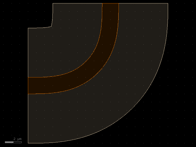
@gf.cell
def tline_bend_circular(
    radius: float = 10,
    angle: float = 90,
    signal_cross_section: CrossSectionSpec = "topmetal2_routing",
    ground_cross_section: CrossSectionSpec = "topmetal1_routing",
    width: float | None = None,
    Z0: float | None = None,
) -> gf.Component:
    """Returns a circular bend coplanar transmission line.

    Creates a signal bend and a wider ground bend aligned around it.

    Args:
        radius: Bend radius (um).
        angle: Bend angle (degrees).
        signal_cross_section: Cross-section for the signal line.
        ground_cross_section: Cross-section for the ground line.
        width: Line width (µm). Mutually exclusive with Z0.
        Z0: Target characteristic impedance (ohms). Mutually exclusive with width.
    """

    width, Z0 = _resolve_tline_width_and_Z0(
        width=width,
        Z0=Z0,
        signal_cross_section=signal_cross_section,
        ground_cross_section=ground_cross_section,
    )

    c = gf.Component()

    if angle == 90 or angle == 180:
        signal = c.add_ref(
            gf.c.bend_circular(
                radius=radius,
                angle=angle,
                cross_section=signal_cross_section,
                width=width,
                allow_min_radius_violation=True,
            )
        )
        c.add_ports(signal.ports)
        c.add_ref(
            gf.c.bend_circular(
                radius=radius,
                angle=angle,
                cross_section=ground_cross_section,
                width=7 * width,
                allow_min_radius_violation=True,
            )
        )
    else:
        signal = c.add_ref_off_grid(
            gf.c.bend_circular_all_angle(
                radius=radius,
                angle=angle,
                cross_section=signal_cross_section,
                width=width,
                allow_min_radius_violation=True,
            )
        )
        c.add_ports(signal.ports)
        c.add_ref_off_grid(
            gf.c.bend_circular_all_angle(
                radius=radius,
                angle=angle,
                cross_section=ground_cross_section,
                width=7 * width,
                allow_min_radius_violation=True,
            )
        )

    return c

tline_bend_circular

import warnings
warnings.filterwarnings("ignore", category=DeprecationWarning)

from ihp import PDK
from ihp import cells

PDK.activate()

c = cells.tline_bend_circular(radius=10, angle=90, signal_cross_section='topmetal2_routing', ground_cross_section='topmetal1_routing').copy()
c.draw_ports()
c.plot()

tline_bend_euler

Returns an euler bend coplanar transmission line.

Creates a signal bend and a wider ground bend aligned around it.

Parameters:

Name Type Description Default
radius float

Bend radius (um).

10
angle float

Bend angle (degrees).

90
signal_cross_section CrossSection | str | dict[str, Any] | Callable[..., CrossSection] | SymmetricalCrossSection | DCrossSection

Cross-section for the signal line.

'topmetal2_routing'
ground_cross_section CrossSection | str | dict[str, Any] | Callable[..., CrossSection] | SymmetricalCrossSection | DCrossSection

Cross-section for the ground line.

'topmetal1_routing'
width float | None

Line width (µm). Mutually exclusive with Z0.

None
Z0 float | None

Target characteristic impedance (ohms). Mutually exclusive with width.

None
Source code in ihp/cells/waveguides.py
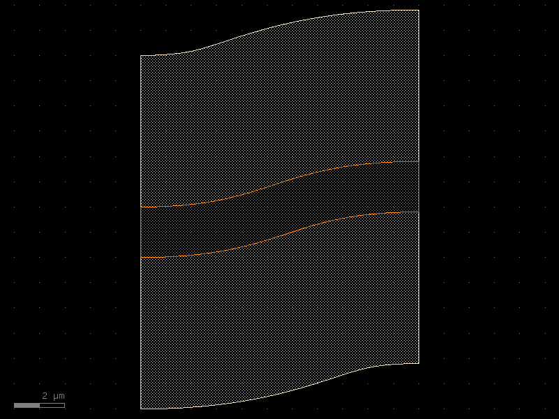
@gf.cell
def tline_bend_euler(
    radius: float = 10,
    angle: float = 90,
    signal_cross_section: CrossSectionSpec = "topmetal2_routing",
    ground_cross_section: CrossSectionSpec = "topmetal1_routing",
    width: float | None = None,
    Z0: float | None = None,
) -> gf.Component:
    """Returns an euler bend coplanar transmission line.

    Creates a signal bend and a wider ground bend aligned around it.

    Args:
        radius: Bend radius (um).
        angle: Bend angle (degrees).
        signal_cross_section: Cross-section for the signal line.
        ground_cross_section: Cross-section for the ground line.
        width: Line width (µm). Mutually exclusive with Z0.
        Z0: Target characteristic impedance (ohms). Mutually exclusive with width.
    """

    width, Z0 = _resolve_tline_width_and_Z0(
        width=width,
        Z0=Z0,
        signal_cross_section=signal_cross_section,
        ground_cross_section=ground_cross_section,
    )

    c = gf.Component()

    if angle == 90 or angle == 180:
        signal = c.add_ref(
            gf.c.bend_euler(
                radius=radius,
                angle=angle,
                cross_section=signal_cross_section,
                width=width,
                allow_min_radius_violation=True,
            )
        )
        c.add_ports(signal.ports)
        c.add_ref(
            gf.c.bend_euler(
                radius=radius,
                angle=angle,
                cross_section=ground_cross_section,
                width=7 * width,
                allow_min_radius_violation=True,
            )
        )
    else:
        signal = c.add_ref_off_grid(
            gf.c.bend_euler_all_angle(
                radius=radius,
                angle=angle,
                cross_section=signal_cross_section,
                width=width,
                allow_min_radius_violation=True,
            )
        )
        c.add_ports(signal.ports)
        c.add_ref_off_grid(
            gf.c.bend_euler_all_angle(
                radius=radius,
                angle=angle,
                cross_section=ground_cross_section,
                width=7 * width,
                allow_min_radius_violation=True,
            )
        )

    return c

tline_bend_euler

import warnings
warnings.filterwarnings("ignore", category=DeprecationWarning)

from ihp import PDK
from ihp import cells

PDK.activate()

c = cells.tline_bend_euler(radius=10, angle=90, signal_cross_section='topmetal2_routing', ground_cross_section='topmetal1_routing').copy()
c.draw_ports()
c.plot()

tline_bend_s

Returns an S bend coplanar transmission line.

Creates a signal bend and a wider ground bend aligned around it.

Parameters:

Name Type Description Default
size tuple[float, float]

in x and y direction.

(11, 1.8)
signal_cross_section CrossSection | str | dict[str, Any] | Callable[..., CrossSection] | SymmetricalCrossSection | DCrossSection

Cross-section for the signal line.

'topmetal2_routing'
ground_cross_section CrossSection | str | dict[str, Any] | Callable[..., CrossSection] | SymmetricalCrossSection | DCrossSection

Cross-section for the ground line.

'topmetal1_routing'
width float | None

Line width (µm). Mutually exclusive with Z0.

None
Z0 float | None

Target characteristic impedance (ohms). Mutually exclusive with width.

None
Source code in ihp/cells/waveguides.py
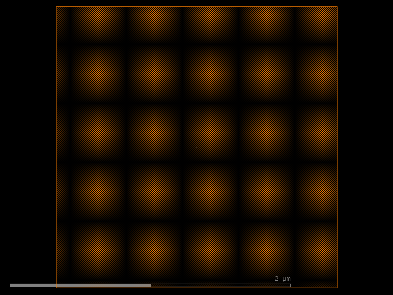
@gf.cell
def tline_bend_s(
    size: Size = (11, 1.8),
    signal_cross_section: CrossSectionSpec = "topmetal2_routing",
    ground_cross_section: CrossSectionSpec = "topmetal1_routing",
    width: float | None = None,
    Z0: float | None = None,
) -> gf.Component:
    """Returns an S bend coplanar transmission line.

    Creates a signal bend and a wider ground bend aligned around it.

    Args:
        size: in x and y direction.
        signal_cross_section: Cross-section for the signal line.
        ground_cross_section: Cross-section for the ground line.
        width: Line width (µm). Mutually exclusive with Z0.
        Z0: Target characteristic impedance (ohms). Mutually exclusive with width.
    """

    width, Z0 = _resolve_tline_width_and_Z0(
        width=width,
        Z0=Z0,
        signal_cross_section=signal_cross_section,
        ground_cross_section=ground_cross_section,
    )

    c = gf.Component()

    signal = c.add_ref(
        gf.c.bend_s(
            size=size,
            cross_section=signal_cross_section,
            width=width,
            allow_min_radius_violation=True,
        )
    )
    c.add_ports(signal.ports)
    c.add_ref(
        gf.c.bend_s(
            size=(size),
            cross_section=ground_cross_section,
            width=7 * width,
            allow_min_radius_violation=True,
        )
    )

    return c

tline_bend_s

import warnings
warnings.filterwarnings("ignore", category=DeprecationWarning)

from ihp import PDK
from ihp import cells

PDK.activate()

c = cells.tline_bend_s(size=(11, 1.8), signal_cross_section='topmetal2_routing', ground_cross_section='topmetal1_routing').copy()
c.draw_ports()
c.plot()

tline_corner

Return a right-angle corner transition for a transmission line.

Parameters:

Name Type Description Default
length float

Reserved parameter for API compatibility.

10
signal_cross_section CrossSection | str | dict[str, Any] | Callable[..., CrossSection] | SymmetricalCrossSection | DCrossSection

Cross-section for the signal line.

'topmetal2_routing'
ground_cross_section CrossSection | str | dict[str, Any] | Callable[..., CrossSection] | SymmetricalCrossSection | DCrossSection | list[CrossSection | str | dict[str, Any] | Callable[..., CrossSection] | SymmetricalCrossSection | DCrossSection]

Ground cross-section, or [lower, upper] for stripline.

'topmetal1_routing'
width float | None

Signal width in um. Mutually exclusive with Z0.

None
Z0 float | None

Target characteristic impedance in ohms. Mutually exclusive with width.

None

Returns:

Type Description
Component

A corner component with four electrical ports.

Source code in ihp/cells/waveguides.py
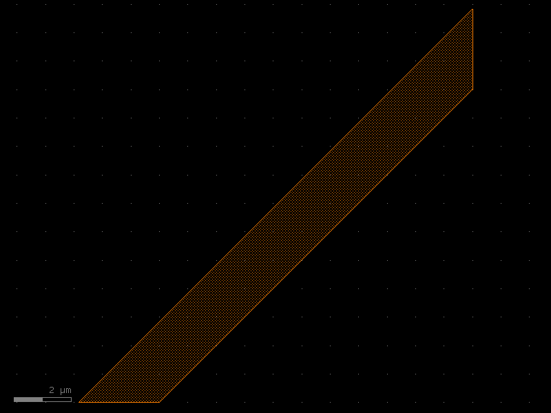
@gf.cell
def tline_corner(
    length: float = 10,
    signal_cross_section: CrossSectionSpec = "topmetal2_routing",
    ground_cross_section: CrossSectionSpec
    | list[CrossSectionSpec] = "topmetal1_routing",
    width: float | None = None,
    Z0: float | None = None,
) -> gf.Component:
    """Return a right-angle corner transition for a transmission line.

    Args:
        length: Reserved parameter for API compatibility.
        signal_cross_section: Cross-section for the signal line.
        ground_cross_section: Ground cross-section, or ``[lower, upper]``
            for stripline.
        width: Signal width in um. Mutually exclusive with ``Z0``.
        Z0: Target characteristic impedance in ohms. Mutually exclusive
            with ``width``.

    Returns:
        A corner component with four electrical ports.
    """
    width, Z0 = _resolve_tline_width_and_Z0(
        width=width,
        Z0=Z0,
        signal_cross_section=signal_cross_section,
        ground_cross_section=ground_cross_section,
    )

    c = gf.Component()
    # signal
    c.add_polygon(
        points=[(0, 0), (0, width), (width, width), (width, 0)],
        layer=gf.get_cross_section(signal_cross_section).layer,
    )

    extension = 3  # extension over signal plate
    if isinstance(ground_cross_section, list):
        # ground planes for stripline
        for gc in ground_cross_section:
            c.add_polygon(
                points=[
                    (0 - extension * width, -extension * width),
                    (0 - extension * width, width + extension * width),
                    (width + extension * width, width + extension * width),
                    (width + extension * width, 0 - extension * width),
                ],
                layer=gf.get_cross_section(gc).layer,
            )
    else:
        # ground plate
        c.add_polygon(
            points=[
                (0 - extension * width, -extension * width),
                (0 - extension * width, width + extension * width),
                (width + extension * width, width + extension * width),
                (width + extension * width, 0 - extension * width),
            ],
            layer=gf.get_cross_section(ground_cross_section).layer,
        )

    c.add_port(
        name="e1",
        center=(0, width / 2),
        width=width,
        orientation=180,
        port_type="electrical",
        layer=gf.get_cross_section(signal_cross_section).layer,
    )
    c.add_port(
        name="e2",
        center=(width / 2, width),
        width=width,
        orientation=90,
        port_type="electrical",
        layer=gf.get_cross_section(signal_cross_section).layer,
    )
    c.add_port(
        name="e3",
        center=(width, width / 2),
        width=width,
        orientation=0,
        port_type="electrical",
        layer=gf.get_cross_section(signal_cross_section).layer,
    )
    c.add_port(
        name="e4",
        center=(width / 2, 0),
        width=width,
        orientation=270,
        port_type="electrical",
        layer=gf.get_cross_section(signal_cross_section).layer,
    )
    return c

tline_corner

import warnings
warnings.filterwarnings("ignore", category=DeprecationWarning)

from ihp import PDK
from ihp import cells

PDK.activate()

c = cells.tline_corner(length=10, signal_cross_section='topmetal2_routing', ground_cross_section='topmetal1_routing').copy()
c.draw_ports()
c.plot()

via_array

Create an array of vias.

Parameters:

Name Type Description Default
via_type str

Type of via (Via1, Via2, Via3, Via4, TopVia1, TopVia2).

'Via1'
columns int

Number of via columns.

2
rows int

Number of via rows.

2
via_size float | None

Via size in micrometers (uses default if None).

None
via_spacing float | None

Via spacing in micrometers (uses default if None).

None
via_enclosure float | None

Metal enclosure in micrometers (uses default if None).

None
layer_via1 tuple[int, int] | str | int | LayerEnum

Via1 layer.

'Via1drawing'
layer_via2 tuple[int, int] | str | int | LayerEnum

Via2 layer.

'Via2drawing'
layer_via3 tuple[int, int] | str | int | LayerEnum

Via3 layer.

'Via3drawing'
layer_via4 tuple[int, int] | str | int | LayerEnum

Via4 layer.

'Via4drawing'
layer_topvia1 tuple[int, int] | str | int | LayerEnum

TopVia1 layer.

'TopVia1drawing'
layer_topvia2 tuple[int, int] | str | int | LayerEnum

TopVia2 layer.

'TopVia2drawing'

Returns:

Type Description
Component

Component with via array.

Source code in ihp/cells/via_stacks.py
@gf.cell(tags=["IHP", "via", "array"])
def via_array(
    via_type: str = "Via1",
    columns: int = 2,
    rows: int = 2,
    via_size: float | None = None,
    via_spacing: float | None = None,
    via_enclosure: float | None = None,
    layer_cont: LayerSpec = "Contdrawing",
    layer_via1: LayerSpec = "Via1drawing",
    layer_via2: LayerSpec = "Via2drawing",
    layer_via3: LayerSpec = "Via3drawing",
    layer_via4: LayerSpec = "Via4drawing",
    layer_vmim: LayerSpec = "Vmimdrawing",
    layer_topvia1: LayerSpec = "TopVia1drawing",
    layer_topvia2: LayerSpec = "TopVia2drawing",
) -> Component:
    """Create an array of vias.

    Args:
        via_type: Type of via (Via1, Via2, Via3, Via4, TopVia1, TopVia2).
        columns: Number of via columns.
        rows: Number of via rows.
        via_size: Via size in micrometers (uses default if None).
        via_spacing: Via spacing in micrometers (uses default if None).
        via_enclosure: Metal enclosure in micrometers (uses default if None).
        layer_via1: Via1 layer.
        layer_via2: Via2 layer.
        layer_via3: Via3 layer.
        layer_via4: Via4 layer.
        layer_topvia1: TopVia1 layer.
        layer_topvia2: TopVia2 layer.

    Returns:
        Component with via array.
    """
    c = Component()

    # Map via type to layer parameter
    via_layer_map = {
        "Cont": layer_cont,
        "Via1": layer_via1,
        "Via2": layer_via2,
        "Via3": layer_via3,
        "Via4": layer_via4,
        "Vmim": layer_vmim,
        "TopVia1": layer_topvia1,
        "TopVia2": layer_topvia2,
    }

    # Get via parameters
    if via_type not in via_layer_map:
        raise ValueError(f"Unknown via type: {via_type}")

    via_layer = via_layer_map[via_type]
    rules = VIA_RULES[via_type]

    # Use provided values or defaults
    size = via_size if via_size is not None else rules["size"]
    spacing = via_spacing if via_spacing is not None else rules["spacing"]
    enclosure = via_enclosure if via_enclosure is not None else rules["enclosure"]

    # Create via array
    for col in range(columns):
        for row in range(rows):
            x = col * spacing
            y = row * spacing

            via = gf.components.rectangle(
                size=(size, size),
                layer=via_layer,
            )
            via_ref = c.add_ref(via)
            via_ref.move((x, y))

    # Calculate total dimensions
    array_width = size if columns == 1 else (columns - 1) * spacing + size
    array_height = size if rows == 1 else (rows - 1) * spacing + size

    # Add metadata
    c.info["via_type"] = via_type
    c.info["columns"] = columns
    c.info["rows"] = rows
    c.info["array_width"] = array_width
    c.info["array_height"] = array_height
    c.info["enclosure_width"] = array_width + 2 * enclosure
    c.info["enclosure_height"] = array_height + 2 * enclosure

    return c

via_array

import warnings
warnings.filterwarnings("ignore", category=DeprecationWarning)

from ihp import PDK
from ihp import cells

PDK.activate()

c = cells.via_array(via_type='Via1', columns=2, rows=2, layer_cont='Contdrawing', layer_via1='Via1drawing', layer_via2='Via2drawing', layer_via3='Via3drawing', layer_via4='Via4drawing', layer_vmim='Vmimdrawing', layer_topvia1='TopVia1drawing', layer_topvia2='TopVia2drawing').copy()
c.draw_ports()
c.plot()

via_stack

Create a via stack connecting multiple metal layers.

bottom_layer can be Activ, GatPoly, or any metal (Metal1-TopMetal2). Activ and GatPoly connect to Metal1 through Cont; they are independent paths and must not appear together in the same stack.

Parameters:

Name Type Description Default
bottom_layer str

Bottom layer name (Activ, GatPoly, or Metal1-TopMetal2).

'Metal1'
top_layer str

Top metal layer name (Metal1-TopMetal2).

'Metal2'
size tuple[float, float]

Size of the metal stack (width, height) in micrometers.

(10.0, 10.0)
vn_columns int

Number of columns for normal vias (Cont, Via1-Via4).

2
vn_rows int

Number of rows for normal vias.

2
vt1_columns int

Number of columns for TopVia1.

1
vt1_rows int

Number of rows for TopVia1.

1
vt2_columns int

Number of columns for TopVia2.

1
vt2_rows int

Number of rows for TopVia2.

1

Returns:

Type Description
Component

Component with via stack.

Source code in ihp/cells/via_stacks.py
@gf.cell(tags=["IHP", "via", "stack"])
def via_stack(
    bottom_layer: str = "Metal1",
    top_layer: str = "Metal2",
    size: tuple[float, float] = (10.0, 10.0),
    vn_columns: int = 2,
    vn_rows: int = 2,
    vt1_columns: int = 1,
    vt1_rows: int = 1,
    vt2_columns: int = 1,
    vt2_rows: int = 1,
    layer_activ: LayerSpec = "Activdrawing",
    layer_gatpoly: LayerSpec = "GatPolydrawing",
    layer_metal1: LayerSpec = "Metal1drawing",
    layer_metal2: LayerSpec = "Metal2drawing",
    layer_metal3: LayerSpec = "Metal3drawing",
    layer_metal4: LayerSpec = "Metal4drawing",
    layer_metal5: LayerSpec = "Metal5drawing",
    layer_topmetal1: LayerSpec = "TopMetal1drawing",
    layer_topmetal2: LayerSpec = "TopMetal2drawing",
    layer_activ_pin: LayerSpec = "Activpin",
    layer_gatpoly_pin: LayerSpec = "GatPolypin",
    layer_metal1_pin: LayerSpec = "Metal1pin",
    layer_metal2_pin: LayerSpec = "Metal2pin",
    layer_metal3_pin: LayerSpec = "Metal3pin",
    layer_metal4_pin: LayerSpec = "Metal4pin",
    layer_metal5_pin: LayerSpec = "Metal5pin",
    layer_topmetal1_pin: LayerSpec = "TopMetal1pin",
    layer_topmetal2_pin: LayerSpec = "TopMetal2pin",
    layer_cont: LayerSpec = "Contdrawing",
    layer_via1: LayerSpec = "Via1drawing",
    layer_via2: LayerSpec = "Via2drawing",
    layer_via3: LayerSpec = "Via3drawing",
    layer_via4: LayerSpec = "Via4drawing",
    layer_topvia1: LayerSpec = "TopVia1drawing",
    layer_topvia2: LayerSpec = "TopVia2drawing",
) -> Component:
    """Create a via stack connecting multiple metal layers.

    bottom_layer can be Activ, GatPoly, or any metal (Metal1-TopMetal2).
    Activ and GatPoly connect to Metal1 through Cont; they are independent
    paths and must not appear together in the same stack.

    Args:
        bottom_layer: Bottom layer name (Activ, GatPoly, or Metal1-TopMetal2).
        top_layer: Top metal layer name (Metal1-TopMetal2).
        size: Size of the metal stack (width, height) in micrometers.
        vn_columns: Number of columns for normal vias (Cont, Via1-Via4).
        vn_rows: Number of rows for normal vias.
        vt1_columns: Number of columns for TopVia1.
        vt1_rows: Number of rows for TopVia1.
        vt2_columns: Number of columns for TopVia2.
        vt2_rows: Number of rows for TopVia2.

    Returns:
        Component with via stack.
    """
    c = Component()

    # BEOL metal stack (Metal1 and above)
    _beol_order = [
        "Metal1",
        "Metal2",
        "Metal3",
        "Metal4",
        "Metal5",
        "TopMetal1",
        "TopMetal2",
    ]

    # Sub-Metal1 layers that connect to Metal1 via Cont
    _sub_metal1 = {"Activ", "GatPoly"}

    # Map layer names to layer parameters
    layer_map = {
        "Activ": layer_activ,
        "GatPoly": layer_gatpoly,
        "Metal1": layer_metal1,
        "Metal2": layer_metal2,
        "Metal3": layer_metal3,
        "Metal4": layer_metal4,
        "Metal5": layer_metal5,
        "TopMetal1": layer_topmetal1,
        "TopMetal2": layer_topmetal2,
    }

    pin_layer_map = {
        "Activ": layer_activ_pin,
        "GatPoly": layer_gatpoly_pin,
        "Metal1": layer_metal1_pin,
        "Metal2": layer_metal2_pin,
        "Metal3": layer_metal3_pin,
        "Metal4": layer_metal4_pin,
        "Metal5": layer_metal5_pin,
        "TopMetal1": layer_topmetal1_pin,
        "TopMetal2": layer_topmetal2_pin,
    }

    # Normalize layer names (case-insensitive match against known names)
    _all_names = {n.lower(): n for n in _beol_order + list(_sub_metal1)}
    bottom_port_label = bottom_layer
    top_port_label = top_layer
    bottom_layer = _all_names.get(bottom_layer.lower(), bottom_layer)
    top_layer = _all_names.get(top_layer.lower(), top_layer)

    # Build effective layer order based on bottom_layer
    if bottom_layer in _sub_metal1:
        # Activ or GatPoly -> Cont -> Metal1 -> ... -> top_layer
        if top_layer in _sub_metal1:
            raise ValueError(
                f"Cannot stack between two sub-Metal1 layers: "
                f"{bottom_layer} -> {top_layer}"
            )
        if top_layer not in _beol_order:
            raise ValueError(f"Invalid top layer: {top_layer}")
        top_idx = _beol_order.index(top_layer)
        layer_order = [bottom_layer] + _beol_order[: top_idx + 1]
    else:
        if bottom_layer not in _beol_order:
            raise ValueError(f"Invalid bottom layer: {bottom_layer}")
        if top_layer not in _beol_order:
            raise ValueError(f"Invalid top layer: {top_layer}")
        bottom_idx = _beol_order.index(bottom_layer)
        top_idx = _beol_order.index(top_layer)
        if bottom_idx > top_idx:
            raise ValueError(
                f"Bottom layer must be below top layer: {bottom_layer} -> {top_layer}"
            )
        layer_order = _beol_order[bottom_idx : top_idx + 1]

    width, height = size

    # Add conductor layers
    for name in layer_order:
        metal = gf.components.rectangle(
            size=(width, height),
            layer=layer_map[name],
            centered=True,
        )
        c.add_ref(metal)

    # Add vias between adjacent layers
    for i in range(len(layer_order) - 1):
        bot = layer_order[i]
        top = layer_order[i + 1]
        via_name = get_via_name(bot, top)

        if via_name is None:
            continue

        rules = VIA_RULES[via_name]
        via_size = rules["size"]
        via_spacing = rules["spacing"]
        via_enclosure = rules["enclosure"]

        # Determine number of vias based on type
        if via_name == "TopVia1":
            columns = vt1_columns
            rows = vt1_rows
        elif via_name == "TopVia2":
            columns = vt2_columns
            rows = vt2_rows
        else:
            columns = vn_columns
            rows = vn_rows

        # Calculate maximum number of vias that fit
        max_columns = int((width - 2 * via_enclosure - via_size) / via_spacing) + 1
        max_rows = int((height - 2 * via_enclosure - via_size) / via_spacing) + 1

        # Use minimum of requested and maximum
        actual_columns = min(columns, max_columns)
        actual_rows = min(rows, max_rows)

        if actual_columns > 0 and actual_rows > 0:
            via_array_comp = via_array(
                via_type=via_name,
                columns=actual_columns,
                rows=actual_rows,
                via_size=via_size,
                via_spacing=via_spacing,
                via_enclosure=via_enclosure,
                layer_cont=layer_cont,
                layer_via1=layer_via1,
                layer_via2=layer_via2,
                layer_via3=layer_via3,
                layer_via4=layer_via4,
                layer_topvia1=layer_topvia1,
                layer_topvia2=layer_topvia2,
            )

            # Center the via array
            array_width = via_array_comp.info["array_width"]
            array_height = via_array_comp.info["array_height"]

            via_ref = c.add_ref(via_array_comp)
            via_ref.move((-array_width / 2, -array_height / 2))

    # Add directional ports per layer (N/S/E/W at bbox edges)
    hx = width / 2
    hy = height / 2
    _port_specs = {
        "N": ((0, hy), 90, width),
        "S": ((0, -hy), 270, width),
        "E": ((hx, 0), 0, height),
        "W": ((-hx, 0), 180, height),
    }
    _port_layers = [(bottom_layer, bottom_port_label)]
    if top_layer != bottom_layer or top_port_label != bottom_port_label:
        _port_layers.append((top_layer, top_port_label))
    for layer_name, port_label in _port_layers:
        pin_layer = pin_layer_map[layer_name]
        for direction, (center, orientation, port_width) in _port_specs.items():
            c.add_port(
                name=f"{port_label}_{direction}",
                center=center,
                width=port_width,
                orientation=orientation,
                layer=pin_layer,
                port_type="electrical",
            )

    # Add metadata
    c.info["bottom_layer"] = bottom_layer
    c.info["top_layer"] = top_layer
    c.info["width"] = width
    c.info["height"] = height
    c.info["n_layers"] = len(layer_order)

    return c

via_stack

import warnings
warnings.filterwarnings("ignore", category=DeprecationWarning)

from ihp import PDK
from ihp import cells

PDK.activate()

c = cells.via_stack(bottom_layer='Metal1', top_layer='Metal2', size=(10.0, 10.0), vn_columns=2, vn_rows=2, vt1_columns=1, vt1_rows=1, vt2_columns=1, vt2_rows=1, layer_activ='Activdrawing', layer_gatpoly='GatPolydrawing', layer_metal1='Metal1drawing', layer_metal2='Metal2drawing', layer_metal3='Metal3drawing', layer_metal4='Metal4drawing', layer_metal5='Metal5drawing', layer_topmetal1='TopMetal1drawing', layer_topmetal2='TopMetal2drawing', layer_activ_pin='Activpin', layer_gatpoly_pin='GatPolypin', layer_metal1_pin='Metal1pin', layer_metal2_pin='Metal2pin', layer_metal3_pin='Metal3pin', layer_metal4_pin='Metal4pin', layer_metal5_pin='Metal5pin', layer_topmetal1_pin='TopMetal1pin', layer_topmetal2_pin='TopMetal2pin', layer_cont='Contdrawing', layer_via1='Via1drawing', layer_via2='Via2drawing', layer_via3='Via3drawing', layer_via4='Via4drawing', layer_topvia1='TopVia1drawing', layer_topvia2='TopVia2drawing').copy()
c.draw_ports()
c.plot()

via_stack_with_pads

Create a via stack with test pads.

Parameters:

Name Type Description Default
bottom_layer str

Bottom layer name (Activ, GatPoly, or Metal1-TopMetal2).

'Metal1'
top_layer str

Top metal layer name (Metal1-TopMetal2).

'TopMetal2'
size tuple[float, float]

Size of the via stack (width, height) in micrometers.

(10.0, 10.0)
pad_size tuple[float, float]

Size of the test pads (width, height) in micrometers.

(20.0, 20.0)
pad_spacing float

Spacing between pads in micrometers.

50.0

Returns:

Type Description
Component

Component with via stack and test pads.

Source code in ihp/cells/via_stacks.py
@gf.cell(tags=["IHP", "via", "stack"])
def via_stack_with_pads(
    bottom_layer: str = "Metal1",
    top_layer: str = "TopMetal2",
    size: tuple[float, float] = (10.0, 10.0),
    pad_size: tuple[float, float] = (20.0, 20.0),
    pad_spacing: float = 50.0,
    layer_activ: LayerSpec = "Activdrawing",
    layer_gatpoly: LayerSpec = "GatPolydrawing",
    layer_metal1: LayerSpec = "Metal1drawing",
    layer_metal2: LayerSpec = "Metal2drawing",
    layer_metal3: LayerSpec = "Metal3drawing",
    layer_metal4: LayerSpec = "Metal4drawing",
    layer_metal5: LayerSpec = "Metal5drawing",
    layer_topmetal1: LayerSpec = "TopMetal1drawing",
    layer_topmetal2: LayerSpec = "TopMetal2drawing",
    layer_activ_pin: LayerSpec = "Activpin",
    layer_gatpoly_pin: LayerSpec = "GatPolypin",
    layer_metal1_pin: LayerSpec = "Metal1pin",
    layer_metal2_pin: LayerSpec = "Metal2pin",
    layer_metal3_pin: LayerSpec = "Metal3pin",
    layer_metal4_pin: LayerSpec = "Metal4pin",
    layer_metal5_pin: LayerSpec = "Metal5pin",
    layer_topmetal1_pin: LayerSpec = "TopMetal1pin",
    layer_topmetal2_pin: LayerSpec = "TopMetal2pin",
    layer_cont: LayerSpec = "Contdrawing",
    layer_via1: LayerSpec = "Via1drawing",
    layer_via2: LayerSpec = "Via2drawing",
    layer_via3: LayerSpec = "Via3drawing",
    layer_via4: LayerSpec = "Via4drawing",
    layer_topvia1: LayerSpec = "TopVia1drawing",
    layer_topvia2: LayerSpec = "TopVia2drawing",
) -> Component:
    """Create a via stack with test pads.

    Args:
        bottom_layer: Bottom layer name (Activ, GatPoly, or Metal1-TopMetal2).
        top_layer: Top metal layer name (Metal1-TopMetal2).
        size: Size of the via stack (width, height) in micrometers.
        pad_size: Size of the test pads (width, height) in micrometers.
        pad_spacing: Spacing between pads in micrometers.

    Returns:
        Component with via stack and test pads.
    """
    c = Component()

    # Map layer names to layer parameters
    layer_map = {
        "Activ": layer_activ,
        "GatPoly": layer_gatpoly,
        "Metal1": layer_metal1,
        "Metal2": layer_metal2,
        "Metal3": layer_metal3,
        "Metal4": layer_metal4,
        "Metal5": layer_metal5,
        "TopMetal1": layer_topmetal1,
        "TopMetal2": layer_topmetal2,
    }

    pin_layer_map = {
        "Activ": layer_activ_pin,
        "GatPoly": layer_gatpoly_pin,
        "Metal1": layer_metal1_pin,
        "Metal2": layer_metal2_pin,
        "Metal3": layer_metal3_pin,
        "Metal4": layer_metal4_pin,
        "Metal5": layer_metal5_pin,
        "TopMetal1": layer_topmetal1_pin,
        "TopMetal2": layer_topmetal2_pin,
    }

    # Create via stack
    stack = via_stack(
        bottom_layer=bottom_layer,
        top_layer=top_layer,
        size=size,
        layer_activ=layer_activ,
        layer_gatpoly=layer_gatpoly,
        layer_metal1=layer_metal1,
        layer_metal2=layer_metal2,
        layer_metal3=layer_metal3,
        layer_metal4=layer_metal4,
        layer_metal5=layer_metal5,
        layer_topmetal1=layer_topmetal1,
        layer_topmetal2=layer_topmetal2,
        layer_activ_pin=layer_activ_pin,
        layer_gatpoly_pin=layer_gatpoly_pin,
        layer_metal1_pin=layer_metal1_pin,
        layer_metal2_pin=layer_metal2_pin,
        layer_metal3_pin=layer_metal3_pin,
        layer_metal4_pin=layer_metal4_pin,
        layer_metal5_pin=layer_metal5_pin,
        layer_topmetal1_pin=layer_topmetal1_pin,
        layer_topmetal2_pin=layer_topmetal2_pin,
        layer_cont=layer_cont,
        layer_via1=layer_via1,
        layer_via2=layer_via2,
        layer_via3=layer_via3,
        layer_via4=layer_via4,
        layer_topvia1=layer_topvia1,
        layer_topvia2=layer_topvia2,
    )
    c.add_ref(stack)

    # Add bottom pad
    bottom_pad = gf.components.rectangle(
        size=pad_size,
        layer=layer_map[bottom_layer],
        centered=True,
    )
    bottom_pad_ref = c.add_ref(bottom_pad)
    bottom_pad_ref.movex(-pad_spacing / 2)

    # Add top pad
    top_pad = gf.components.rectangle(
        size=pad_size,
        layer=layer_map[top_layer],
        centered=True,
    )
    top_pad_ref = c.add_ref(top_pad)
    top_pad_ref.movex(pad_spacing / 2)

    # Connect pads to stack
    bottom_trace = gf.components.rectangle(
        size=(pad_spacing / 2 - size[0] / 2, 2.0),
        layer=layer_map[bottom_layer],
    )
    bottom_trace_ref = c.add_ref(bottom_trace)
    bottom_trace_ref.move((-pad_spacing / 2, -1.0))

    top_trace = gf.components.rectangle(
        size=(pad_spacing / 2 - size[0] / 2, 2.0),
        layer=layer_map[top_layer],
    )
    top_trace_ref = c.add_ref(top_trace)
    top_trace_ref.move((size[0] / 2, -1.0))

    # Add ports
    c.add_port(
        name="pad1",
        center=(-pad_spacing / 2, 0),
        width=pad_size[1],
        orientation=180,
        layer=pin_layer_map[bottom_layer],
        port_type="electrical",
    )

    c.add_port(
        name="pad2",
        center=(pad_spacing / 2, 0),
        width=pad_size[1],
        orientation=0,
        layer=pin_layer_map[top_layer],
        port_type="electrical",
    )

    return c

via_stack_with_pads

import warnings
warnings.filterwarnings("ignore", category=DeprecationWarning)

from ihp import PDK
from ihp import cells

PDK.activate()

c = cells.via_stack_with_pads(bottom_layer='Metal1', top_layer='TopMetal2', size=(10.0, 10.0), pad_size=(20.0, 20.0), pad_spacing=50.0, layer_activ='Activdrawing', layer_gatpoly='GatPolydrawing', layer_metal1='Metal1drawing', layer_metal2='Metal2drawing', layer_metal3='Metal3drawing', layer_metal4='Metal4drawing', layer_metal5='Metal5drawing', layer_topmetal1='TopMetal1drawing', layer_topmetal2='TopMetal2drawing', layer_activ_pin='Activpin', layer_gatpoly_pin='GatPolypin', layer_metal1_pin='Metal1pin', layer_metal2_pin='Metal2pin', layer_metal3_pin='Metal3pin', layer_metal4_pin='Metal4pin', layer_metal5_pin='Metal5pin', layer_topmetal1_pin='TopMetal1pin', layer_topmetal2_pin='TopMetal2pin', layer_cont='Contdrawing', layer_via1='Via1drawing', layer_via2='Via2drawing', layer_via3='Via3drawing', layer_via4='Via4drawing', layer_topvia1='TopVia1drawing', layer_topvia2='TopVia2drawing').copy()
c.draw_ports()
c.plot()

wilkinson_power_divider

Return a Wilkinson power divider coplanar transmission line.

Constructs a two-way Wilkinson divider from quarter-wave transformer branches (impedance \(Z_0 / sqrt{2}\)) arranged in a loop. The quarter-wave length is derived from frequency and the effective dielectric constant of the selected cross-section stack.

Parameters:

Name Type Description Default
connection_length float

Length of the input/output feed lines (um).

50
frequency float

Operating frequency (Hz).

30000000000.0
Z0 float

Target characteristic impedance of the input/output ports (ohms).

50
signal_cross_section CrossSection | str | dict[str, Any] | Callable[..., CrossSection] | SymmetricalCrossSection | DCrossSection

Cross-section for the signal line.

'topmetal2_routing'
ground_cross_section CrossSection | str | dict[str, Any] | Callable[..., CrossSection] | SymmetricalCrossSection | DCrossSection | list[CrossSection | str | dict[str, Any] | Callable[..., CrossSection] | SymmetricalCrossSection | DCrossSection]

Cross-section for the ground line. Accepts a single spec for microstrip or a two-element list [lower, upper] for stripline.

'topmetal1_routing'
shape str

Shape of the Wilkinson divider. Can be either "C" or "U". In a "C" shape, the quarter-wave branches are connected in a loop, while in a "U" shape, the branches are not braught together again

'C'

Returns: A Component containing the Wilkinson power divider with ports e1 (input), e2 and e3 (outputs).

Source code in ihp/cells/rf_devices.py
236
237
238
239
240
241
242
243
244
245
246
247
248
249
250
251
252
253
254
255
256
257
258
259
260
261
262
263
264
265
266
267
268
269
270
271
272
273
274
275
276
277
278
279
280
281
282
283
284
285
286
287
288
289
290
291
292
293
294
295
296
297
298
299
300
301
302
303
304
305
306
307
308
309
310
311
312
313
314
315
316
317
318
319
320
321
322
323
324
325
326
327
328
329
330
331
332
333
334
335
336
337
338
339
340
341
342
343
344
345
346
347
348
349
350
351
352
353
354
355
356
357
358
359
360
361
362
363
364
365
366
367
368
369
370
371
372
373
374
375
376
377
378
379
380
381
382
383
384
385
386
387
388
389
390
391
392
393
394
395
396
397
398
399
400
401
402
403
404
405
406
407
408
409
410
411
412
413
414
415
416
417
418
419
420
421
422
423
424
425
426
427
428
429
430
431
432
433
434
435
436
437
438
439
440
441
442
443
444
445
446
447
448
449
450
451
452
453
454
455
456
457
458
459
460
461
462
463
464
465
466
467
468
469
470
471
472
473
474
475
476
477
478
479
480
481
482
483
484
485
486
487
488
489
490
491
492
493
494
495
496
497
498
499
500
501
502
503
504
505
506
507
508
509
510
511
512
513
514
515
516
517
518
519
520
521
522
523
524
525
526
527
528
529
530
531
532
533
534
535
536
537
538
539
540
541
542
543
544
545
546
547
548
549
550
551
552
553
554
555
556
557
558
559
560
561
562
563
564
565
566
567
568
569
570
571
572
573
574
575
576
577
578
579
580
581
582
583
584
585
586
587
588
589
590
591
592
593
594
595
596
597
598
599
600
601
602
603
604
605
606
607
608
609
610
611
612
613
614
615
616
617
618
619
620
621
622
623
624
625
626
627
628
629
630
631
632
633
634
635
@gf.cell
def wilkinson_power_divider(
    connection_length: float = 50,
    frequency: float = 30e9,
    Z0: float = 50,
    signal_cross_section: CrossSectionSpec = "topmetal2_routing",
    ground_cross_section: CrossSectionSpec
    | list[CrossSectionSpec] = "topmetal1_routing",
    shape: str = "C",
    e_r: float = 4.1,
) -> gf.Component:
    """Return a Wilkinson power divider coplanar transmission line.

    Constructs a two-way Wilkinson divider from quarter-wave transformer
    branches (impedance $Z_0 / sqrt{2}$) arranged in a loop.  The
    quarter-wave length is derived from *frequency* and the effective
    dielectric constant of the selected cross-section stack.

    Args:
        connection_length: Length of the input/output feed lines (um).
        frequency: Operating frequency (Hz).
        Z0: Target characteristic impedance of the input/output ports
            (ohms).
        signal_cross_section: Cross-section for the signal line.
        ground_cross_section: Cross-section for the ground line.
            Accepts a single spec for microstrip or a two-element list
            ``[lower, upper]`` for stripline.
        shape: Shape of the Wilkinson divider. Can be either "C" or "U". In a "C" shape, the quarter-wave branches are connected in a loop, while in a "U" shape, the branches are not braught together again
    Returns:
        A Component containing the Wilkinson power divider with ports
        ``e1`` (input), ``e2`` and ``e3`` (outputs).
    """

    c = gf.Component()

    # calculate the needed widths
    width_Z0 = _calculate_width_from_Z0(
        Z0=Z0,
        ground_cross_section=ground_cross_section,
        signal_cross_section=signal_cross_section,
        e_r=e_r,
    )
    width_Z0_sqrt2 = _calculate_width_from_Z0(
        Z0=Z0 * sqrt(2),
        ground_cross_section=ground_cross_section,
        signal_cross_section=signal_cross_section,
        e_r=e_r,
    )

    # create and connect the input line
    connection_in = c.add_ref(
        tline(
            length=connection_length,
            signal_cross_section=signal_cross_section,
            ground_cross_section=ground_cross_section,
            width=width_Z0,
        )
    )

    # calculate the quarter wave length for the given frequency and cross-section
    e_eff = _calculate_effective_dielectric_constant(
        signal_cross_section=signal_cross_section,
        ground_cross_section=ground_cross_section,
        e_r=e_r,
    )
    wave_length = (
        3e8 / frequency * 1e6 / sqrt(e_eff)
    )  # in um, assuming effective index of 3.5
    quater_wave_length = wave_length / 4
    quater_wave_length = quater_wave_length - quater_wave_length % (
        tech.nm
    )  # truncate to 5 nm

    # for future use
    width_R = 100
    length_R = _estimate_rppd_length(resistance_ohm=2 * Z0, width_um=width_R)

    # create and connect the corner piece for the connection line
    connection_corner = gf.Component()

    connection_corner.add_polygon(
        points=[(0, 0), (0, width_Z0), (width_Z0_sqrt2, width_Z0), (width_Z0_sqrt2, 0)],
        layer=gf.get_cross_section(signal_cross_section).layer,
    )
    connection_corner.add_port(
        name="e1",
        center=(0, width_Z0 / 2),
        width=width_Z0,
        orientation=180,
        port_type="electrical",
        layer=gf.get_cross_section(signal_cross_section).layer,
    )
    connection_corner.add_port(
        name="e2",
        center=(width_Z0_sqrt2 / 2, width_Z0),
        width=width_Z0_sqrt2,
        orientation=90,
        port_type="electrical",
        layer=gf.get_cross_section(signal_cross_section).layer,
    )
    connection_corner.add_port(
        name="e3",
        center=(width_Z0_sqrt2 / 2, 0),
        width=width_Z0_sqrt2,
        orientation=270,
        port_type="electrical",
        layer=gf.get_cross_section(signal_cross_section).layer,
    )

    connection_corner_ref = c.add_ref(connection_corner)

    connection_corner_ref.connect("e1", connection_in.ports["e2"])

    if shape == "C":
        # Calculate the circumference of the square
        circumference = quater_wave_length * 2 + length_R

        # create and connect upper branch line
        branch_left_up = c.add_ref(
            tline(
                length=circumference / 8 - width_Z0_sqrt2 - width_Z0 / 2,
                signal_cross_section=signal_cross_section,
                ground_cross_section=ground_cross_section,
                width=width_Z0_sqrt2,
            )
        )

        branch_left_up.connect("e1", connection_corner_ref.ports["e2"])

        corner_piece_upper_left = c.add_ref(
            tline_corner(
                signal_cross_section=signal_cross_section,
                ground_cross_section=ground_cross_section,
                Z0=Z0 * sqrt(2),
            )
        )
        corner_piece_upper_left.connect("e2", branch_left_up.ports["e2"])

        branch_left_down = c.add_ref(
            tline(
                length=circumference / 8 - width_Z0_sqrt2 - width_Z0 / 2,
                signal_cross_section=signal_cross_section,
                ground_cross_section=ground_cross_section,
                width=width_Z0_sqrt2,
            )
        )

        branch_left_down.connect("e1", connection_corner_ref.ports["e3"])

        corner_piece_lower_left = c.add_ref(
            tline_corner(
                signal_cross_section=signal_cross_section,
                ground_cross_section=ground_cross_section,
                Z0=Z0 * sqrt(2),
            )
        )
        corner_piece_lower_left.connect("e1", branch_left_down.ports["e2"])

        branch_top = c.add_ref(
            tline(
                length=circumference / 4 - width_Z0_sqrt2 * 2,
                signal_cross_section=signal_cross_section,
                ground_cross_section=ground_cross_section,
                width=width_Z0_sqrt2,
            )
        )

        branch_top.connect("e1", corner_piece_upper_left.ports["e1"])

        branch_bottom = c.add_ref(
            tline(
                length=circumference / 4 - width_Z0_sqrt2 * 2,
                signal_cross_section=signal_cross_section,
                ground_cross_section=ground_cross_section,
                width=width_Z0_sqrt2,
            )
        )

        branch_bottom.connect("e1", corner_piece_lower_left.ports["e2"])

        corner_piece_upper_right = c.add_ref(
            tline_corner(
                signal_cross_section=signal_cross_section,
                ground_cross_section=ground_cross_section,
                Z0=Z0 * sqrt(2),
            )
        )

        corner_piece_upper_right.connect("e2", branch_top.ports["e2"])

        branch_right_down = c.add_ref(
            tline(
                length=circumference / 8 - width_Z0_sqrt2 * 2 - length_R / 2,
                signal_cross_section=signal_cross_section,
                ground_cross_section=ground_cross_section,
                width=width_Z0_sqrt2,
            )
        )

        branch_right_down.connect("e1", corner_piece_upper_right.ports["e1"])

        corner_piece_lower_right = c.add_ref(
            tline_corner(
                signal_cross_section=signal_cross_section,
                ground_cross_section=ground_cross_section,
                Z0=Z0 * sqrt(2),
            )
        )
        corner_piece_lower_right.connect("e1", branch_bottom.ports["e2"])

        branch_right_up = c.add_ref(
            tline(
                length=circumference / 8 - width_Z0_sqrt2 * 2 - length_R / 2,
                signal_cross_section=signal_cross_section,
                ground_cross_section=ground_cross_section,
                width=width_Z0_sqrt2,
            )
        )

        branch_right_up.connect("e1", corner_piece_lower_right.ports["e2"])

        corner_output_p2 = c.add_ref(
            tline_corner(
                signal_cross_section=signal_cross_section,
                ground_cross_section=ground_cross_section,
                Z0=Z0 * sqrt(2),
            )
        )
        corner_output_p2.connect("e1", branch_right_down.ports["e2"])

        corner_output_p3 = c.add_ref(
            tline_corner(
                signal_cross_section=signal_cross_section,
                ground_cross_section=ground_cross_section,
                Z0=Z0 * sqrt(2),
            )
        )
        corner_output_p3.connect("e2", branch_right_up.ports["e2"])

        connection_out_p2 = c.add_ref(
            tline(
                length=connection_length,
                signal_cross_section=signal_cross_section,
                ground_cross_section=ground_cross_section,
                width=width_Z0,
            )
        )

        connection_out_p2.connect(
            "e1", corner_output_p2.ports["e2"], allow_width_mismatch=True
        )
        connection_out_p2.movey(width_Z0 / 2 - width_Z0_sqrt2 / 2)

        connection_out_p3 = c.add_ref(
            tline(
                length=connection_length,
                signal_cross_section=signal_cross_section,
                ground_cross_section=ground_cross_section,
                width=width_Z0,
            )
        )

        connection_out_p3.connect(
            "e1", corner_output_p3.ports["e1"], allow_width_mismatch=True
        )
        connection_out_p3.movey(-(width_Z0 / 2 - width_Z0_sqrt2 / 2))

        c.add_port(name="e1", port=connection_in.ports["e1"])
        c.add_port(name="e2", port=connection_out_p2.ports["e2"])
        c.add_port(name="e3", port=connection_out_p3.ports["e2"])

    elif shape == "U":
        # Calculate the circumference of the square
        circumference = quater_wave_length * 2

        # create and connect upper branch line
        branch_left_up = c.add_ref(
            tline(
                length=circumference / 6 - width_Z0_sqrt2 - width_Z0 / 2,
                signal_cross_section=signal_cross_section,
                ground_cross_section=ground_cross_section,
                width=width_Z0_sqrt2,
            )
        )

        branch_left_up.connect("e1", connection_corner_ref.ports["e2"])

        corner_piece_upper_left = c.add_ref(
            tline_corner(
                signal_cross_section=signal_cross_section,
                ground_cross_section=ground_cross_section,
                Z0=Z0 * sqrt(2),
            )
        )
        corner_piece_upper_left.connect("e2", branch_left_up.ports["e2"])

        branch_left_down = c.add_ref(
            tline(
                length=circumference / 6 - width_Z0_sqrt2 - width_Z0 / 2,
                signal_cross_section=signal_cross_section,
                ground_cross_section=ground_cross_section,
                width=width_Z0_sqrt2,
            )
        )

        branch_left_down.connect("e1", connection_corner_ref.ports["e3"])

        corner_piece_lower_left = c.add_ref(
            tline_corner(
                signal_cross_section=signal_cross_section,
                ground_cross_section=ground_cross_section,
                Z0=Z0 * sqrt(2),
            )
        )
        corner_piece_lower_left.connect("e1", branch_left_down.ports["e2"])

        branch_top = c.add_ref(
            tline(
                length=circumference / 3 - width_Z0_sqrt2 * 2,
                signal_cross_section=signal_cross_section,
                ground_cross_section=ground_cross_section,
                width=width_Z0_sqrt2,
            )
        )

        branch_top.connect("e1", corner_piece_upper_left.ports["e1"])

        branch_bottom = c.add_ref(
            tline(
                length=circumference / 3 - width_Z0_sqrt2 * 2,
                signal_cross_section=signal_cross_section,
                ground_cross_section=ground_cross_section,
                width=width_Z0_sqrt2,
            )
        )

        branch_bottom.connect("e1", corner_piece_lower_left.ports["e2"])

        corner_output_p2 = c.add_ref(
            tline_corner(
                signal_cross_section=signal_cross_section,
                ground_cross_section=ground_cross_section,
                Z0=Z0 * sqrt(2),
            )
        )
        corner_output_p2.connect("e1", branch_top.ports["e2"])

        corner_output_p3 = c.add_ref(
            tline_corner(
                signal_cross_section=signal_cross_section,
                ground_cross_section=ground_cross_section,
                Z0=Z0 * sqrt(2),
            )
        )
        corner_output_p3.connect("e2", branch_bottom.ports["e2"])

        connection_out_p2 = c.add_ref(
            tline(
                length=connection_length,
                signal_cross_section=signal_cross_section,
                ground_cross_section=ground_cross_section,
                width=width_Z0,
            )
        )

        connection_out_p2.connect(
            "e1", corner_output_p2.ports["e2"], allow_width_mismatch=True
        )
        connection_out_p2.movex(-width_Z0 / 2 + width_Z0_sqrt2 / 2)

        connection_out_p3 = c.add_ref(
            tline(
                length=connection_length,
                signal_cross_section=signal_cross_section,
                ground_cross_section=ground_cross_section,
                width=width_Z0,
            )
        )

        connection_out_p3.connect(
            "e1", corner_output_p3.ports["e1"], allow_width_mismatch=True
        )
        connection_out_p3.movex(-width_Z0 / 2 + width_Z0_sqrt2 / 2)

        c.add_port(name="e1", port=connection_in.ports["e1"])
        c.add_port(name="e2", port=connection_out_p2.ports["e2"])
        c.add_port(name="e3", port=connection_out_p3.ports["e2"])

    else:
        raise ValueError("Invalid shape. Must be either 'C' or 'U'.")

    # for future use, add the resistor in the middle of the coupler
    # c.add_ref(rppd(
    #     length=length_R,
    #     width=width_R,
    #     polySpace=0.18,
    #     bends=0
    # ))

    return c

wilkinson_power_divider

import warnings
warnings.filterwarnings("ignore", category=DeprecationWarning)

from ihp import PDK
from ihp import cells

PDK.activate()

c = cells.wilkinson_power_divider(connection_length=50, frequency=30000000000.0, Z0=50, signal_cross_section='topmetal2_routing', ground_cross_section='topmetal1_routing', shape='C', e_r=4.1).copy()
c.draw_ports()
c.plot()

wire_corner

Returns 45 degrees electrical corner wire.

Parameters:

Name Type Description Default
cross_section CrossSection | str | dict[str, Any] | Callable[..., CrossSection] | SymmetricalCrossSection | DCrossSection

spec.

'metal_routing'
width float | None

optional width. Defaults to cross_section width.

None
Source code in ihp/cells/waveguides.py
@gf.cell(tags=["IHP", "wire", "corner"])
def wire_corner(
    cross_section: CrossSectionSpec = "metal_routing", width: float | None = None
) -> gf.Component:
    """Returns 45 degrees electrical corner wire.

    Args:
        cross_section: spec.
        width: optional width. Defaults to cross_section width.
    """
    return gf.c.wire_corner(
        cross_section=cross_section,
        width=width,
        port_names=port_names_electrical,
        port_types=port_types_electrical,
        radius=None,
    )

wire_corner

import warnings
warnings.filterwarnings("ignore", category=DeprecationWarning)

from ihp import PDK
from ihp import cells

PDK.activate()

c = cells.wire_corner(cross_section='metal_routing').copy()
c.draw_ports()
c.plot()

wire_corner45

Returns 90 degrees electrical corner wire.

Parameters:

Name Type Description Default
cross_section CrossSection | str | dict[str, Any] | Callable[..., CrossSection] | SymmetricalCrossSection | DCrossSection

spec.

'metal_routing'
radius float

ignored.

10
width float | None

optional width. Defaults to cross_section width.

None
layer tuple[int, int] | str | int | LayerEnum | None

ignored.

None
with_corner90_ports bool

if True, adds ports at 90 degrees.

True
Source code in ihp/cells/waveguides.py
@gf.cell(tags=["IHP", "wire", "corner"])
def wire_corner45(
    cross_section: CrossSectionSpec = "metal_routing",
    radius: float = 10,
    width: float | None = None,
    layer: LayerSpec | None = None,
    with_corner90_ports: bool = True,
) -> gf.Component:
    """Returns 90 degrees electrical corner wire.

    Args:
        cross_section: spec.
        radius: ignored.
        width: optional width. Defaults to cross_section width.
        layer: ignored.
        with_corner90_ports: if True, adds ports at 90 degrees.
    """
    return gf.c.wire_corner45(
        cross_section=cross_section,
        radius=radius,
        width=width,
        layer=layer,
        with_corner90_ports=with_corner90_ports,
    )

wire_corner45

import warnings
warnings.filterwarnings("ignore", category=DeprecationWarning)

from ihp import PDK
from ihp import cells

PDK.activate()

c = cells.wire_corner45(cross_section='metal_routing', radius=10, with_corner90_ports=True).copy()
c.draw_ports()
c.plot()