Here are the parametric cells available in the PDK
Cells#
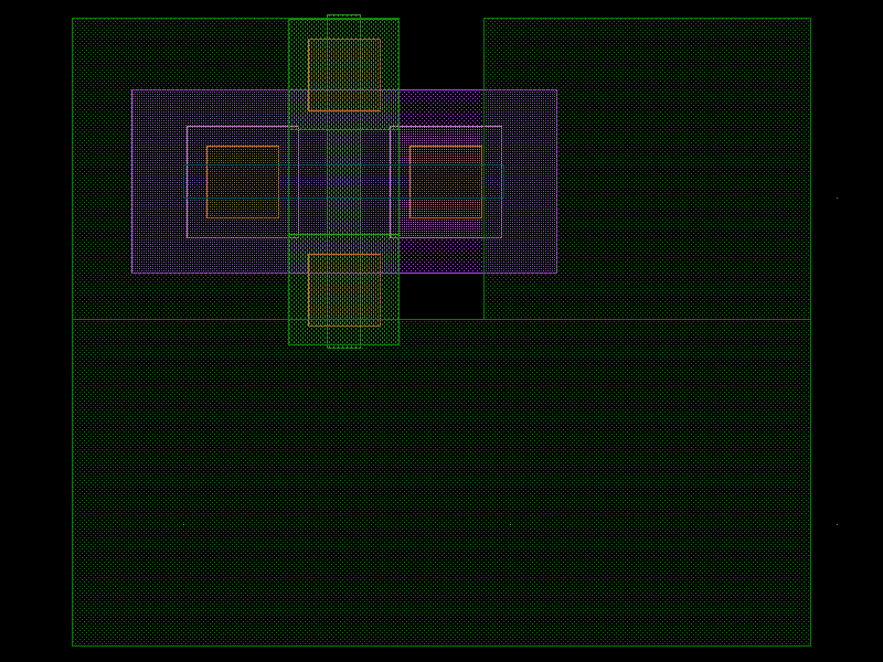
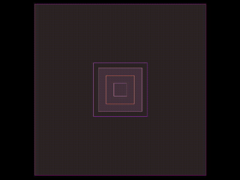
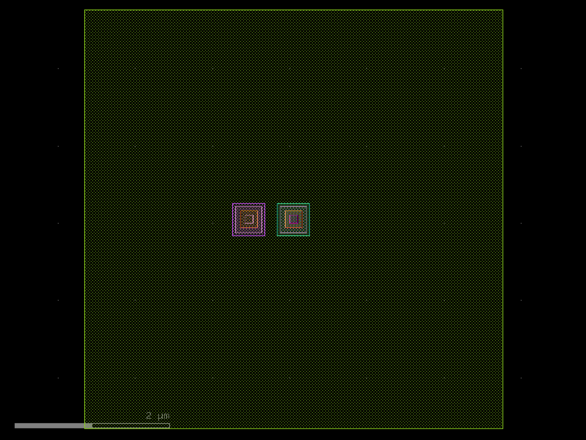
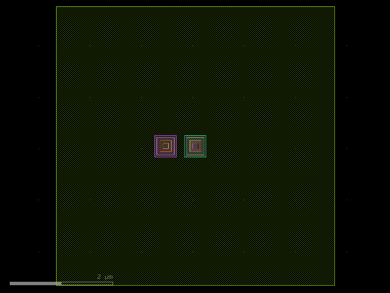
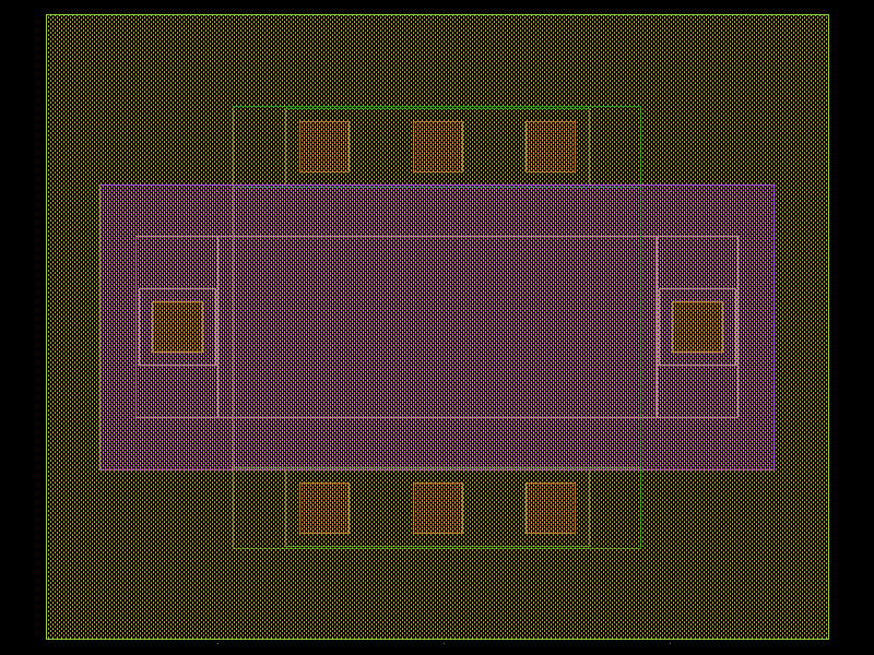
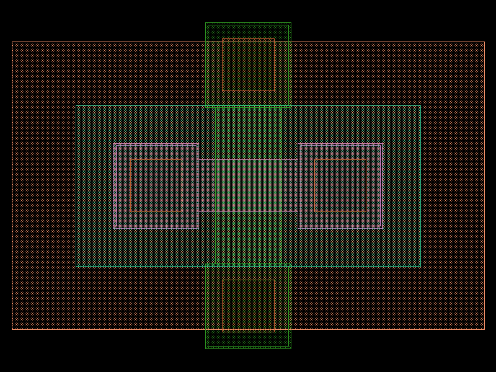
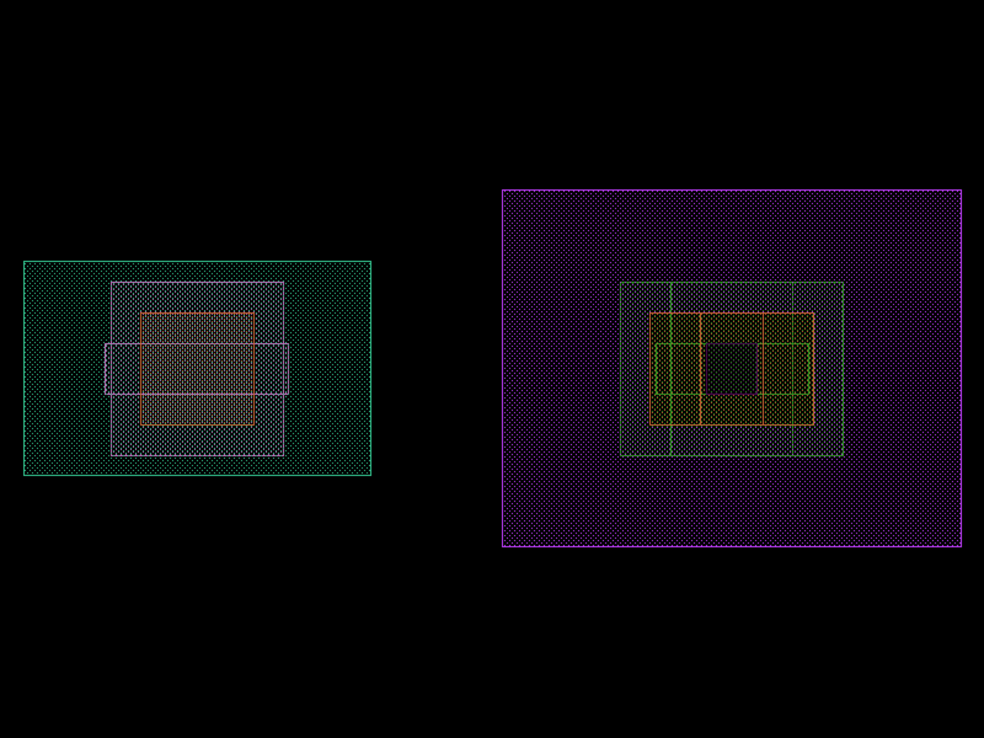
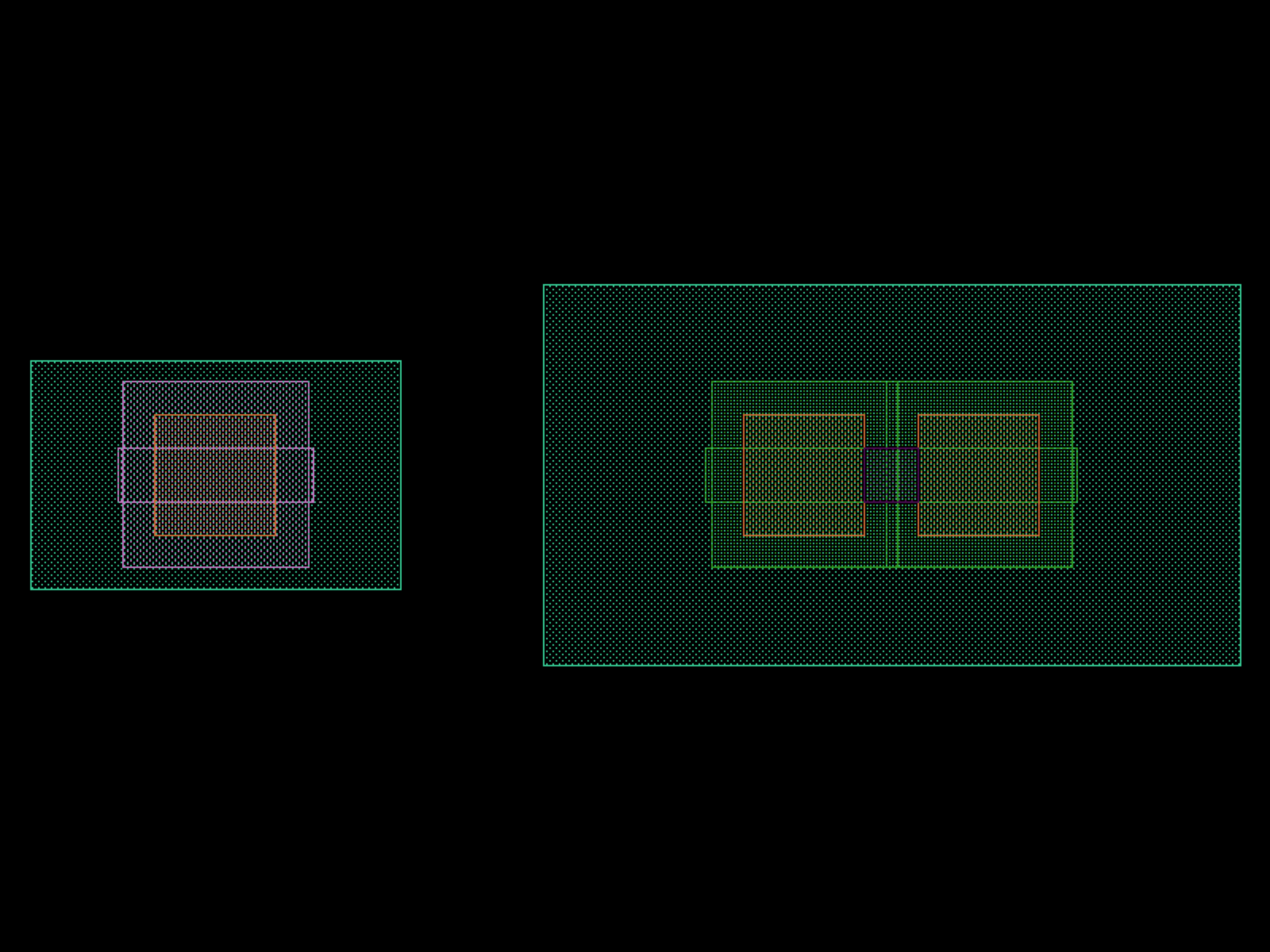
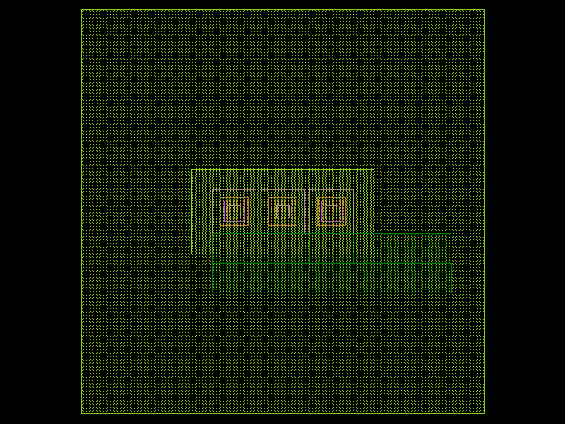
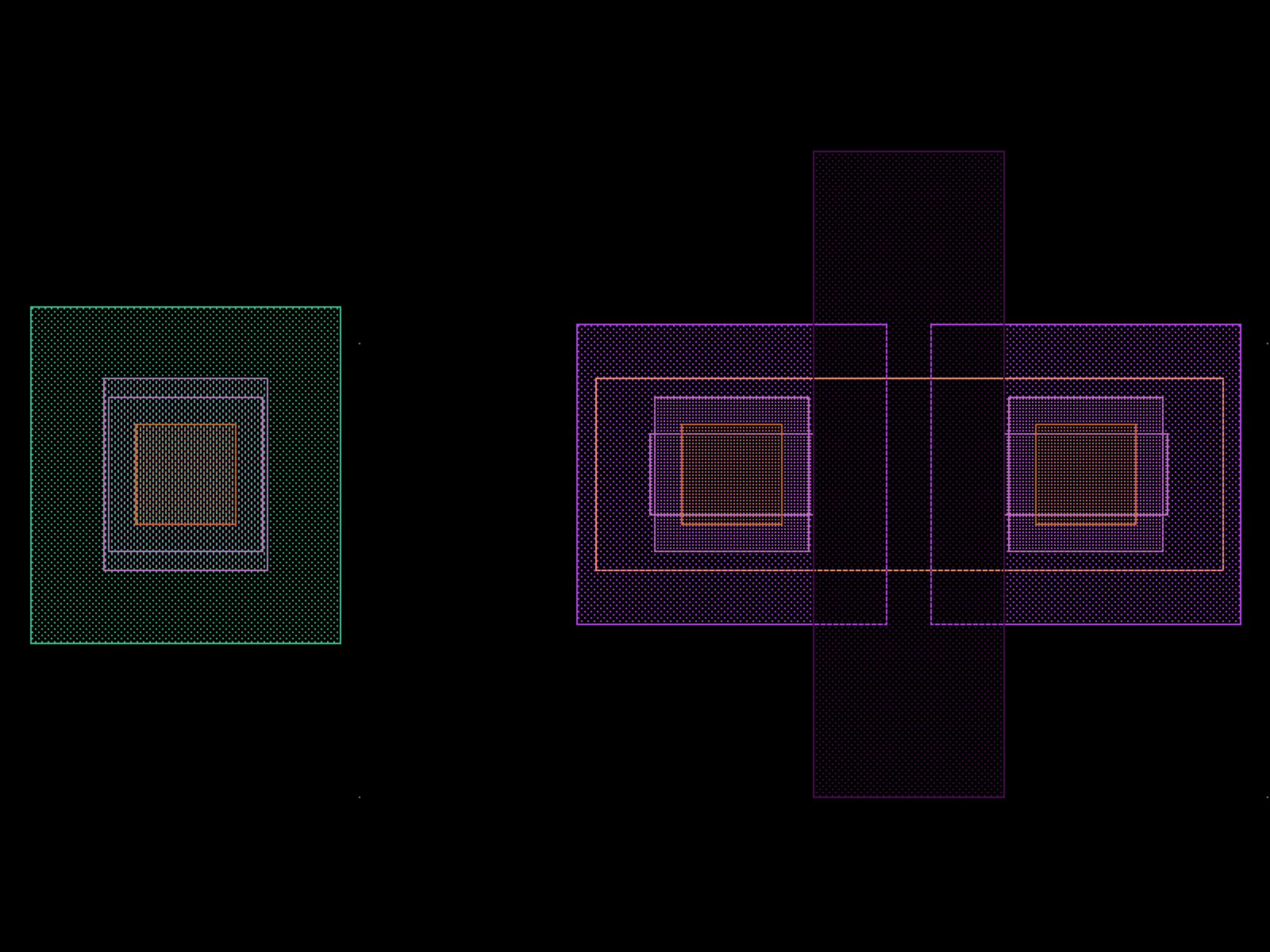
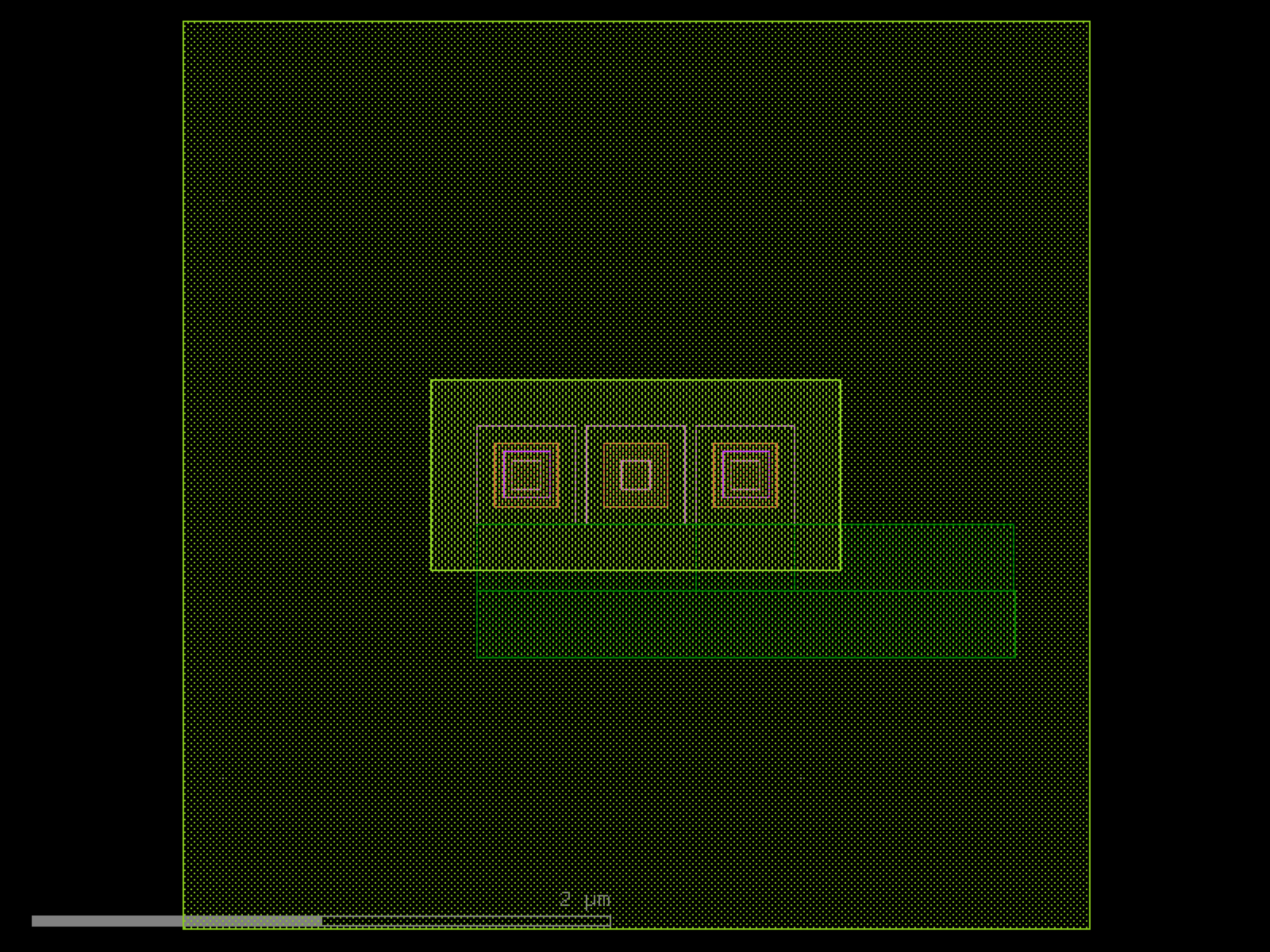
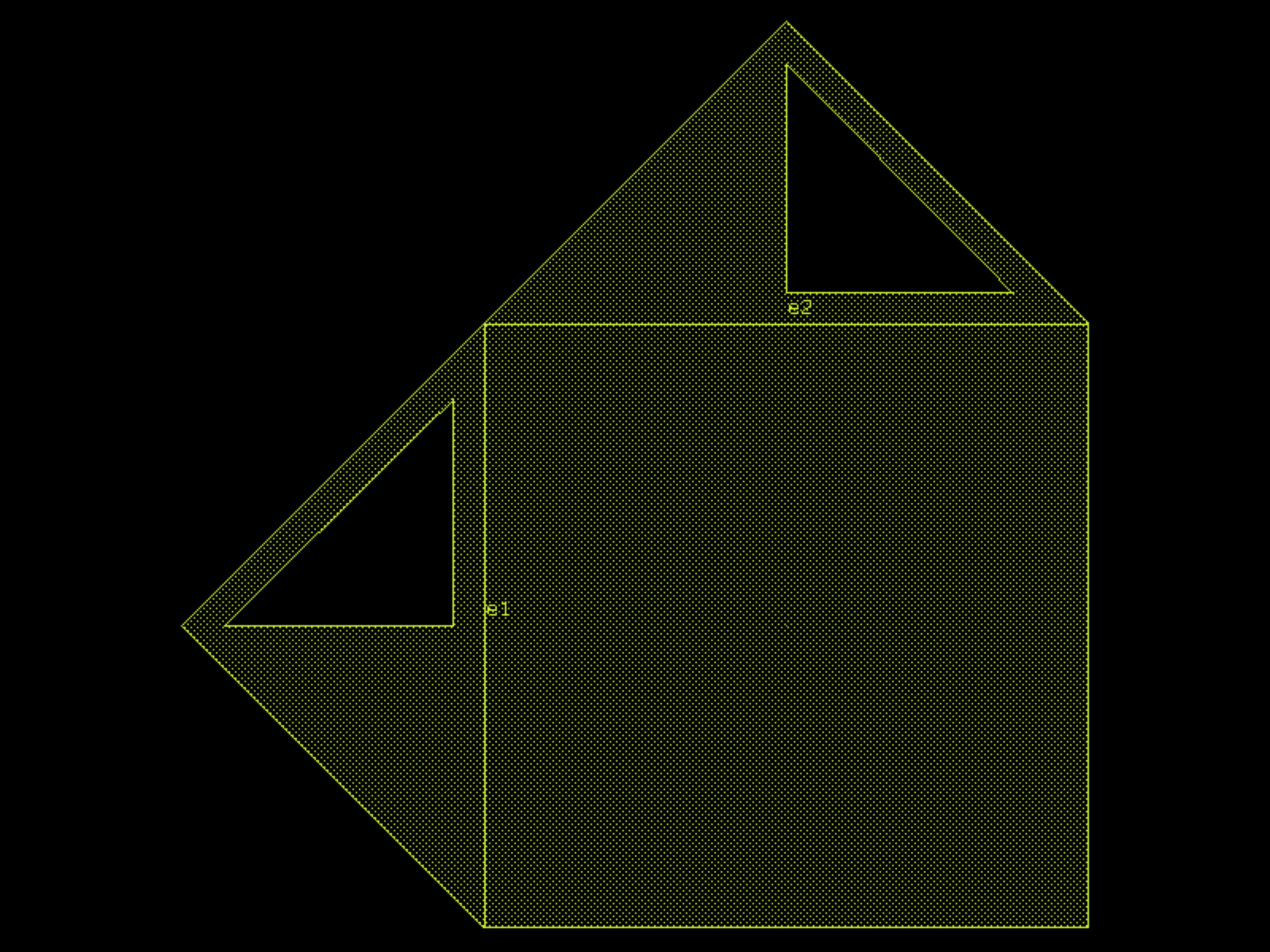
alter_interdig#
- gf180mcu.cells.alter_interdig(sd_diff=functools.partial(<function rectangle>, layer=<LAYER.comp: 14>), pc1=functools.partial(<function array>, component=functools.partial(<function rectangle>, layer=<LAYER.comp: 14>)), pc2=functools.partial(<function array>, component=functools.partial(<function rectangle>, layer=<LAYER.comp: 14>)), sd_l=0.36, nf=1, pat='', pc_x=0.1, pc_spacing=0.1, label=False, g_label=None, nl=1, patt_label=False)[source]#
Returns interdigitation polygons of gate with alternating poly contacts.
- Args :
sd_diff : source/drain diffusion rectangle. pc1 : first poly contact array. pc2 : second poly contact array. sd_l : source/drain length. nf : number of fingers. pat: string of the required pattern. poly_con : component of poly contact. sd_diff_inter : inter source/drain diffusion rectangle. l_gate : gate length. inter_sd_l : inter diffusion length. nf : number of fingers.
- Parameters:
label (bool)
g_label (Sequence[str] | None)
nl (int)
patt_label (bool)
- Return type:
Component
from gf180mcu import cells

c = cells.alter_interdig(sd_l=0.36, nf=1, pat='', pc_x=0.1, pc_spacing=0.1, label=False, nl=1, patt_label=False)
c = c.copy()
c.draw_ports()
c.plot()
(Source code, png, hires.png, pdf)

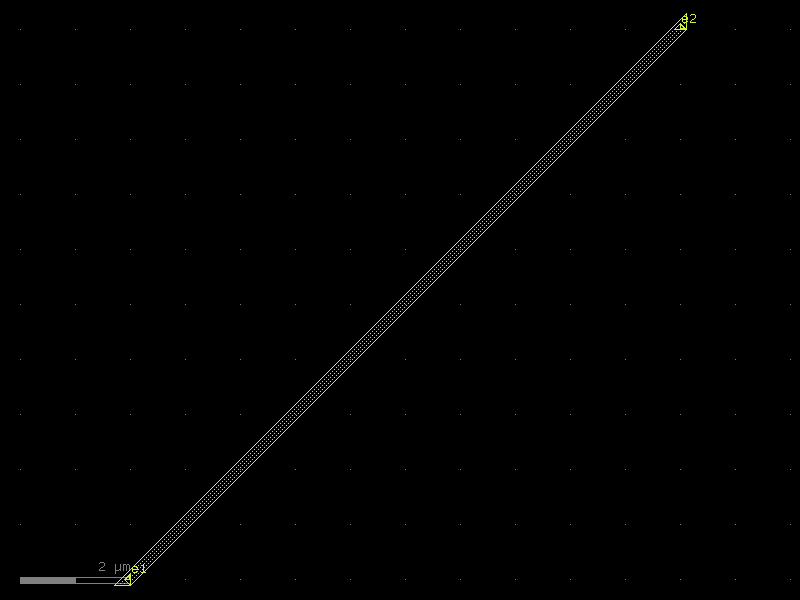
bend#
- gf180mcu.cells.bend(radius=None, angle=90, width=None, cross_section='metal1')[source]#
Regular degree euler bend.
- Parameters:
radius (float | None)
angle (float)
width (float | None)
cross_section (CrossSection | str | dict[str, Any] | Callable[[...], CrossSection] | SymmetricalCrossSection | DCrossSection)
- Return type:
Component
from gf180mcu import cells

c = cells.bend(angle=90, cross_section='metal1')
c = c.copy()
c.draw_ports()
c.plot()
(Source code, png, hires.png, pdf)
bend_s#
- gf180mcu.cells.bend_s(size=(11, 1.8), cross_section='metal1', width=None)[source]#
Return S bend with bezier curve.
stores min_bend_radius property in self.info[‘min_bend_radius’] min_bend_radius depends on height and length
- Parameters:
size (tuple[float, float]) – in x and y direction.
cross_section (CrossSection | str | dict[str, Any] | Callable[[...], CrossSection] | SymmetricalCrossSection | DCrossSection) – spec.
width (float | None) – width of the waveguide. If None, it will use the width of the cross_section.
- Return type:
Component
from gf180mcu import cells

c = cells.bend_s(size=(11, 1.8), cross_section='metal1')
c = c.copy()
c.draw_ports()
c.plot()
(Source code, png, hires.png, pdf)

cap_mim#
- gf180mcu.cells.cap_mim(mim_option='A', metal_level='M4', lc=2, wc=2, label=False, top_label='', bot_label='')[source]#
Return mim cap.
- Parameters:
min_option – MIM-A or MIM-B.
metal_level (str) – metal level. M4, M5, M6.
lc (float) – cap length.
wc (float) – cap width.
label (bool) – 1 to add labels.
top_label (str) – top label.
bot_label (str) – bottom label.
mim_option (str)
- Return type:
Component
from gf180mcu import cells

c = cells.cap_mim(mim_option='A', metal_level='M4', lc=2, wc=2, label=False, top_label='', bot_label='')
c = c.copy()
c.draw_ports()
c.plot()
(Source code, png, hires.png, pdf)
cap_mos#
- gf180mcu.cells.cap_mos(type='cap_nmos', lc=0.1, wc=0.1, volt='3.3V', deepnwell=False, pcmpgr=False, label=False, g_label='', sd_label='')[source]#
- Usage:-
used to draw NMOS capacitor (Outside DNWELL) by specifying parameters
- Arguments:-
l : Float of diff length w : Float of diff width.
- Parameters:
type (str)
lc (float)
wc (float)
volt (str)
deepnwell (bool)
pcmpgr (bool)
label (bool)
g_label (str)
sd_label (str)
- Return type:
Component
from gf180mcu import cells

c = cells.cap_mos(type='cap_nmos', lc=0.1, wc=0.1, volt='3.3V', deepnwell=False, pcmpgr=False, label=False, g_label='', sd_label='')
c = c.copy()
c.draw_ports()
c.plot()
(Source code, png, hires.png, pdf)

cap_mos_inst#
- gf180mcu.cells.cap_mos_inst(lc=0.1, wc=0.1, cmp_w=0.1, con_w=0.1, pl_l=0.1, cmp_ext=0.1, pl_ext=0.1, implant_layer=<LAYER.nplus: 49>, implant_enc=(0.1, 0.1), label=False, g_label='')[source]#
Returns mos cap simple instance.
- Parameters:
lc (float) – length of mos_cap.
ws – width of mos_cap.
cmp_w (float) – width of layer[“comp”].
con_w (float) – min width of comp contain contact.
pl_l (float) – length od layer[“poly2”].
cmp_ext (float) – comp extension beyond poly2.
pl_ext (float) – poly2 extension beyond comp.
implant_layer (tuple[int, int] | str | int | LayerEnum) – Layer of implant [nplus,pplus].
implant_enc (tuple[float, float]) – enclosure of implant_layer to comp.
label (bool) – 1 to add labels.
g_label (str) – gate label.
wc (float)
- Return type:
Component
from gf180mcu import cells

c = cells.cap_mos_inst(lc=0.1, wc=0.1, cmp_w=0.1, con_w=0.1, pl_l=0.1, cmp_ext=0.1, pl_ext=0.1, implant_layer='nplus', implant_enc=(0.1, 0.1), label=False, g_label='')
c = c.copy()
c.draw_ports()
c.plot()
(Source code, png, hires.png, pdf)

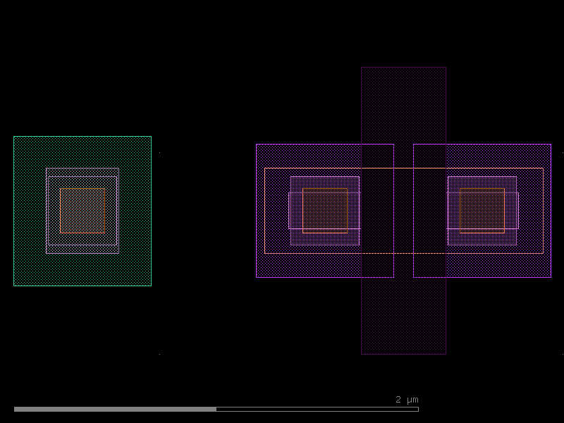
diode_dw2ps#
- gf180mcu.cells.diode_dw2ps(la=0.1, wa=0.1, cw=0.1, volt='3.3V', pcmpgr=False, label=False, p_label='', n_label='')[source]#
Used to draw LVPWELL/DNWELL diode by specifying parameters.
- Parameters:
la (float) – anode length.
wa (float) – anode width.
cw (float) – cathode width.
volt (str) – operating voltage of the diode [3.3V, 5V/6V].
pcmpgr (bool) – True if pwell guardring is required.
label (bool) – True if labels are required.
p_label (str) – label for pwell.
n_label (str) – label for nwell.
- Return type:
Component
from gf180mcu import cells

c = cells.diode_dw2ps(la=0.1, wa=0.1, cw=0.1, volt='3.3V', pcmpgr=False, label=False, p_label='', n_label='')
c = c.copy()
c.draw_ports()
c.plot()
(Source code, png, hires.png, pdf)

diode_nd2ps#
- gf180mcu.cells.diode_nd2ps(la=0.1, wa=0.1, cw=0.1, volt='3.3V', deepnwell=False, pcmpgr=False, label=False, p_label='', n_label='')[source]#
Draw N+/LVPWELL diode (Outside DNWELL) by specifying parameters.
- Args::
la: Float of diff length (anode). wa: Float of diff width (anode). cw: Float of cathode width. volt: String of operating voltage of the diode [3.3V, 5V/6V]. deepnwell: Boolean of using Deep NWELL device. pcmpgr : Boolean of using P+ Guard Ring for Deep NWELL devices only. label: Boolean of adding labels.
- Parameters:
la (float)
wa (float)
cw (float)
volt (str)
deepnwell (bool)
pcmpgr (bool)
label (bool)
p_label (str)
n_label (str)
- Return type:
Component
from gf180mcu import cells

c = cells.diode_nd2ps(la=0.1, wa=0.1, cw=0.1, volt='3.3V', deepnwell=False, pcmpgr=False, label=False, p_label='', n_label='')
c = c.copy()
c.draw_ports()
c.plot()
(Source code, png, hires.png, pdf)

diode_nw2ps#
- gf180mcu.cells.diode_nw2ps(la=0.1, wa=0.1, cw=0.1, volt='3.3V', label=False, p_label='', n_label='')[source]#
Used to draw 3.3V Nwell/Psub diode by specifying parameters.
- Parameters:
la (float) – anode length.
wa (float) – anode width.
cw (float) – cathode width.
volt (str) – operating voltage of the diode [3.3V, 5V/6V]
label (bool)
p_label (str)
n_label (str)
- Return type:
Component
from gf180mcu import cells

c = cells.diode_nw2ps(la=0.1, wa=0.1, cw=0.1, volt='3.3V', label=False, p_label='', n_label='')
c = c.copy()
c.draw_ports()
c.plot()
(Source code, png, hires.png, pdf)
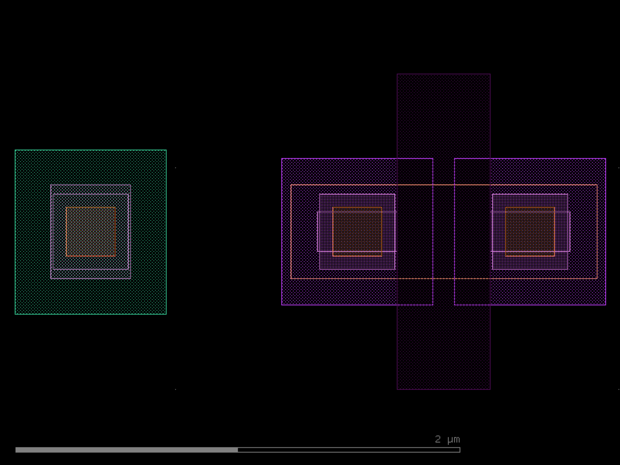
diode_pd2nw#
- gf180mcu.cells.diode_pd2nw(la=0.1, wa=0.1, cw=0.1, volt='3.3V', deepnwell=False, pcmpgr=False, label=False, p_label='', n_label='')[source]#
- Usage:-
used to draw 3.3V P+/Nwell diode (Outside DNWELL) by specifying parameters
- Arguments:-
la : Float of diffusion length (anode) wa : Float of diffusion width (anode) volt : String of operating voltage of the diode [3.3V, 5V/6V] deepnwell : Boolean of using Deep NWELL device pcmpgr : Boolean of using P+ Guard Ring for Deep NWELL devices only.
- Parameters:
la (float)
wa (float)
cw (float)
volt (str)
deepnwell (bool)
pcmpgr (bool)
label (bool)
p_label (str)
n_label (str)
- Return type:
Component
from gf180mcu import cells

c = cells.diode_pd2nw(la=0.1, wa=0.1, cw=0.1, volt='3.3V', deepnwell=False, pcmpgr=False, label=False, p_label='', n_label='')
c = c.copy()
c.draw_ports()
c.plot()
(Source code, png, hires.png, pdf)

diode_pw2dw#
- gf180mcu.cells.diode_pw2dw(la=0.1, wa=0.1, cw=0.1, volt='3.3V', pcmpgr=False, label=False, p_label='', n_label='')[source]#
Used to draw LVPWELL/DNWELL diode by specifying parameters.
- Parameters:
la (float) – anode length.
wa (float) – anode width.
cw (float) – cathode width.
volt (str) – operating voltage of the diode [3.3V, 5V/6V]
pcmpgr (bool) – if True, pcmpgr will be added.
label (bool) – if True, labels will be added.
p_label (str) – p contact label.
n_label (str) – n contact label.
- Return type:
Component
from gf180mcu import cells

c = cells.diode_pw2dw(la=0.1, wa=0.1, cw=0.1, volt='3.3V', pcmpgr=False, label=False, p_label='', n_label='')
c = c.copy()
c.draw_ports()
c.plot()
(Source code, png, hires.png, pdf)
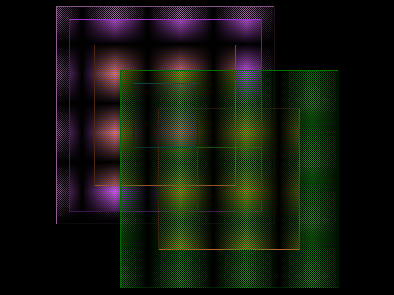
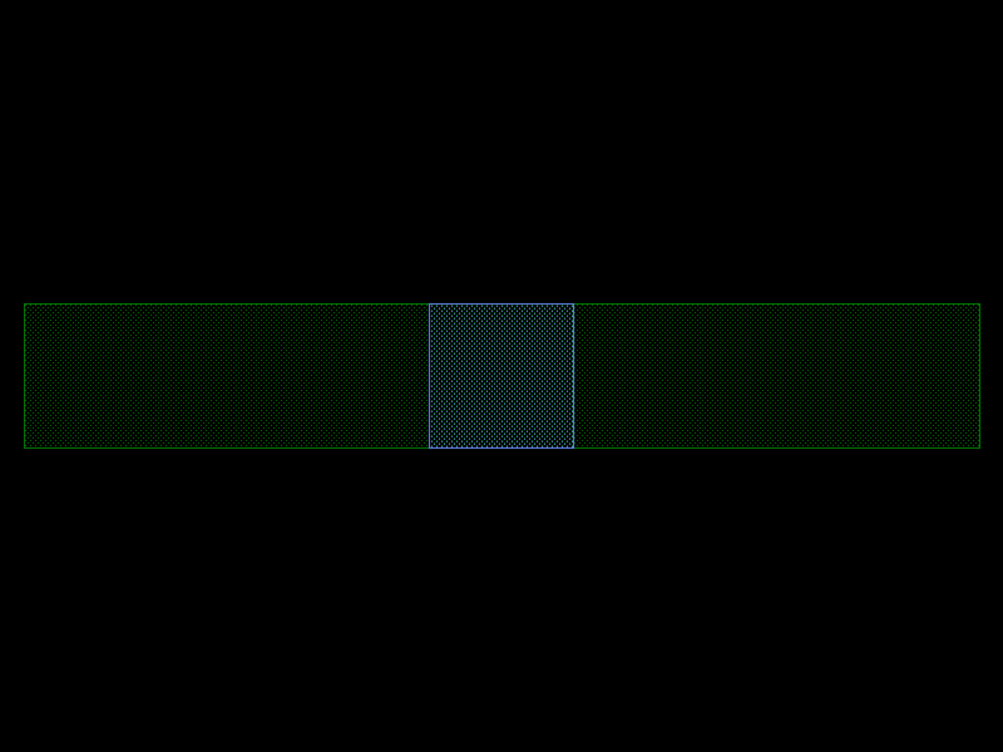
dn_rect#
- gf180mcu.cells.dn_rect(size=(4.0, 2.0), *, layer=<LAYER.dnwell: 46>, centered=False, port_type='electrical', port_orientations=(180, 90, 0, -90))#
Returns a rectangle.
- Parameters:
size (Size) – (tuple) Width and height of rectangle.
layer (LayerSpec) – Specific layer to put polygon geometry on.
centered (bool) – True sets center to (0, 0), False sets south-west to (0, 0).
port_type (str | None) – optical, electrical.
port_orientations (Ints | None) – list of port_orientations to add. None adds no ports.
- Return type:
Component
from gf180mcu import cells

c = cells.dn_rect(size=(4, 2), layer='dnwell', centered=False, port_type='electrical', port_orientations=(180, 90, 0, -90))
c = c.copy()
c.draw_ports()
c.plot()
(Source code, png, hires.png, pdf)

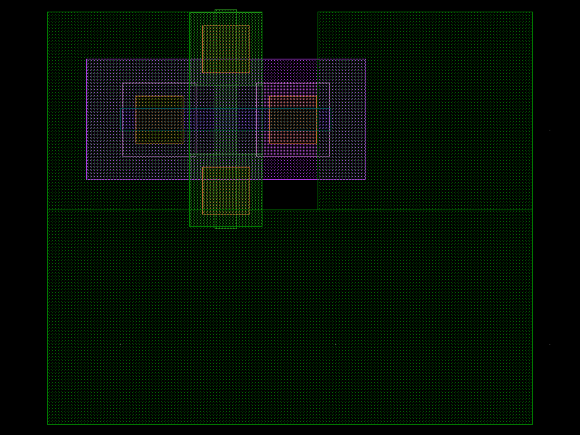
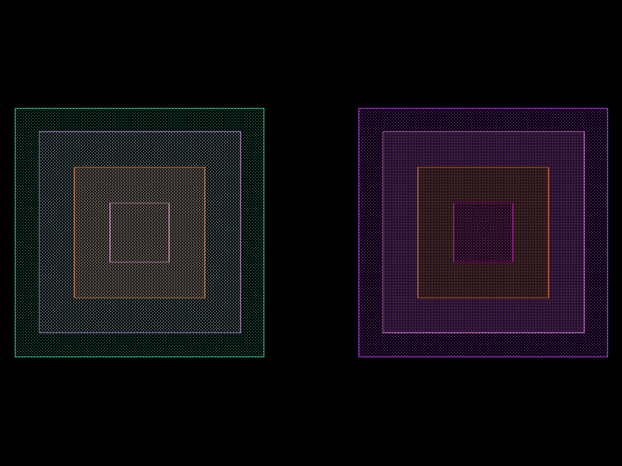
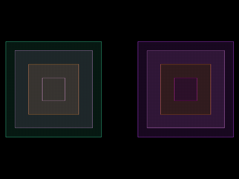
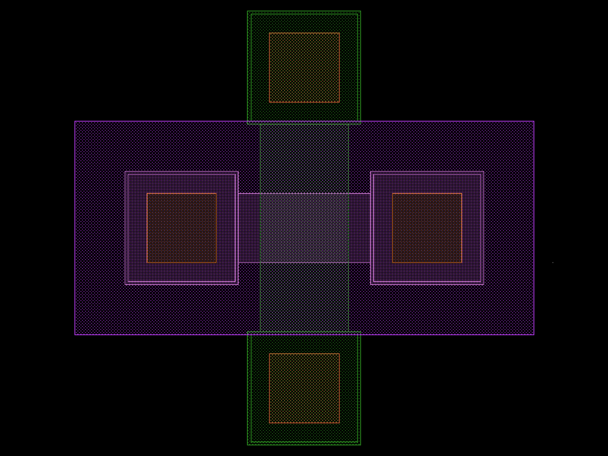
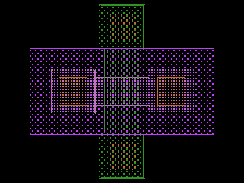
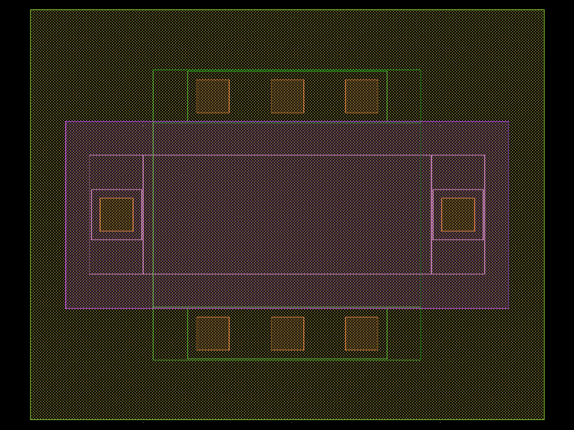
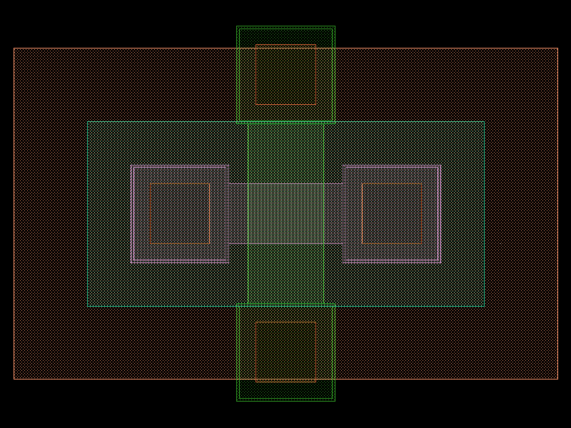
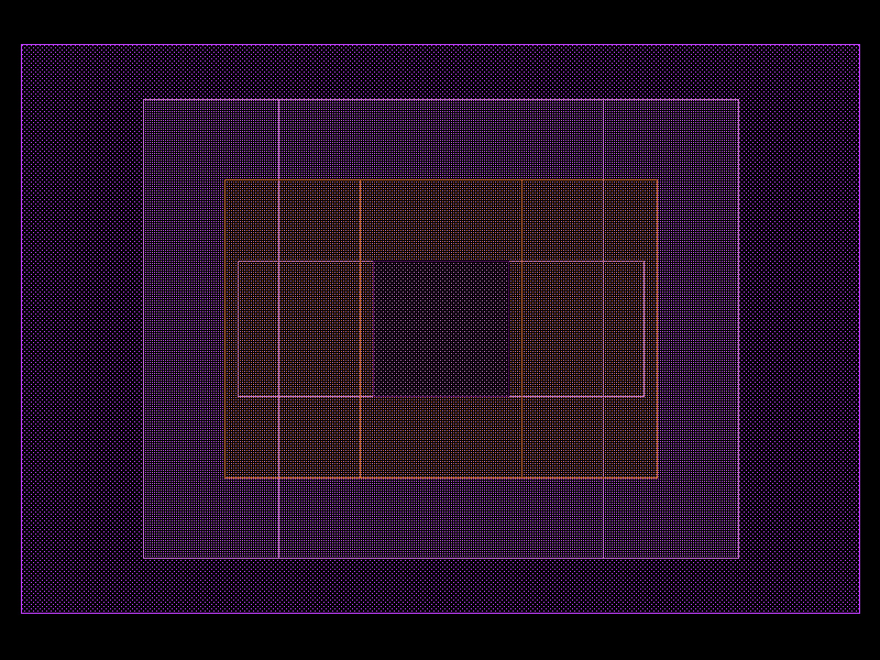
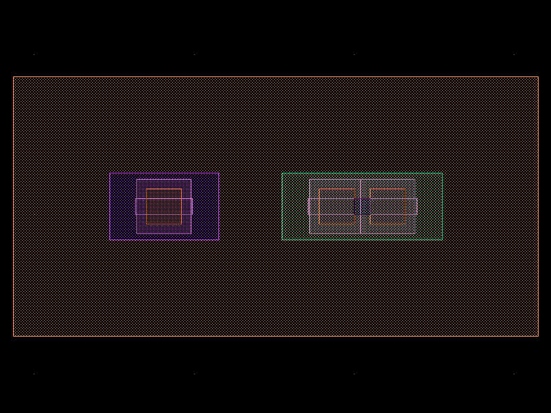
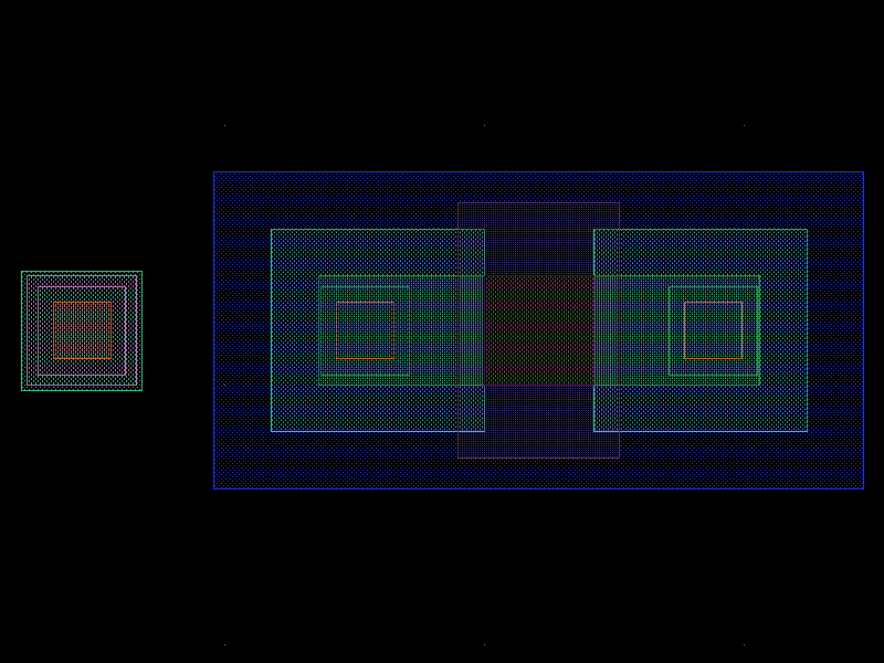
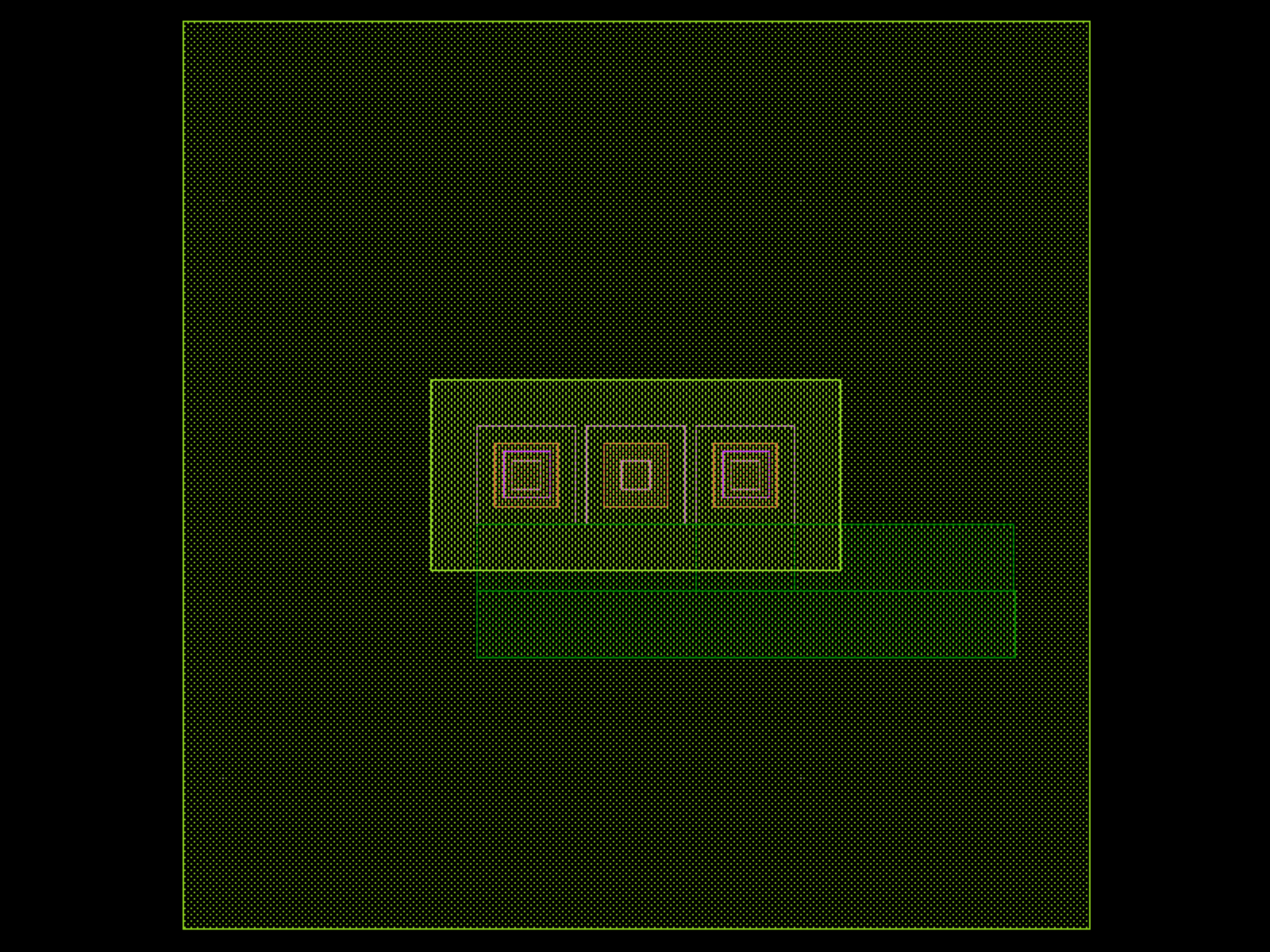
interdigit#
- gf180mcu.cells.interdigit(sd_diff=functools.partial(<function rectangle>, layer=<LAYER.comp: 14>), pc1=functools.partial(<function array>, component=functools.partial(<function rectangle>, layer=<LAYER.comp: 14>)), pc2=functools.partial(<function array>, component=functools.partial(<function rectangle>, layer=<LAYER.comp: 14>)), poly_con=functools.partial(<function rectangle>, layer=<LAYER.comp: 14>), sd_l=0.15, nf=1, patt=[''], gate_con_pos='top', pc_x=0.1, pc_spacing=0.1, label=False, g_label=None, patt_label=False)[source]#
Returns interdigitation related polygons.
- Args :
sd_diff : source/drain diffusion rectangle. pc1: first poly contact array. pc2: second poly contact array. poly_con: poly contact. sd_diff_inter : inter source/drain diffusion rectangle. l_gate : gate length. inter_sd_l : inter diffusion length. nf : number of fingers. pat : string of the required pattern. gate_con_pos : position of gate contact.
- Parameters:
sd_l (float)
label (bool)
g_label (Sequence[str] | None)
patt_label (bool)
- Return type:
Component
from gf180mcu import cells

c = cells.interdigit(sd_l=0.15, nf=1, gate_con_pos='top', pc_x=0.1, pc_spacing=0.1, label=False, patt_label=False)
c = c.copy()
c.draw_ports()
c.plot()
(Source code, png, hires.png, pdf)

labels_gen#
- gf180mcu.cells.labels_gen(label_str='', position=(0.1, 0.1), layer=<LAYER.metal1_label: 76>, label=False, labels=None, label_valid_len=1, index=0)[source]#
Returns labels at given position when label is enabled.
- Args :
label_str : string of the label. position : position of the label. layer : layer of the label. label : boolean of having the label. labels : list of given labels. label_valid_len : valid length of labels.
- Parameters:
label_str (str)
position (tuple[float, float])
layer (tuple[int, int] | str | int | LayerEnum)
label (bool)
labels (Sequence[str] | None)
label_valid_len (int)
index (int)
- Return type:
Component
from gf180mcu import cells

c = cells.labels_gen(label_str='', position=(0.1, 0.1), layer='metal1_label', label=False, label_valid_len=1, index=0)
c = c.copy()
c.draw_ports()
c.plot()
(Source code, png, hires.png, pdf)
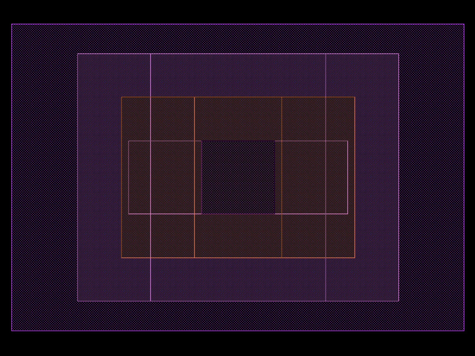
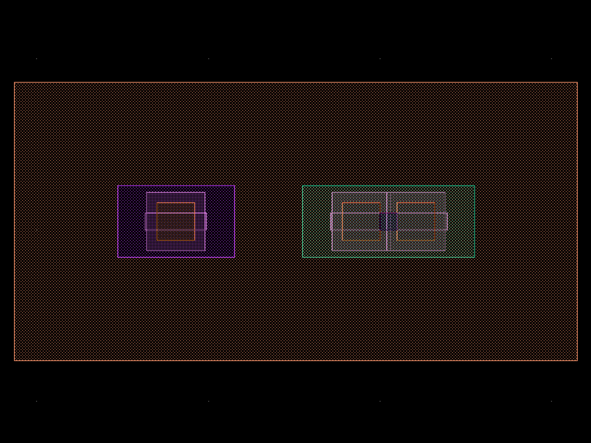
nfet#
- gf180mcu.cells.nfet(l_gate=0.28, w_gate=0.22, sd_con_col=1, inter_sd_l=0.24, nf=1, grw=0.22, volt='3.3V', bulk='None', con_bet_fin=1, gate_con_pos='alternating', interdig=0, patt='', deepnwell=0, pcmpgr=0, label=False, sd_label=[], g_label=(), sub_label='', patt_label=False)[source]#
Return nfet.
- Parameters:
l – Float of gate length
w – Float of gate width
sd_l – Float of source and drain diffusion length
inter_sd_l (float) – Float of source and drain diffusion length between fingers
nf (int) – integer of number of fingers
M – integer of number of multipliers
grw (float) – guard ring width when enabled
type – string of the device type
bulk (str) – String of bulk connection type (None, Bulk Tie, Guard Ring)
con_bet_fin (int) – boolean of having contacts for diffusion between fingers
gate_con_pos (str) – string of choosing the gate contact position (bottom, top, alternating )
l_gate (float)
w_gate (float)
sd_con_col (int)
volt (str)
interdig (int)
patt (str)
deepnwell (int)
pcmpgr (int)
label (bool)
sd_label (Sequence[str] | None)
g_label (Sequence[str])
sub_label (str)
patt_label (bool)
- Return type:
Component
from gf180mcu import cells

c = cells.nfet(l_gate=0.28, w_gate=0.22, sd_con_col=1, inter_sd_l=0.24, nf=1, grw=0.22, volt='3.3V', bulk='None', con_bet_fin=1, gate_con_pos='alternating', interdig=0, patt='', deepnwell=0, pcmpgr=0, label=False, g_label=(), sub_label='', patt_label=False)
c = c.copy()
c.draw_ports()
c.plot()
(Source code, png, hires.png, pdf)

nfet_06v0_nvt#
- gf180mcu.cells.nfet_06v0_nvt(l_gate=1.8, w_gate=0.8, sd_con_col=1, inter_sd_l=0.24, nf=1, grw=0.22, bulk='None', con_bet_fin=1, gate_con_pos='alternating', interdig=0, patt='', label=False, sd_label=[], g_label=[], sub_label='', patt_label=False)[source]#
Draw Native NFET 6V transistor by specifying parameters.
- Arg:
l : Float of gate length w : Float of gate width ld : Float of diffusion length nf : Integer of number of fingers grw : Float of guard ring width [If enabled] bulk : String of bulk connection type [None, Bulk Tie, Guard Ring]
- Parameters:
l_gate (float)
w_gate (float)
sd_con_col (int)
inter_sd_l (float)
nf (int)
grw (float)
con_bet_fin (int)
interdig (int)
label (bool)
sd_label (Sequence[str] | None)
g_label (str)
sub_label (str)
patt_label (bool)
- Return type:
Component
from gf180mcu import cells

c = cells.nfet_06v0_nvt(l_gate=1.8, w_gate=0.8, sd_con_col=1, inter_sd_l=0.24, nf=1, grw=0.22, bulk='None', con_bet_fin=1, gate_con_pos='alternating', interdig=0, patt='', label=False, sub_label='', patt_label=False)
c = c.copy()
c.draw_ports()
c.plot()
(Source code, png, hires.png, pdf)

nfet_deep_nwell#
- gf180mcu.cells.nfet_deep_nwell(deepnwell=False, pcmpgr=False, inst_size=(0.1, 0.1), inst_xmin=0.1, inst_ymin=0.1, grw=0.36)[source]#
Return nfet deepnwell.
- Args :
deepnwell : boolean of having deepnwell pcmpgr : boolean of having deepnwell guardring inst_size : deepnwell enclosed size inst_xmin : deepnwell enclosed dxmin inst_ymin : deepnwell enclosed dymin grw : guardring width
- Parameters:
deepnwell (bool)
pcmpgr (bool)
inst_size (tuple[float, float])
inst_xmin (float)
inst_ymin (float)
grw (float)
- Return type:
Component
from gf180mcu import cells

c = cells.nfet_deep_nwell(deepnwell=False, pcmpgr=False, inst_size=(0.1, 0.1), inst_xmin=0.1, inst_ymin=0.1, grw=0.36)
c = c.copy()
c.draw_ports()
c.plot()
(Source code, png, hires.png, pdf)

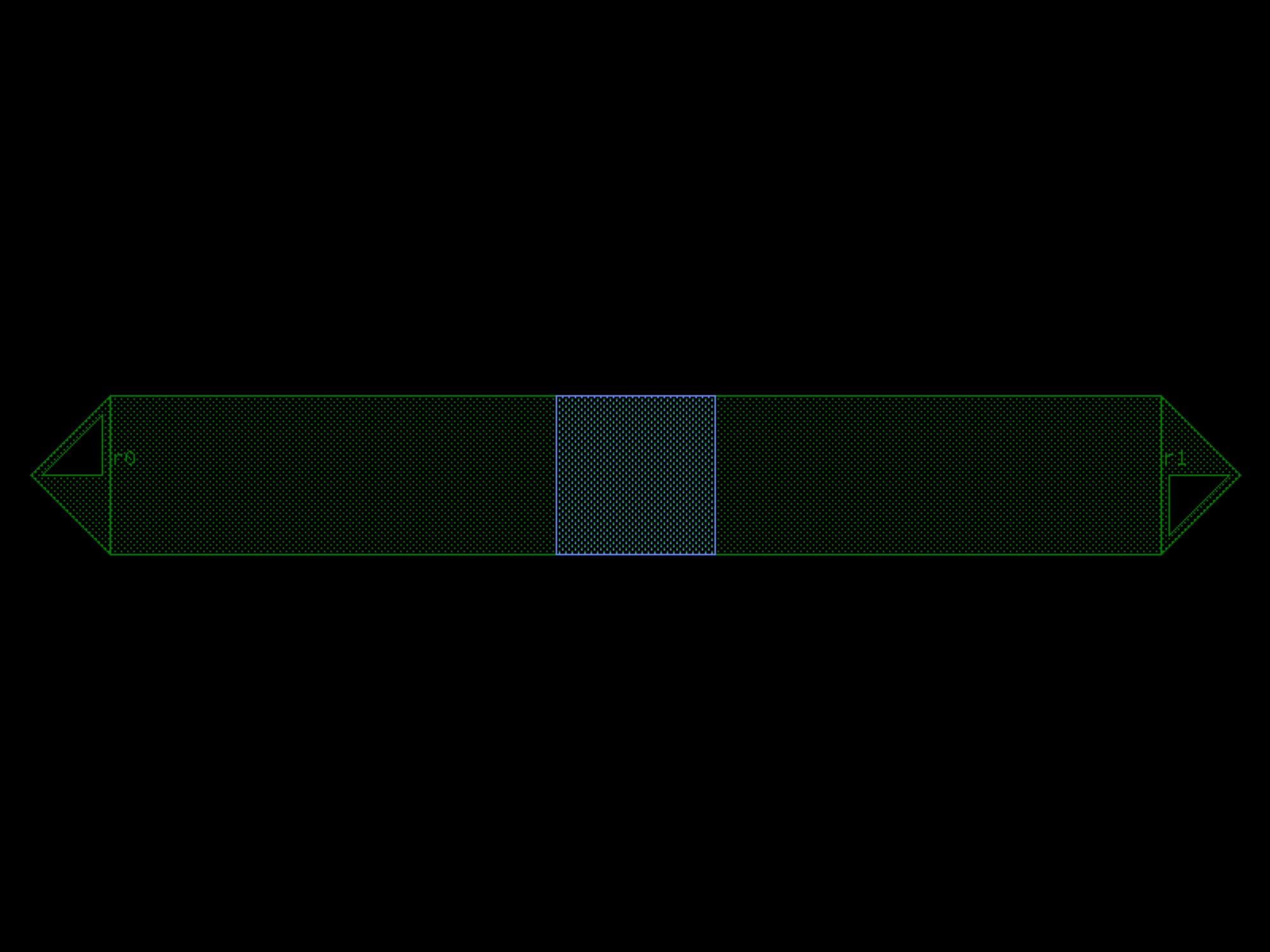
nplus_res#
- gf180mcu.cells.nplus_res(l_res=0.1, w_res=0.1, res_type='nplus_s', sub=False, deepnwell=False, pcmpgr=False, label=False, r0_label='', r1_label='', sub_label='')[source]#
- Parameters:
l_res (float)
w_res (float)
res_type (str)
sub (bool)
deepnwell (bool)
pcmpgr (bool)
label (bool)
r0_label (str)
r1_label (str)
sub_label (str)
- Return type:
Component
from gf180mcu import cells

c = cells.nplus_res(l_res=0.1, w_res=0.1, res_type='nplus_s', sub=False, deepnwell=False, pcmpgr=False, label=False, r0_label='', r1_label='', sub_label='')
c = c.copy()
c.draw_ports()
c.plot()
(Source code, png, hires.png, pdf)

npolyf_res#
- gf180mcu.cells.npolyf_res(l_res=0.1, w_res=0.1, res_type='npolyf_s', deepnwell=False, pcmpgr=False, label=False, r0_label='', r1_label='', sub_label='')[source]#
- Parameters:
l_res (float)
w_res (float)
res_type (str)
deepnwell (bool)
pcmpgr (bool)
label (bool)
r0_label (str)
r1_label (str)
sub_label (str)
- Return type:
Component
from gf180mcu import cells

c = cells.npolyf_res(l_res=0.1, w_res=0.1, res_type='npolyf_s', deepnwell=False, pcmpgr=False, label=False, r0_label='', r1_label='', sub_label='')
c = c.copy()
c.draw_ports()
c.plot()
(Source code, png, hires.png, pdf)

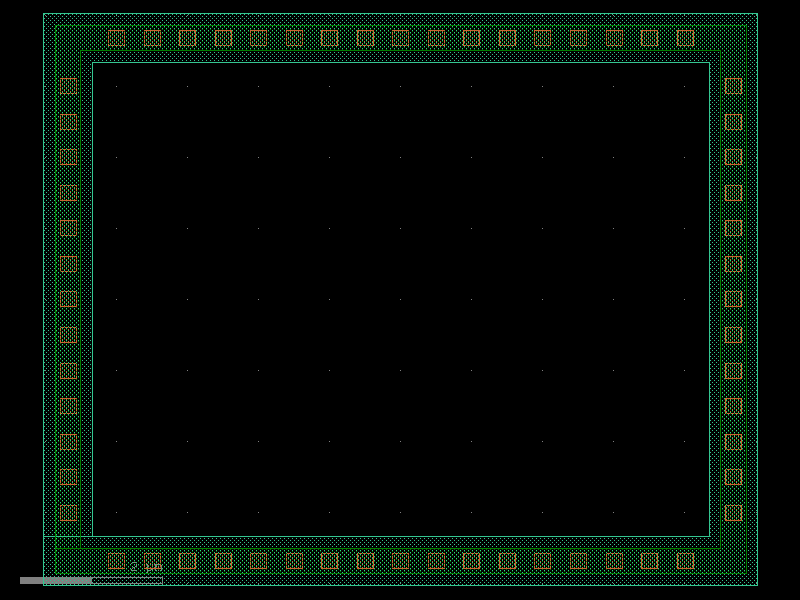
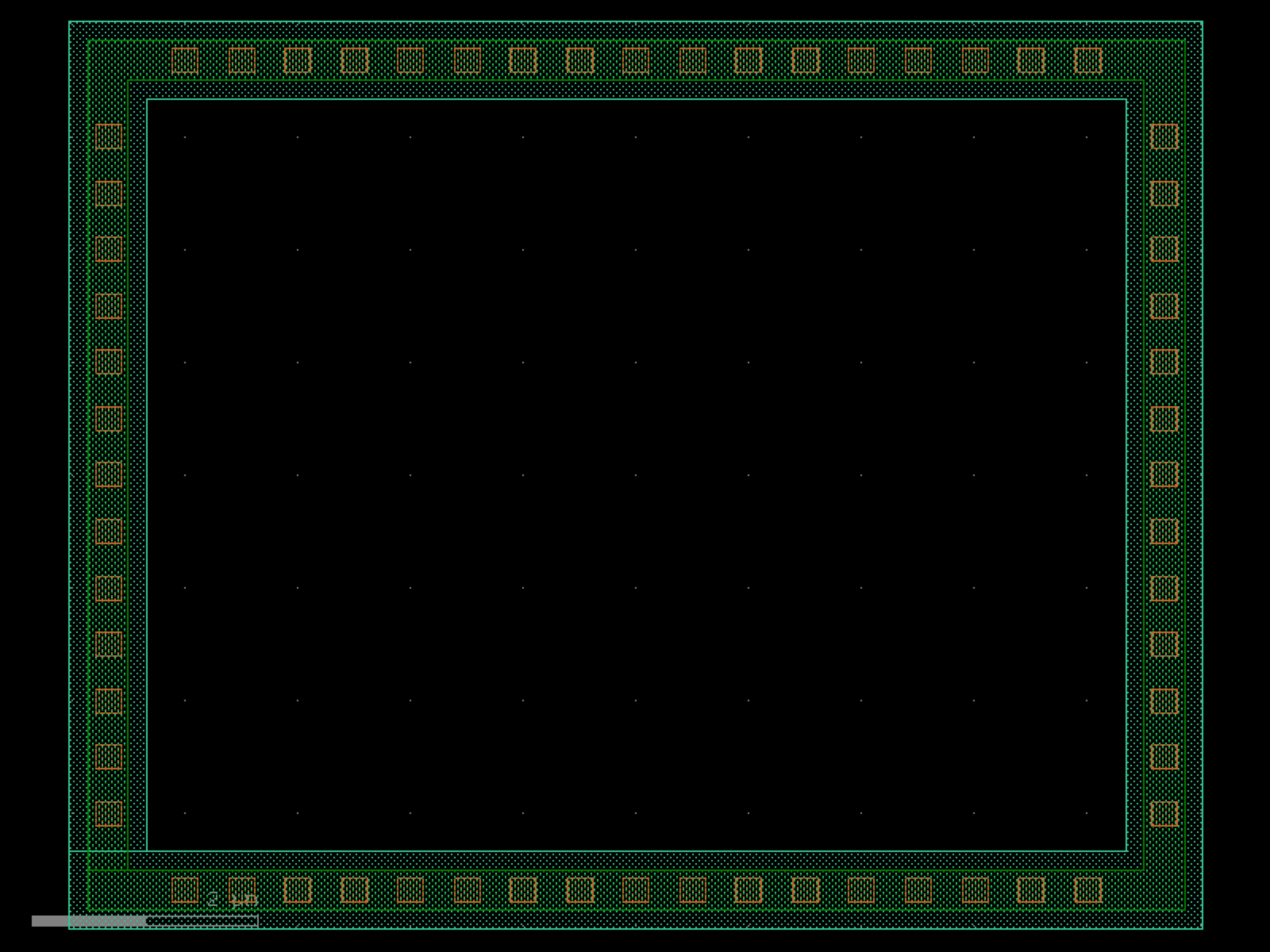
pcmpgr_gen#
- gf180mcu.cells.pcmpgr_gen(dn_rect=functools.partial(<function rectangle>, layer=<LAYER.dnwell: 46>), grw=0.36)[source]#
Return deepnwell guardring.
- Parameters:
dn_rect – deepnwell polygon.
grw (float) – guardring width.
- Return type:
Component
from gf180mcu import cells

c = cells.pcmpgr_gen(grw=0.36)
c = c.copy()
c.draw_ports()
c.plot()
(Source code, png, hires.png, pdf)

pfet#
- gf180mcu.cells.pfet(l_gate=0.28, w_gate=0.22, sd_con_col=1, inter_sd_l=0.24, nf=1, grw=0.22, volt='3.3V', bulk='None', con_bet_fin=1, gate_con_pos='alternating', interdig=0, patt='', deepnwell=0, pcmpgr=0, label=False, sd_label=(), g_label=(), sub_label='', patt_label=False)[source]#
Return pfet.
- Parameters:
l – Float of gate length
w – Float of gate width
sd_l – Float of source and drain diffusion length
inter_sd_l (float) – Float of source and drain diffusion length between fingers
nf (int) – integer of number of fingers
M – integer of number of multipliers
grw (float) – guard ring width when enabled
type – string of the device type
bulk (str) – String of bulk connection type (None, Bulk Tie, Guard Ring)
con_bet_fin (int) – boolean of having contacts for diffusion between fingers
gate_con_pos (str) – string of choosing the gate contact position (bottom, top, alternating )
l_gate (float)
w_gate (float)
sd_con_col (int)
volt (str)
interdig (int)
patt (str)
deepnwell (int)
pcmpgr (int)
label (bool)
sd_label (Sequence[str] | None)
g_label (Sequence[str])
sub_label (str)
patt_label (bool)
- Return type:
Component
from gf180mcu import cells

c = cells.pfet(l_gate=0.28, w_gate=0.22, sd_con_col=1, inter_sd_l=0.24, nf=1, grw=0.22, volt='3.3V', bulk='None', con_bet_fin=1, gate_con_pos='alternating', interdig=0, patt='', deepnwell=0, pcmpgr=0, label=False, sd_label=(), g_label=(), sub_label='', patt_label=False)
c = c.copy()
c.draw_ports()
c.plot()
(Source code, png, hires.png, pdf)

pfet_deep_nwell#
- gf180mcu.cells.pfet_deep_nwell(deepnwell=False, pcmpgr=False, enc_size=(0.1, 0.1), enc_xmin=0.1, enc_ymin=0.1, nw_enc_pcmp=0.1, grw=0.36)[source]#
Returns pfet well related polygons.
- Args :
deepnwell : boolaen of having deepnwell pcmpgr : boolean of having deepnwell guardring enc_size : enclosed size enc_xmin : enclosed dxmin enc_ymin : enclosed dymin nw_enc_pcmp : nwell enclosure of pcomp grw : guardring width
- Parameters:
deepnwell (bool)
pcmpgr (bool)
enc_size (tuple[float, float])
enc_xmin (float)
enc_ymin (float)
nw_enc_pcmp (float)
grw (float)
- Return type:
Component
from gf180mcu import cells

c = cells.pfet_deep_nwell(deepnwell=False, pcmpgr=False, enc_size=(0.1, 0.1), enc_xmin=0.1, enc_ymin=0.1, nw_enc_pcmp=0.1, grw=0.36)
c = c.copy()
c.draw_ports()
c.plot()
(Source code, png, hires.png, pdf)

plus_res_inst#
- gf180mcu.cells.plus_res_inst(l_res=0.1, w_res=0.1, res_type='nplus_s', sub=False, cmp_res_ext=0.1, con_enc=0.1, cmp_imp_layer=<LAYER.nplus: 49>, sub_imp_layer=<LAYER.pplus: 50>, label=False, r0_label='', r1_label='', sub_label='')[source]#
Returns 2-terminal Metal resistor by specifying parameters.
- Parameters:
l_res (float)
w_res (float)
res_type (str)
sub (bool)
cmp_res_ext (float)
con_enc (float)
cmp_imp_layer (tuple[int, int] | str | int | LayerEnum)
sub_imp_layer (tuple[int, int] | str | int | LayerEnum)
label (bool)
r0_label (str)
r1_label (str)
sub_label (str)
- Return type:
Component
from gf180mcu import cells

c = cells.plus_res_inst(l_res=0.1, w_res=0.1, res_type='nplus_s', sub=False, cmp_res_ext=0.1, con_enc=0.1, cmp_imp_layer='nplus', sub_imp_layer='pplus', label=False, r0_label='', r1_label='', sub_label='')
c = c.copy()
c.draw_ports()
c.plot()
(Source code, png, hires.png, pdf)
polyf_res_inst#
- gf180mcu.cells.polyf_res_inst(l_res=0.1, w_res=0.1, res_type='npolyf_s', pl_res_ext=0.1, con_enc=0.1, pl_imp_layer=<LAYER.nplus: 49>, sub_imp_layer=<LAYER.pplus: 50>, label=False, r0_label='', r1_label='', sub_label='')[source]#
- Parameters:
l_res (float)
w_res (float)
res_type (str)
pl_res_ext (float)
con_enc (float)
pl_imp_layer (tuple[int, int] | str | int | LayerEnum)
sub_imp_layer (tuple[int, int] | str | int | LayerEnum)
label (bool)
r0_label (str)
r1_label (str)
sub_label (str)
- Return type:
Component
from gf180mcu import cells

c = cells.polyf_res_inst(l_res=0.1, w_res=0.1, res_type='npolyf_s', pl_res_ext=0.1, con_enc=0.1, pl_imp_layer='nplus', sub_imp_layer='pplus', label=False, r0_label='', r1_label='', sub_label='')
c = c.copy()
c.draw_ports()
c.plot()
(Source code, png, hires.png, pdf)
pplus_res#
- gf180mcu.cells.pplus_res(l_res=0.1, w_res=0.1, res_type='pplus_s', sub=False, deepnwell=False, pcmpgr=False, label=False, r0_label='', r1_label='', sub_label='')[source]#
- Parameters:
l_res (float)
w_res (float)
res_type (str)
sub (bool)
deepnwell (bool)
pcmpgr (bool)
label (bool)
r0_label (str)
r1_label (str)
sub_label (str)
- Return type:
Component
from gf180mcu import cells

c = cells.pplus_res(l_res=0.1, w_res=0.1, res_type='pplus_s', sub=False, deepnwell=False, pcmpgr=False, label=False, r0_label='', r1_label='', sub_label='')
c = c.copy()
c.draw_ports()
c.plot()
(Source code, png, hires.png, pdf)

ppolyf_res#
- gf180mcu.cells.ppolyf_res(l_res=0.1, w_res=0.1, res_type='ppolyf_s', deepnwell=False, pcmpgr=False, label=False, r0_label='', r1_label='', sub_label='')[source]#
- Parameters:
l_res (float)
w_res (float)
res_type (str)
deepnwell (bool)
pcmpgr (bool)
label (bool)
r0_label (str)
r1_label (str)
sub_label (str)
- Return type:
Component
from gf180mcu import cells

c = cells.ppolyf_res(l_res=0.1, w_res=0.1, res_type='ppolyf_s', deepnwell=False, pcmpgr=False, label=False, r0_label='', r1_label='', sub_label='')
c = c.copy()
c.draw_ports()
c.plot()
(Source code, png, hires.png, pdf)

ppolyf_u_high_Rs_res#
- gf180mcu.cells.ppolyf_u_high_Rs_res(l_res=0.42, w_res=0.42, volt='3.3V', deepnwell=False, pcmpgr=False, label=False, r0_label='', r1_label='', sub_label='')[source]#
- Parameters:
l_res (float)
w_res (float)
volt (str)
deepnwell (bool)
pcmpgr (bool)
label (bool)
r0_label (str)
r1_label (str)
sub_label (str)
- Return type:
Component
from gf180mcu import cells

c = cells.ppolyf_u_high_Rs_res(l_res=0.42, w_res=0.42, volt='3.3V', deepnwell=False, pcmpgr=False, label=False, r0_label='', r1_label='', sub_label='')
c = c.copy()
c.draw_ports()
c.plot()
(Source code, png, hires.png, pdf)

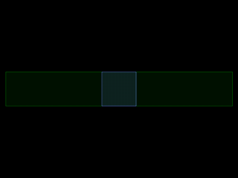
rectangle#
- gf180mcu.cells.rectangle(size=(4.0, 2.0), *, layer=<LAYER.comp: 14>, centered=False, port_type='electrical', port_orientations=(180, 90, 0, -90))#
Returns a rectangle.
- Parameters:
size (Size) – (tuple) Width and height of rectangle.
layer (LayerSpec) – Specific layer to put polygon geometry on.
centered (bool) – True sets center to (0, 0), False sets south-west to (0, 0).
port_type (str | None) – optical, electrical.
port_orientations (Ints | None) – list of port_orientations to add. None adds no ports.
- Return type:
Component
from gf180mcu import cells

c = cells.rectangle(size=(4, 2), layer='comp', centered=False, port_type='electrical', port_orientations=(180, 90, 0, -90))
c = c.copy()
c.draw_ports()
c.plot()
(Source code, png, hires.png, pdf)
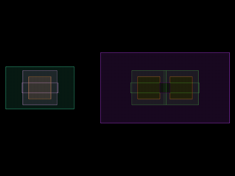
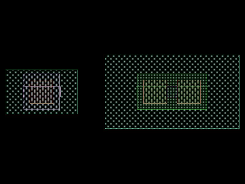
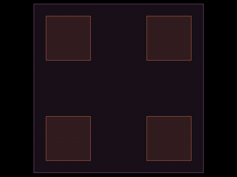
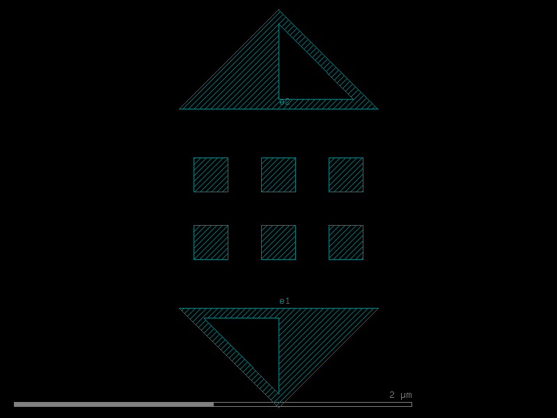
rectangle_array#
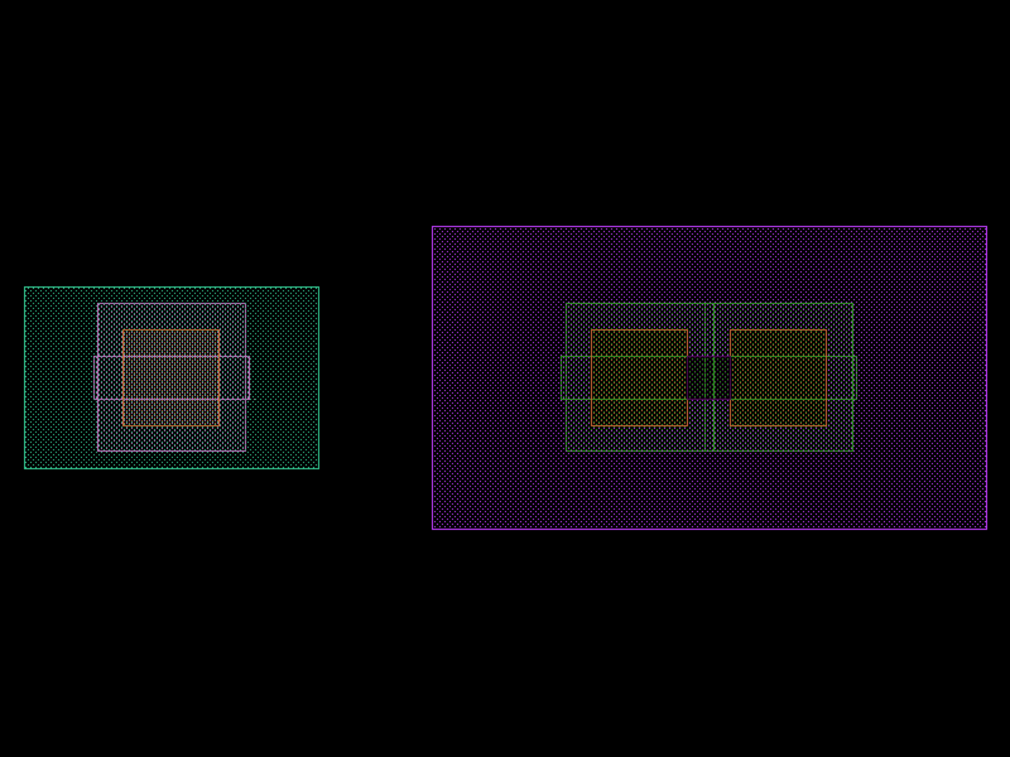
- gf180mcu.cells.rectangle_array(*, component=functools.partial(<function rectangle>, layer=<LAYER.comp: 14>), columns=6, rows=1, column_pitch=150, row_pitch=150, add_ports=True, size=None, centered=False, post_process=None, auto_rename_ports=False)#
Returns an array of components.
- Parameters:
component (ComponentSpec) – to replicate.
columns (int) – in x.
rows (int) – in y.
column_pitch (float) – pitch between columns.
row_pitch (float) – pitch between rows.
auto_rename_ports (bool) – True to auto rename ports.
add_ports (bool) – add ports from component into the array.
size (Size | None) – Optional x, y size. Overrides columns and rows.
centered (bool) – center the array around the origin.
post_process (PostProcesses | None) – function to apply to the array after creation.
- Raises:
ValueError – If columns > 1 and spacing[0] = 0.
ValueError – If rows > 1 and spacing[1] = 0.
- Return type:
Component
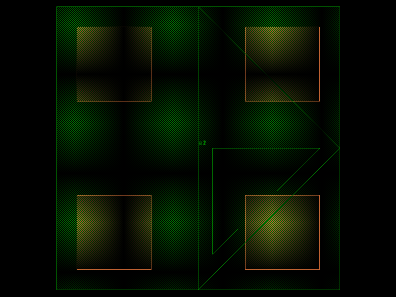
2 rows x 4 columns

  column_pitch
  <---------->
 ___        ___       ___        ___
|   |      |   |     |   |      |   |
|___|      |___|     |___|      |___|

 ___        ___       ___        ___
|   |      |   |     |   |      |   |
|___|      |___|     |___|      |___|
from gf180mcu import cells

c = cells.rectangle_array(columns=6, rows=1, column_pitch=150, row_pitch=150, add_ports=True, centered=False, auto_rename_ports=False)
c = c.copy()
c.draw_ports()
c.plot()
(Source code, png, hires.png, pdf)

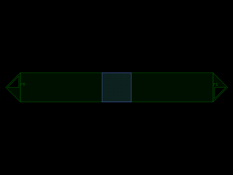
res#
- gf180mcu.cells.res(l_res=0.1, w_res=0.1, res_type='rm1', label=False, r0_label='', r1_label='')[source]#
Returns 2-terminal Metal resistor by specifying parameters.
- Parameters:
l_res (float) – length of resistor.
w_res (float) – width of resistor.
res_type (str) – type of resistor.
label (bool) – label generation.
r0_label (str) – label for resistor.
r1_label (str) – label for resistor.
- Return type:
Component
from gf180mcu import cells

c = cells.res(l_res=0.1, w_res=0.1, res_type='rm1', label=False, r0_label='', r1_label='')
c = c.copy()
c.draw_ports()
c.plot()
(Source code, png, hires.png, pdf)

sc_diode#
- gf180mcu.cells.sc_diode(la=0.1, wa=0.1, cw=0.1, m=1, pcmpgr=False, label=False, p_label='', n_label='')[source]#
Used to draw N+/LVPWELL diode (Outside DNWELL) by specifying parameters.
- Parameters:
la (float) – Float of diff length (anode)
wa (float) – Float of diff width (anode)
m (int) – Integer of number of fingers
pcmpgr (bool) – Boolean of using P+ Guard Ring for Deep NWELL devices only
cw (float)
label (bool)
p_label (str)
n_label (str)
- Return type:
Component
from gf180mcu import cells

c = cells.sc_diode(la=0.1, wa=0.1, cw=0.1, m=1, pcmpgr=False, label=False, p_label='', n_label='')
c = c.copy()
c.draw_ports()
c.plot()
(Source code, png, hires.png, pdf)

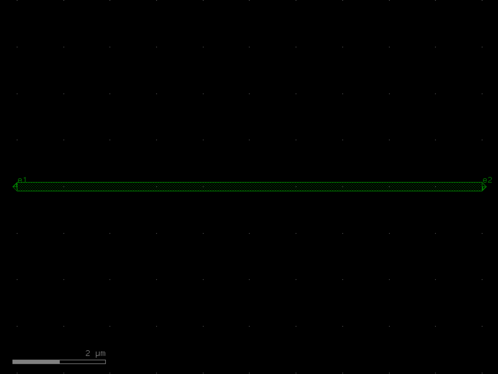
straight#
- gf180mcu.cells.straight(length=10, cross_section='metal1', width=None)[source]#
Returns a Straight waveguide.
- Parameters:
length (float) – straight length (um).
cross_section (CrossSection | str | dict[str, Any] | Callable[[...], CrossSection] | SymmetricalCrossSection | DCrossSection) – specification (CrossSection, string or dict).
width (float | None) – width of the waveguide. If None, it will use the width of the cross_section.
- Return type:
Component
from gf180mcu import cells

c = cells.straight(length=10, cross_section='metal1')
c = c.copy()
c.draw_ports()
c.plot()
(Source code, png, hires.png, pdf)

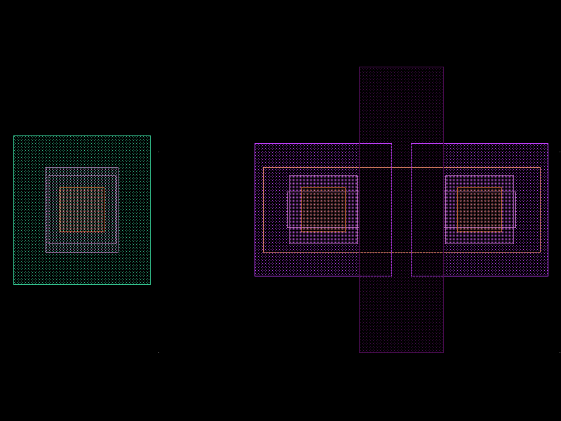
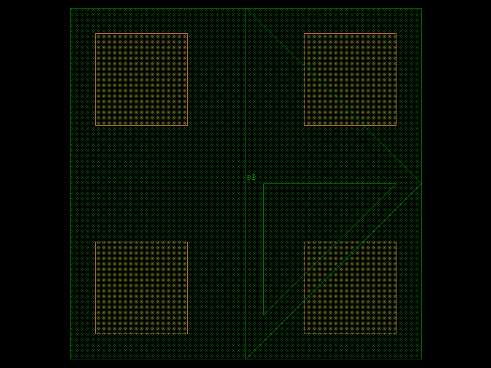
via_generator#
- gf180mcu.cells.via_generator(x_range=(0, 1), y_range=(0, 1), via_size=(0.17, 0.17), via_layer=(66, 44), via_enclosure=(0.06, 0.06), via_spacing=(0.17, 0.17))[source]#
Return only vias withen the range xrange and yrange while enclosing by via_enclosure and set number of rows and number of columns according to ranges and via size and spacing.
- Parameters:
x_range (tuple[float, float]) – dx range.
y_range (tuple[float, float]) – dy range.
via_size (tuple[float, float]) – via size.
via_layer (tuple[int, int] | str | int | LayerEnum) – via layer.
via_enclosure (tuple[float, float]) – via enclosure.
via_spacing (tuple[float, float]) – via spacing.
- Return type:
Component
from gf180mcu import cells

c = cells.via_generator(x_range=(0, 1), y_range=(0, 1), via_size=(0.17, 0.17), via_layer=(66, 44), via_enclosure=(0.06, 0.06), via_spacing=(0.17, 0.17))
c = c.copy()
c.draw_ports()
c.plot()
(Source code, png, hires.png, pdf)
via_stack#
- gf180mcu.cells.via_stack(x_range=(0, 1), y_range=(0, 1), metal_level=1, con_size=(0.22, 0.22), con_enc=0.07, m_enc=0.06, con_spacing=(0.28, 0.28), via_size=(0.22, 0.22), via_spacing=(0.28, 0.28), via_enc=(0.06, 0.06), base_layer=<LAYER.metal1: 10>, **kwargs)[source]#
Returns a via stack withen the range xrange and yrange and expecting the base_layer to be drawen.
- Parameters:
x_range (tuple[float, float]) – dx range.
y_range (tuple[float, float]) – dy range.
metal_level (int) – metal level.
con_size (tuple[float, float]) – contact size.
con_enc (float) – contact enclosure.
m_enc (float) – metal enclosure.
con_spacing (tuple[float, float]) – contact spacing.
via_size (tuple[float, float]) – via size.
via_spacing (tuple[float, float]) – via spacing.
via_enc (tuple[float, float]) – via enclosure.
base_layer (tuple[int, int] | str | int | LayerEnum)
kwargs (Any)
- Return type:
Component
return via stack till the metal level indicated where : metal_level 1 : till m1 metal_level 2 : till m2 metal_level 3 : till m3 metal_level 4 : till m4 metal_level 5 : till m5 withen the range xrange and yrange and expecting the base_layer to be drawen
from gf180mcu import cells

c = cells.via_stack(x_range=(0, 1), y_range=(0, 1), metal_level=1, con_size=(0.22, 0.22), con_enc=0.07, m_enc=0.06, con_spacing=(0.28, 0.28), via_size=(0.22, 0.22), via_spacing=(0.28, 0.28), via_enc=(0.06, 0.06), base_layer='metal1')
c = c.copy()
c.draw_ports()
c.plot()
(Source code, png, hires.png, pdf)
well_res#
- gf180mcu.cells.well_res(l_res=0.42, w_res=0.42, res_type='nwell', pcmpgr=False, label=False, r0_label='', r1_label='', sub_label='')[source]#
- Parameters:
l_res (float)
w_res (float)
res_type (str)
pcmpgr (bool)
label (bool)
r0_label (str)
r1_label (str)
sub_label (str)
- Return type:
Component
from gf180mcu import cells

c = cells.well_res(l_res=0.42, w_res=0.42, res_type='nwell', pcmpgr=False, label=False, r0_label='', r1_label='', sub_label='')
c = c.copy()
c.draw_ports()
c.plot()
(Source code, png, hires.png, pdf)

wire_corner#
- gf180mcu.cells.wire_corner(cross_section='metal2', width=None)[source]#
Returns 45 degrees electrical corner wire.
- Parameters:
cross_section (CrossSection | str | dict[str, Any] | Callable[[...], CrossSection] | SymmetricalCrossSection | DCrossSection) – spec.
width (float | None) – optional width. Defaults to cross_section width.
- Return type:
Component
from gf180mcu import cells

c = cells.wire_corner(cross_section='metal2')
c = c.copy()
c.draw_ports()
c.plot()
(Source code, png, hires.png, pdf)

wire_corner45#
- gf180mcu.cells.wire_corner45(cross_section='metal2', radius=10, width=None, layer=None, with_corner90_ports=True)[source]#
Returns 90 degrees electrical corner wire.
- Parameters:
cross_section (CrossSection | str | dict[str, Any] | Callable[[...], CrossSection] | SymmetricalCrossSection | DCrossSection) – spec.
radius (float) – ignored.
width (float | None) – optional width. Defaults to cross_section width.
layer (tuple[int, int] | str | int | LayerEnum | None) – ignored.
with_corner90_ports (bool) – if True, adds ports at 90 degrees.
- Return type:
Component
from gf180mcu import cells

c = cells.wire_corner45(cross_section='metal2', radius=10, with_corner90_ports=True)
c = c.copy()
c.draw_ports()
c.plot()
(Source code, png, hires.png, pdf)