KCell Enclosure
KCellEnclosure is the cell-level counterpart to LayerEnclosure. Where
LayerEnclosure processes the geometry of a single component, KCellEnclosure:
- Recurses into all sub-cells (
begin_shapes_rec) to collect geometry. - Merges the collected geometry into one
Regionbefore computing the expansion. - Applies one or more
LayerEnclosurerules in a single pass.
This guarantees a continuous cladding across component joints — no gaps at the seams between adjacent waveguides or bends.
| Class | Scope | Gap-free joins |
|---|---|---|
LayerEnclosure |
one component at a time | no — each component enclosed separately |
KCellEnclosure |
entire assembled cell | yes — geometry merged first |
The Layer Enclosure page introduces LayerEnclosure and shows a
basic KCellEnclosure example. This page covers advanced usage: multiple enclosures,
tiling parameters, and the directional Minkowski methods.
Setup
import kfactory as kf


class LAYER(kf.LayerInfos):
    WG: kf.kdb.LayerInfo = kf.kdb.LayerInfo(1, 0)
    WGCLAD: kf.kdb.LayerInfo = kf.kdb.LayerInfo(2, 0)
    SLAB: kf.kdb.LayerInfo = kf.kdb.LayerInfo(3, 0)
    NPP: kf.kdb.LayerInfo = kf.kdb.LayerInfo(4, 0)
    DEEPOX: kf.kdb.LayerInfo = kf.kdb.LayerInfo(5, 0)


L = LAYER()
kf.kcl.infos = L
1 · Single enclosure
The minimal usage: wrap one LayerEnclosure in a KCellEnclosure and call
apply_minkowski_tiled on the finished cell.
The key rules are:
- Call apply_minkowski_tiled inside the @kf.cell function, before return c.
- The LayerEnclosure must have main_layer set so the processor knows which layer
to expand.
clad_enc = kf.LayerEnclosure(
dsections=[(L.WGCLAD, 2.0)],
name="WG_CLAD",
main_layer=L.WG,
kcl=kf.kcl,
)
kcell_enc = kf.KCellEnclosure([clad_enc])
@kf.cell
def bend_pair_clad(radius: float, width: float) -> kf.KCell:
"""Two euler bends placed close together with unified cell-level cladding."""
c = kf.KCell()
bend_fn = kf.factories.euler.bend_euler_factory(kcl=kf.kcl)
b1 = c << bend_fn(width=width, radius=radius, layer=L.WG, angle=90)
b2 = c << bend_fn(width=width, radius=radius, layer=L.WG, angle=90)
# Mirror b2 so it curves the opposite direction, then offset it by
# 1.5 µm in y. The two WG cores stay well-separated (1.5 µm apart at
# the closest point) but the 2 µm cladding rings overlap by ~2.5 µm —
# exactly the case `KCellEnclosure` is meant to handle: merging
# interacting claddings into a single continuous region without one
# cancelling the other.
b2.dmirror_y()
b2.dmove((0, 0), (0, -1.5))
c.add_ports(b1.ports.filter(port_type="optical"))
c.add_ports(b2.ports.filter(port_type="optical"))
c.auto_rename_ports()
# Apply unified cladding to the finished assembly
kcell_enc.apply_minkowski_tiled(c)
return c
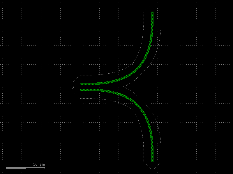
bend_pair_clad(radius=10, width=0.5).plot()
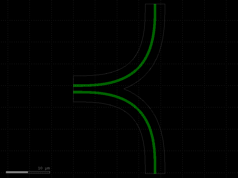
Both bends' cladding rings would normally be drawn separately by
LayerEnclosure (one per component) and would overlap visibly as two
distinct annular bands. KCellEnclosure merges the cell geometry first,
so the two interacting claddings come out as a single continuous region
with no spurious gaps where they meet.
2 · Multiple enclosures in one KCellEnclosure
Pass a list of LayerEnclosure objects to cover several output layers in a single
apply_minkowski_tiled call. The processor iterates over them in order.
slab_enc = kf.LayerEnclosure(
    dsections=[(L.SLAB, 3.0)],
    name="WG_SLAB",
    main_layer=L.WG,
    kcl=kf.kcl,
)

npp_enc = kf.LayerEnclosure(
    dsections=[(L.NPP, 1.0, 4.0)],  # annular: 1 µm to 4 µm from WG edge
    name="WG_NPP",
    main_layer=L.WG,
    kcl=kf.kcl,
)

# Combine three enclosures: cladding + slab + implant
multi_enc = kf.KCellEnclosure([clad_enc, slab_enc, npp_enc])


@kf.cell
def bend_pair_multi(radius: float, width: float) -> kf.KCell:
    """Two euler bends with multi-layer cell-level enclosure."""
    c = kf.KCell()
    bend_fn = kf.factories.euler.bend_euler_factory(kcl=kf.kcl)

    b1 = c << bend_fn(width=width, radius=radius, layer=L.WG, angle=90)
    b2 = c << bend_fn(width=width, radius=radius, layer=L.WG, angle=90)
    # Same close-but-unconnected placement as in section 1.
    b2.dmirror_y()
    b2.dmove((0, 0), (0, -1.5))

    c.add_ports(b1.ports.filter(port_type="optical"))
    c.add_ports(b2.ports.filter(port_type="optical"))
    c.auto_rename_ports()

    multi_enc.apply_minkowski_tiled(c)
    return c


bend_pair_multi(radius=10, width=0.5).plot()
[32m2026-06-05 00:50:52.288[0m | [31m[1mERROR [0m | [36mkfactory.kcell[0m:[36mname[0m:[36m702[0m - [31m[1mName conflict in kfactory.kcell::name at line 702
Renaming Unnamed_4 (cell_index=4) to bend_euler_W0p5_R10_LWG_ENone_A90_R150 would cause it to be named the same as:
- bend_euler_W0p5_R10_LWG_ENone_A90_R150 (cell_index=1), function_name=bend_euler, basename=None[0m
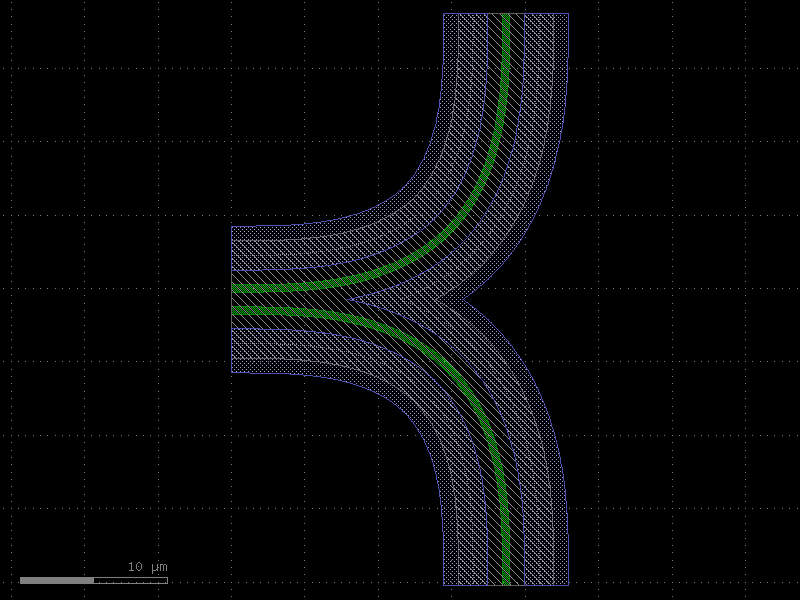
Three generated layers are visible: - WGCLAD — 2 µm uniform cladding - SLAB — 3 µm uniform slab - NPP — annular implant from 1 µm to 4 µm outside the WG edge
3 · Tiling parameters
apply_minkowski_tiled uses KLayout's TilingProcessor for parallel computation.
The key parameters are:
| Parameter | Default | Effect |
|---|---|---|
tile_size |
None (auto) |
Tile edge length in µm. Auto = max(10×max_d, 200 µm). |
n_pts |
64 | Points in the circular kernel. Fewer = faster but more angular corners. |
n_threads |
None (all CPUs) |
Override thread count (useful in CI). |
carve_out_ports |
True |
Remove cladding from port openings so waveguides remain accessible. |
Effect of n_pts on corner shape
enc_coarse = kf.KCellEnclosure([clad_enc])
enc_fine = kf.KCellEnclosure([clad_enc])
@kf.cell
def single_bend_npts(radius: float, width: float, n_pts: int) -> kf.KCell:
"""Euler bend with variable n_pts for corner resolution."""
c = kf.KCell()
b = c << kf.factories.euler.bend_euler_factory(kcl=kf.kcl)(
width=width, radius=radius, layer=L.WG, angle=90
)
c.add_ports(b.ports)
c.auto_rename_ports()
kf.KCellEnclosure([clad_enc]).apply_minkowski_tiled(c, n_pts=n_pts)
return c
# n_pts=8 → octagonal corners
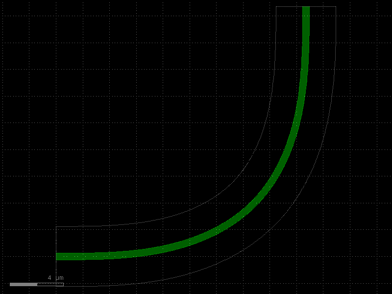
single_bend_npts(radius=10, width=0.5, n_pts=8).plot()
[32m2026-06-05 00:50:52.791[0m | [31m[1mERROR [0m | [36mkfactory.kcell[0m:[36mname[0m:[36m702[0m - [31m[1mName conflict in kfactory.kcell::name at line 702
Renaming Unnamed_7 (cell_index=7) to bend_euler_W0p5_R10_LWG_ENone_A90_R150 would cause it to be named the same as:
- bend_euler_W0p5_R10_LWG_ENone_A90_R150 (cell_index=1), function_name=bend_euler, basename=None
- bend_euler_W0p5_R10_LWG_ENone_A90_R150 (cell_index=4), function_name=bend_euler, basename=None[0m

With n_pts=8 the corners of the WGCLAD are octagonal. The default n_pts=64
produces near-circular corners.
# n_pts=64 → smooth circular corners (default)
single_bend_npts(radius=10, width=0.5, n_pts=64).plot()
[32m2026-06-05 00:50:52.865[0m | [31m[1mERROR [0m | [36mkfactory.kcell[0m:[36mname[0m:[36m702[0m - [31m[1mName conflict in kfactory.kcell::name at line 702
Renaming Unnamed_10 (cell_index=10) to bend_euler_W0p5_R10_LWG_ENone_A90_R150 would cause it to be named the same as:
- bend_euler_W0p5_R10_LWG_ENone_A90_R150 (cell_index=1), function_name=bend_euler, basename=None
- bend_euler_W0p5_R10_LWG_ENone_A90_R150 (cell_index=4), function_name=bend_euler, basename=None
- bend_euler_W0p5_R10_LWG_ENone_A90_R150 (cell_index=7), function_name=bend_euler, basename=None[0m
Controlling threads for CI environments
# Use a fixed thread count for reproducible timing in CI
kcell_enc.apply_minkowski_tiled(c, n_threads=1)
4 · apply_minkowski_y — directional enclosure for horizontal waveguides
apply_minkowski_tiled uses a circle as the Minkowski kernel, producing rounded
corners on all sides. For horizontal straight waveguides this is often
undesirable — you want the cladding to extend only above and below the waveguide
(Y direction) without rounding the ends.
apply_minkowski_y uses a vertical edge (0, −d) → (0, d) as the kernel:
- Expands in the Y direction by d.
- No expansion in the X direction — cladding ends flush with the waveguide ends.
This is useful when the port openings must remain clear, or when the cladding rectangle must match the exact waveguide length.
clad_enc_y = kf.LayerEnclosure(
    dsections=[(L.WGCLAD, 1.5)],
    name="CLAD_Y",
    main_layer=L.WG,
    kcl=kf.kcl,
)
kcell_enc_y = kf.KCellEnclosure([clad_enc_y])


@kf.cell
def straight_clad_y(length: float, width: float) -> kf.KCell:
    """Horizontal straight waveguide with Y-only cladding."""
    c = kf.KCell()
    s = c << kf.factories.straight.straight_dbu_factory(kcl=kf.kcl)(
        length=kf.kcl.to_dbu(length),
        width=kf.kcl.to_dbu(width),
        layer=L.WG,
    )
    c.add_ports(s.ports)
    c.auto_rename_ports()
    # Expand cladding in Y only — no rounding at port ends
    kcell_enc_y.apply_minkowski_y(c)
    return c


straight_clad_y(length=20.0, width=0.5).plot()
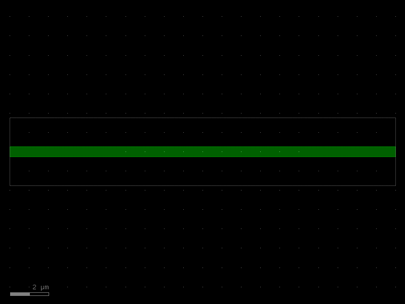
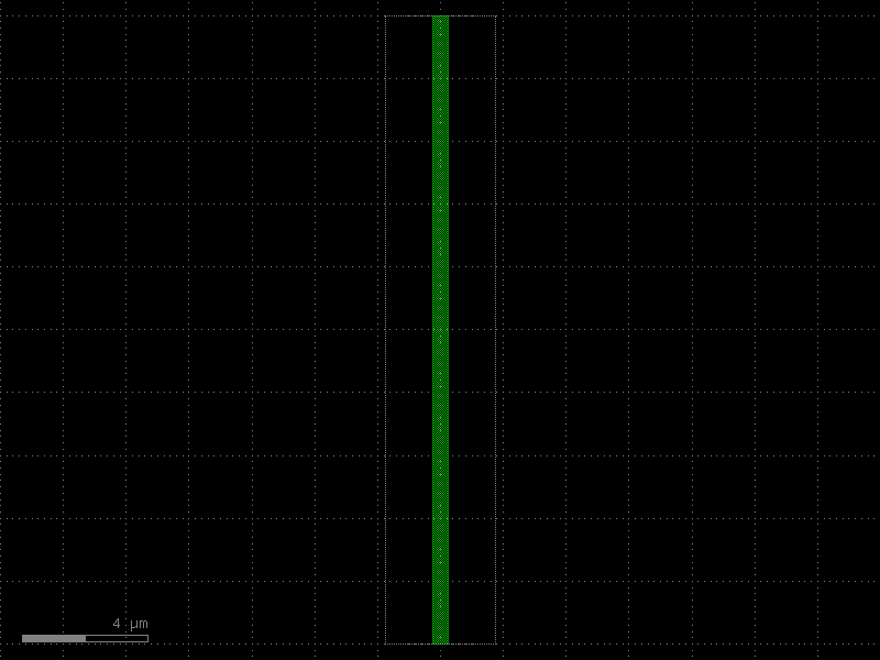
The WGCLAD (layer 2/0) extends 1.5 µm above and below the waveguide but ends exactly at the port faces — no overextension at the ends.
5 · apply_minkowski_x — directional enclosure for vertical waveguides
apply_minkowski_x is the X-direction counterpart. It uses a horizontal edge
(−d, 0) → (d, 0) as the kernel, expanding only left and right. This is the
correct choice for waveguides oriented vertically (angle 90° / 270°).
kcell_enc_x = kf.KCellEnclosure([clad_enc_y])


@kf.cell
def vertical_straight_clad_x(length: float, width: float) -> kf.KCell:
    """Vertical straight waveguide with X-only cladding."""
    c = kf.KCell()
    s = c << kf.factories.straight.straight_dbu_factory(kcl=kf.kcl)(
        length=kf.kcl.to_dbu(length),
        width=kf.kcl.to_dbu(width),
        layer=L.WG,
    )
    # Rotate 90° so the waveguide runs vertically
    s.drotate(90)
    c.add_ports(s.ports)
    c.auto_rename_ports()
    kcell_enc_x.apply_minkowski_x(c)
    return c


vertical_straight_clad_x(length=20.0, width=0.5).plot()
[32m2026-06-05 00:50:53.053[0m | [31m[1mERROR [0m | [36mkfactory.kcell[0m:[36mname[0m:[36m702[0m - [31m[1mName conflict in kfactory.kcell::name at line 702
Renaming Unnamed_16 (cell_index=16) to straight_W500_L20000_LWG_ENone would cause it to be named the same as:
- straight_W500_L20000_LWG_ENone (cell_index=13), function_name=straight, basename=None[0m
6 · apply_minkowski_custom — custom kernel shape
For full control over the expansion shape pass a callable to
apply_minkowski_custom. The callable receives the expansion distance d (in DBU)
and must return a kdb.Edge, kdb.Polygon, or kdb.Box.
Diamond kernel
A diamond (rotated square) rounds corners at 45° — a good compromise between a box (very angular) and a circle (many points, slower).
def diamond(d: int) -> kf.kdb.Polygon:
    """Return a diamond-shaped polygon with half-diagonal d."""
    return kf.kdb.Polygon(
        [
            kf.kdb.Point(0, d),
            kf.kdb.Point(d, 0),
            kf.kdb.Point(0, -d),
            kf.kdb.Point(-d, 0),
        ]
    )


kcell_enc_diamond = kf.KCellEnclosure([clad_enc])


@kf.cell
def bend_pair_diamond(radius: float, width: float) -> kf.KCell:
    """Two euler bends with diamond-kernel cell-level cladding."""
    c = kf.KCell()
    bend_fn = kf.factories.euler.bend_euler_factory(kcl=kf.kcl)

    b1 = c << bend_fn(width=width, radius=radius, layer=L.WG, angle=90)
    b2 = c << bend_fn(width=width, radius=radius, layer=L.WG, angle=90)
    # Same close-but-unconnected placement as in section 1.
    b2.dmirror_y()
    b2.dmove((0, 0), (0, -1.5))

    c.add_ports(b1.ports.filter(port_type="optical"))
    c.add_ports(b2.ports.filter(port_type="optical"))
    c.auto_rename_ports()

    kcell_enc_diamond.apply_minkowski_custom(c, shape=diamond)
    return c


bend_pair_diamond(radius=10, width=0.5).plot()
[32m2026-06-05 00:50:53.140[0m | [31m[1mERROR [0m | [36mkfactory.kcell[0m:[36mname[0m:[36m702[0m - [31m[1mName conflict in kfactory.kcell::name at line 702
Renaming Unnamed_19 (cell_index=19) to bend_euler_W0p5_R10_LWG_ENone_A90_R150 would cause it to be named the same as:
- bend_euler_W0p5_R10_LWG_ENone_A90_R150 (cell_index=1), function_name=bend_euler, basename=None
- bend_euler_W0p5_R10_LWG_ENone_A90_R150 (cell_index=4), function_name=bend_euler, basename=None
- bend_euler_W0p5_R10_LWG_ENone_A90_R150 (cell_index=7), function_name=bend_euler, basename=None
- bend_euler_W0p5_R10_LWG_ENone_A90_R150 (cell_index=10), function_name=bend_euler, basename=None[0m
The WGCLAD corners are diamond-shaped (45° chamfers).
7 · Method reference
| Method | Kernel | Expands | Best for |
|---|---|---|---|
apply_minkowski_tiled |
circle (n_pts points) |
all directions | complex / curved cells |
apply_minkowski_y |
vertical edge | Y only | horizontal straight waveguides |
apply_minkowski_x |
horizontal edge | X only | vertical straight waveguides |
apply_minkowski_custom(c, shape) |
user-supplied | custom | custom corner shapes |
Directional method comparison
| Method | Corners | Port openings | Computation |
|---|---|---|---|
apply_minkowski_tiled |
rounded | carved out (carve_out_ports=True) |
tiled, parallel |
apply_minkowski_y |
square (no rounding) | flush at port ends | single-pass |
apply_minkowski_x |
square (no rounding) | flush at port ends | single-pass |
apply_minkowski_custom |
matches kernel | depends on kernel | single-pass |
Quick-start checklist
- Always set
main_layer=on everyLayerEnclosureused insideKCellEnclosure. - Call the apply method inside the
@kf.cellfunction, beforereturn c. - For large or curved cells use
apply_minkowski_tiled(parallel, circle kernel). - For straight waveguides use
apply_minkowski_y/apply_minkowski_xto keep cladding flush with port faces. - Adjust
n_ptsinapply_minkowski_tiledto trade corner resolution for speed.
See Also
| Topic | Where |
|---|---|
| Layer enclosures (single-layer) | Enclosures: Layer Enclosure |
| Cross-sections (port geometry) | Cross-Sections |
| Boolean / region operations | Core Concepts: Geometry |
| Tile-based fill | Utilities: Fill |