Parametric Cells#
Here are the parametric components available in the PDK.
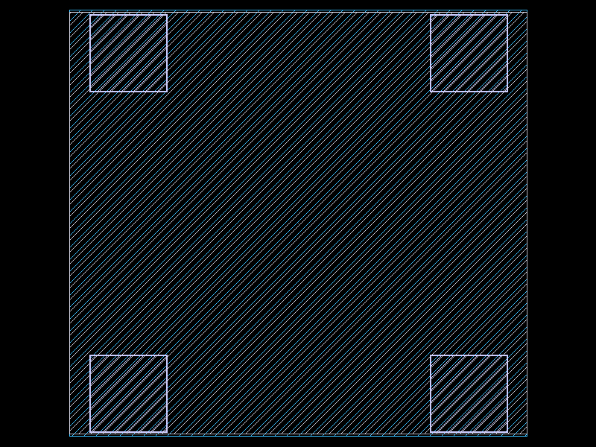
add_pads_top#
- ihp.cells.add_pads_top(component='straight', port_names=None, component_name=None, cross_section='metal_routing', pad_port_name='e1', pad='CuPillarPad_fixed', bend='wire_corner', straight_separation=15.0, pad_pitch=100.0, taper=None, port_type='electrical', allow_width_mismatch=True, fanout_length=80, route_width=0, **kwargs)[source]#
Returns new component with ports connected top pads.
- Parameters:
component (str | Callable[[...], Component] | dict[str, Any] | DKCell | partial[Component]) – component spec to connect to.
port_names (Sequence[str] | None) – list of port names to connect to pads.
component_name (str | None) – optional for the label.
cross_section (CrossSection | str | dict[str, Any] | Callable[[...], CrossSection] | SymmetricalCrossSection | DCrossSection) – cross_section function.
pad_port_name (str) – pad port name.
pad (str | Callable[[...], Component] | dict[str, Any] | DKCell | partial[Component]) – pad function.
bend (str | Callable[[...], Component] | dict[str, Any] | DKCell | partial[Component]) – bend function.
straight_separation (float) – from edge to edge.
pad_pitch (float) – spacing between pads.
taper (str | Callable[[...], Component] | dict[str, Any] | DKCell | partial[Component] | None) – taper function.
port_type (str) – port type.
allow_width_mismatch (bool) – if True, allows width mismatch.
fanout_length (float | None) – length of the fanout.
route_width (float | list[float] | None) – width of the route.
kwargs – additional arguments.
- Return type:
Component
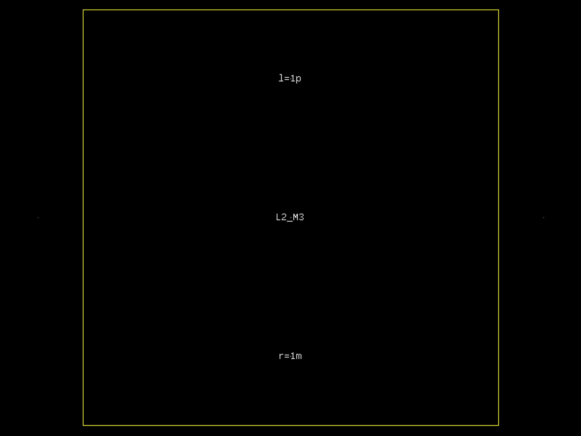
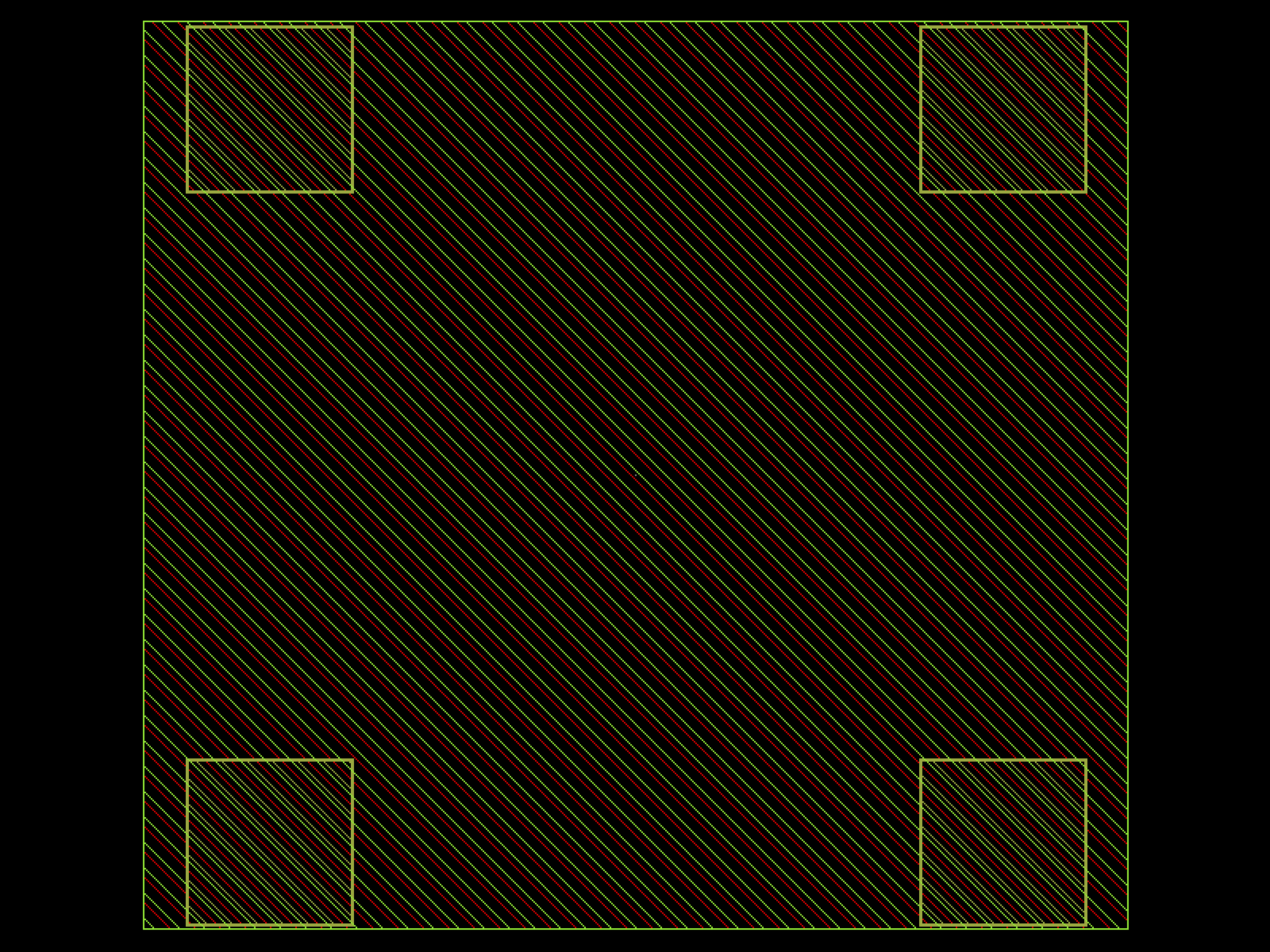
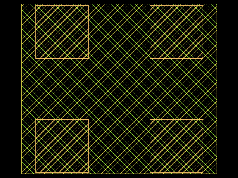
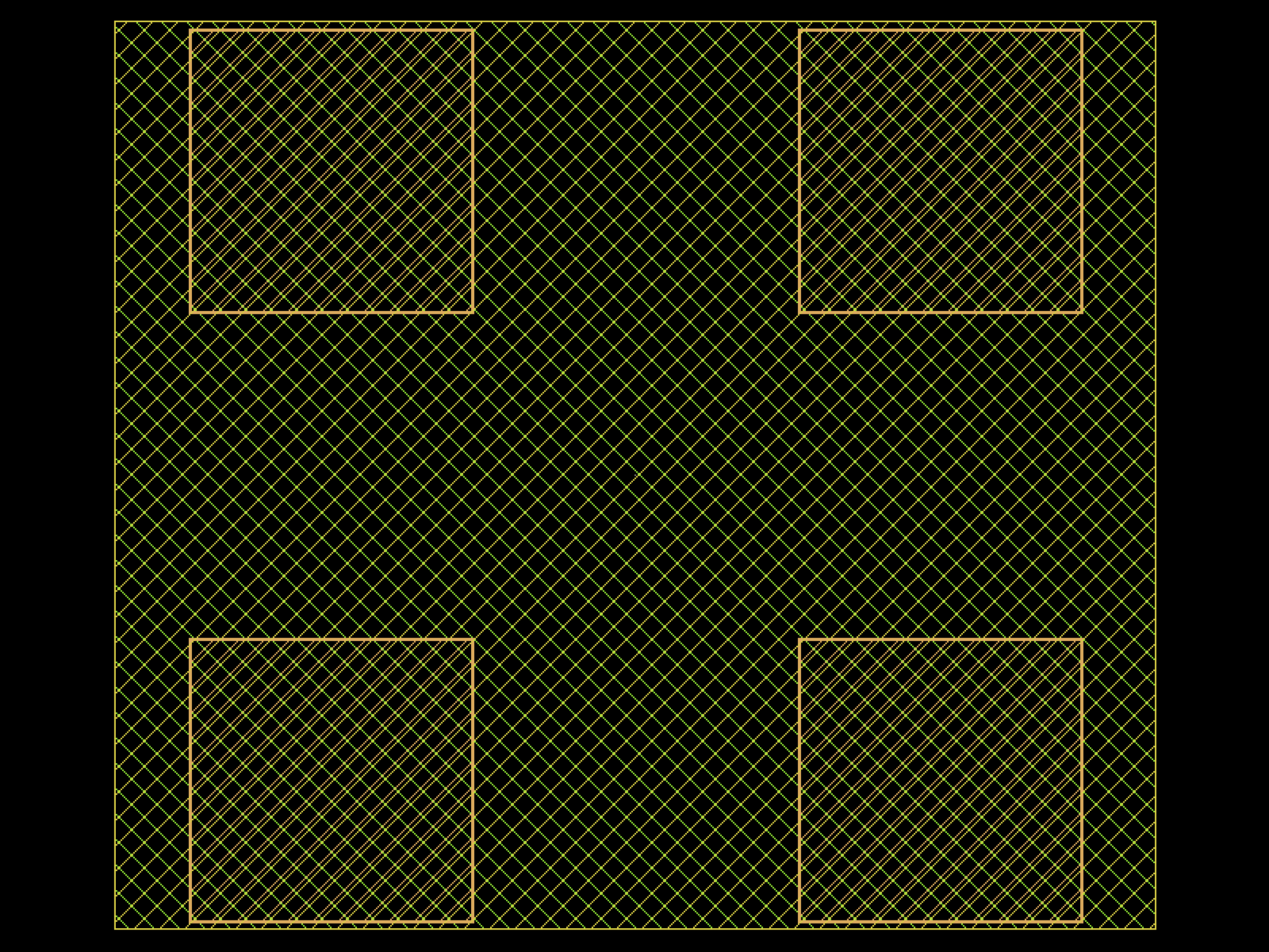
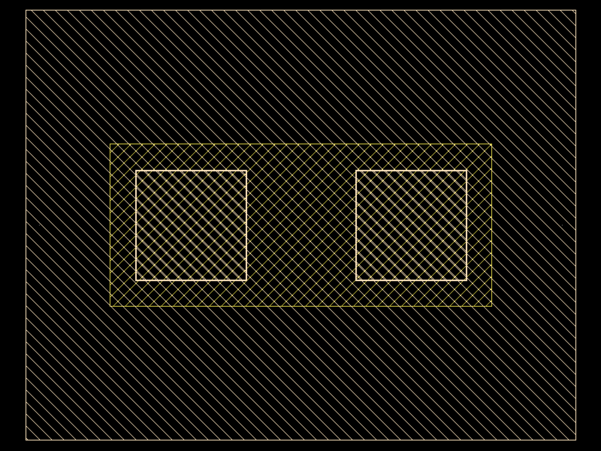
import gdsfactory as gf
c = gf.c.nxn(
    xsize=600,
    ysize=200,
    north=2,
    south=3,
    wg_width=10,
    layer="M3",
    port_type="electrical",
)
cc = gf.routing.add_pads_top(component=c, port_names=("e1", "e4"), fanout_length=50)
cc.plot()
import warnings
warnings.filterwarnings("ignore", category=DeprecationWarning)

from ihp import PDK
from ihp import cells

PDK.activate()

c = cells.add_pads_top(component='straight', cross_section='metal_routing', pad_port_name='e1', pad='CuPillarPad_fixed', bend='wire_corner', straight_separation=15.0, pad_pitch=100.0, port_type='electrical', allow_width_mismatch=True, fanout_length=80, route_width=0).copy()
c.draw_ports()
c.plot()
(Source code, png, hires.png, pdf)

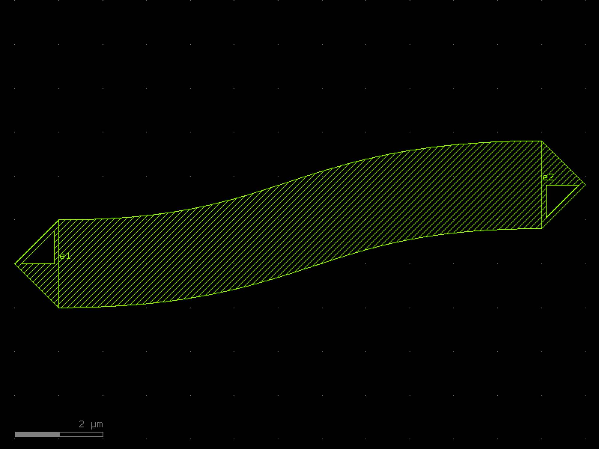
bend_euler#
- ihp.cells.bend_euler(radius=None, angle=90, p=0.5, width=None, cross_section='strip', allow_min_radius_violation=False)[source]#
Regular degree euler bend.
- Parameters:
radius (float | None) – in um. Defaults to cross_section_radius.
angle (float) – total angle of the curve.
p (float) – Proportion of the curve that is an Euler curve.
width (float | None) – width to use. Defaults to cross_section.width.
cross_section (CrossSection | str | dict[str, Any] | Callable[[...], CrossSection] | SymmetricalCrossSection | DCrossSection) – specification (CrossSection, string, CrossSectionFactory dict).
allow_min_radius_violation (bool) – if True allows radius to be smaller than cross_section radius.
- Return type:
Component
import warnings
warnings.filterwarnings("ignore", category=DeprecationWarning)

from ihp import PDK
from ihp import cells

PDK.activate()

c = cells.bend_euler(angle=90, p=0.5, cross_section='strip', allow_min_radius_violation=False).copy()
c.draw_ports()
c.plot()
(Source code, png, hires.png, pdf)

bend_metal#
- ihp.cells.bend_metal(radius=None, angle=90, width=None, cross_section='metal_routing')[source]#
Regular degree euler bend.
- Parameters:
radius (float | None) – None.
angle (float) –
width (float | None) – None.
cross_section (CrossSection | str | dict[str, Any] | Callable[[...], CrossSection] | SymmetricalCrossSection | DCrossSection) – “metal_routing”.
- Return type:
Component
import warnings
warnings.filterwarnings("ignore", category=DeprecationWarning)

from ihp import PDK
from ihp import cells

PDK.activate()

c = cells.bend_metal(angle=90, cross_section='metal_routing').copy()
c.draw_ports()
c.plot()
(Source code, png, hires.png, pdf)

bend_s#
- ihp.cells.bend_s(size=(11, 1.8), cross_section='strip', width=None, allow_min_radius_violation=False)[source]#
Return S bend with bezier curve.
stores min_bend_radius property in self.info[‘min_bend_radius’] min_bend_radius depends on height and length
- Parameters:
size (tuple[float, float]) – in x and y direction.
cross_section (CrossSection | str | dict[str, Any] | Callable[[...], CrossSection] | SymmetricalCrossSection | DCrossSection) – spec.
width (float | None) – width of the waveguide. If None, it will use the width of the cross_section.
allow_min_radius_violation (bool) – allows min radius violations.
- Return type:
Component
import warnings
warnings.filterwarnings("ignore", category=DeprecationWarning)

from ihp import PDK
from ihp import cells

PDK.activate()

c = cells.bend_s(size=(11, 1.8), cross_section='strip', allow_min_radius_violation=False).copy()
c.draw_ports()
c.plot()
(Source code, png, hires.png, pdf)

bend_s_metal#
- ihp.cells.bend_s_metal(size=(11, 1.8), cross_section='metal_routing', width=None, allow_min_radius_violation=True)[source]#
Return S bend with bezier curve.
stores min_bend_radius property in self.info[‘min_bend_radius’] min_bend_radius depends on height and length
- Parameters:
size (tuple[float, float]) – in x and y direction.
cross_section (CrossSection | str | dict[str, Any] | Callable[[...], CrossSection] | SymmetricalCrossSection | DCrossSection) – spec.
width (float | None) – width of the waveguide. If None, it will use the width of the cross_section.
allow_min_radius_violation (bool) – allows min radius violations.
- Return type:
Component
import warnings
warnings.filterwarnings("ignore", category=DeprecationWarning)

from ihp import PDK
from ihp import cells

PDK.activate()

c = cells.bend_s_metal(size=(11, 1.8), cross_section='metal_routing', allow_min_radius_violation=True).copy()
c.draw_ports()
c.plot()
(Source code, png, hires.png, pdf)

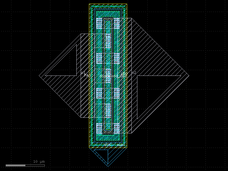
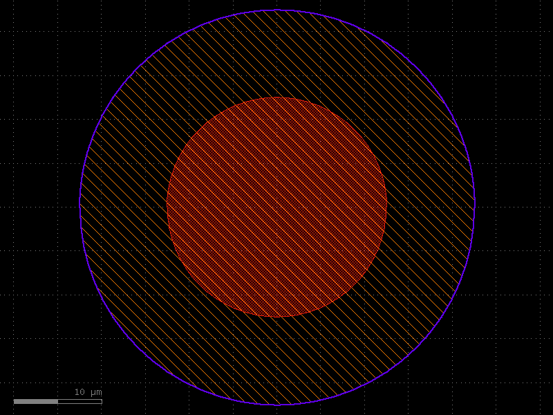
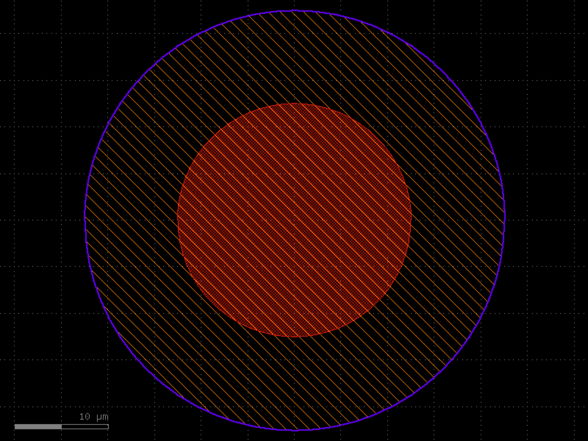
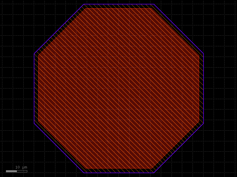
bondpad#
- ihp.cells.bondpad(shape='octagon', diameter=80.0, layer_top_metal='TopMetal2drawing', layer_top_metal_pin='TopMetal2pin', layer_passiv='Passivpillar', layer_dfpad='dfpaddrawing', bbox_offsets=(-2.1, 0), flip_chip=False)[source]#
Create a bondpad for wire bonding or flip-chip connection.
- Parameters:
shape (Literal['octagon', 'square', 'circle']) – Shape of the top-metal bondpad (“octagon”, “square”, or “circle”).
diameter (float) – Interpreted as across-flats for octagons / squares, and diameter for circles.
layer_top_metal (tuple[int, int] | str | int | LayerEnum) – Top metal layer.
layer_passiv (tuple[int, int] | str | int | LayerEnum) – Passivation-opening layer.
layer_dfpad (tuple[int, int] | str | int | LayerEnum) – Deep-fill or density-fill support layer.
bbox_offsets (tuple[float, ...] | None) – Per-layer expansion distances in micrometers, applied to the passivation and dfpad layers.
flip_chip (bool) – If True, suppress passivation opening for flip-chip bumps.
layer_top_metal_pin (tuple[int, int] | str | int | LayerEnum)
- Returns:
Component containing the complete bondpad stack.
- Return type:
Component
import warnings
warnings.filterwarnings("ignore", category=DeprecationWarning)

from ihp import PDK
from ihp import cells

PDK.activate()

c = cells.bondpad(shape='octagon', diameter=80.0, layer_top_metal='TopMetal2drawing', layer_top_metal_pin='TopMetal2pin', layer_passiv='Passivpillar', layer_dfpad='dfpaddrawing', bbox_offsets=(-2.1, 0), flip_chip=False).copy()
c.draw_ports()
c.plot()
(Source code, png, hires.png, pdf)
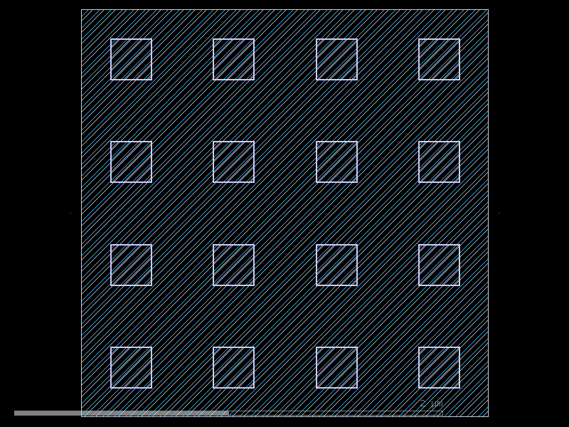
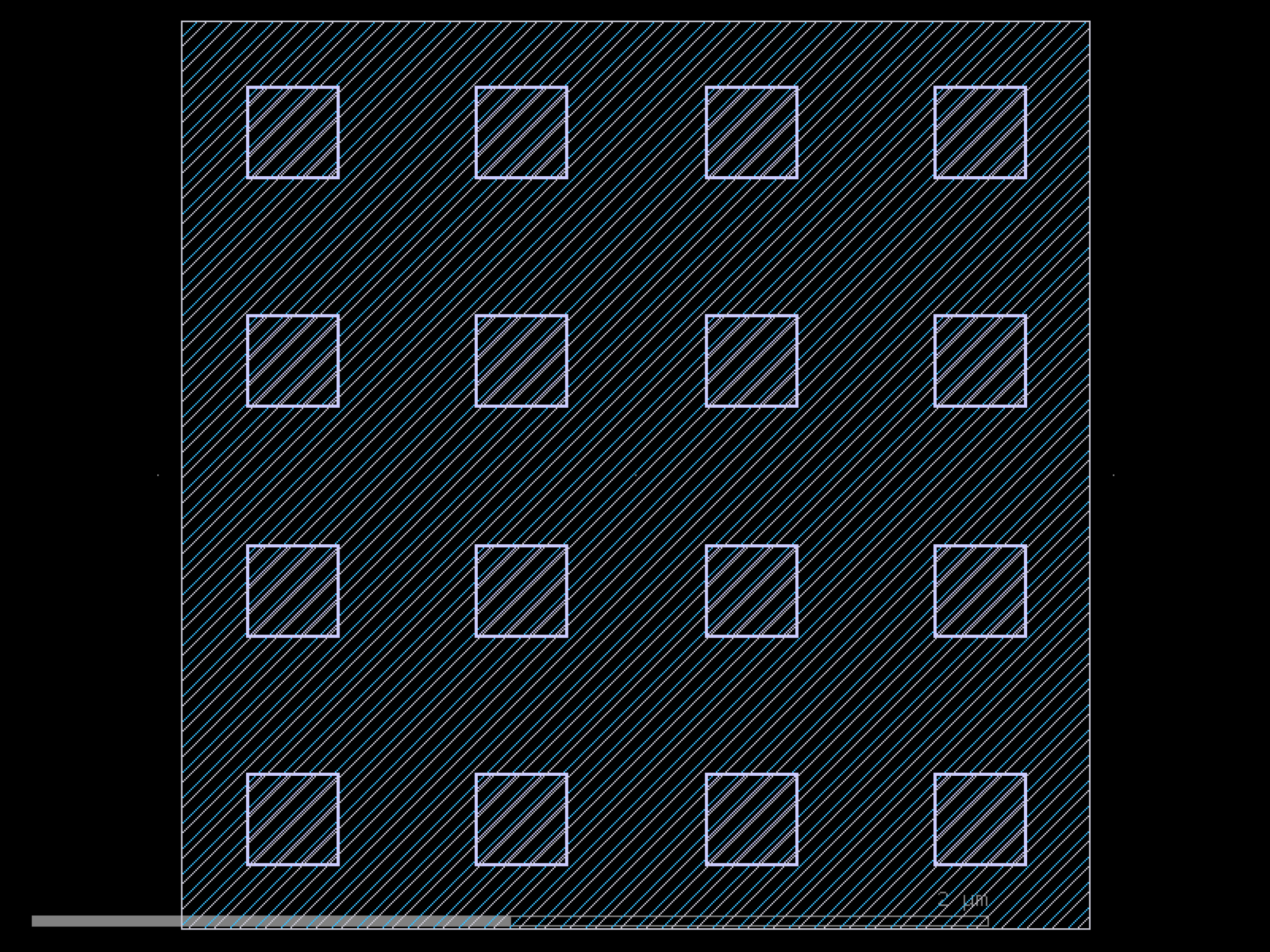
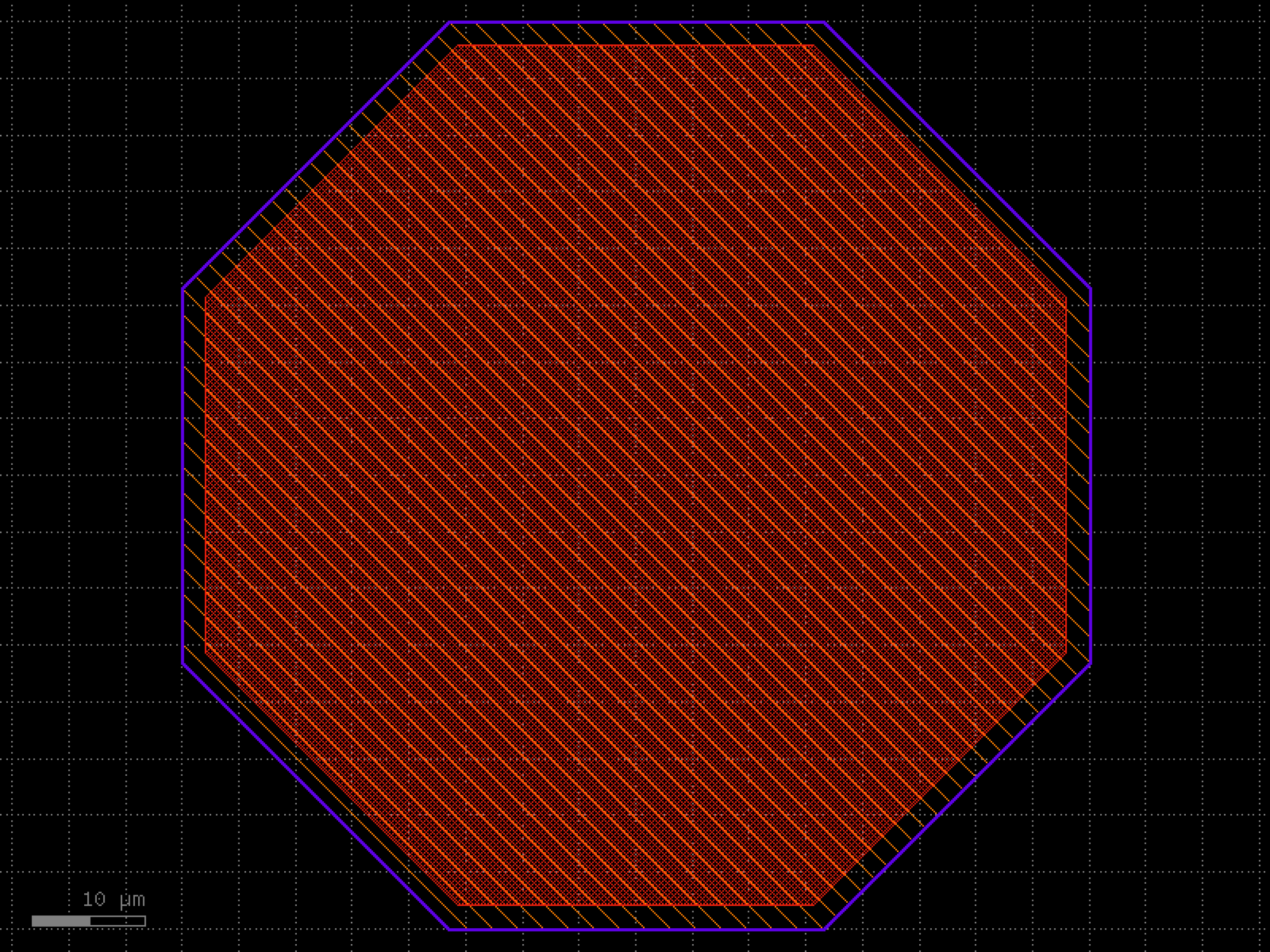
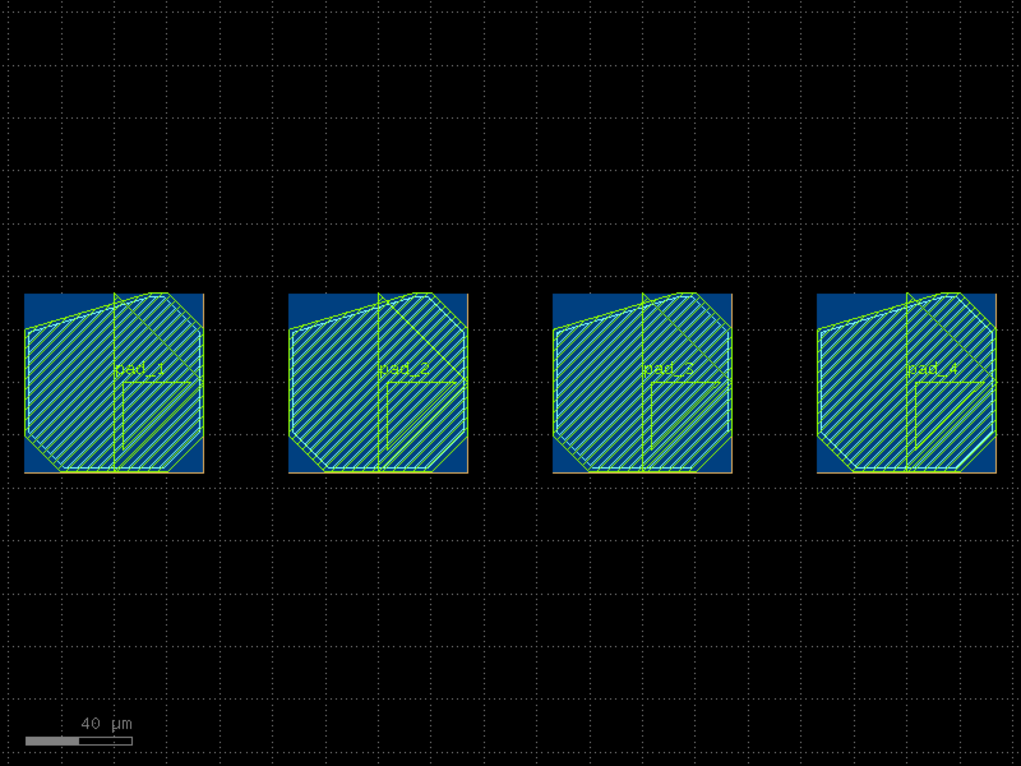
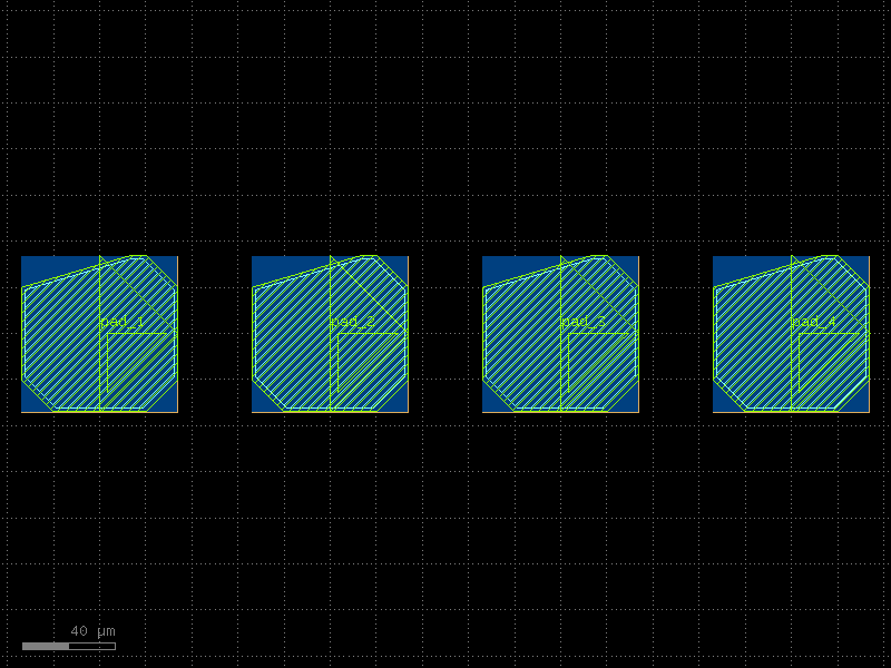
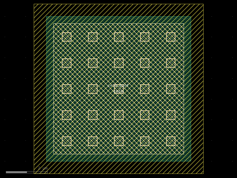
bondpad_array#
- ihp.cells.bondpad_array(n_pads=4, pad_pitch=100.0, pad_diameter=80.0, shape='octagon', layer_top_metal='TopMetal2drawing', layer_top_metal_pin='TopMetal2pin', layer_passiv='Passivpillar', layer_dfpad='dfpaddrawing', bbox_offsets=(-2.1, 0))[source]#
Create an array of bondpads.
- Parameters:
n_pads (int) – Number of bondpads.
pad_pitch (float) – Pitch between bondpad centers in micrometers.
pad_diameter (float) – Diameter of each bondpad in micrometers.
shape (Literal['octagon', 'square', 'circle']) – Shape of the bondpads.
layer_top_metal (tuple[int, int] | str | int | LayerEnum) – Top metal layer for the bondpad.
layer_passiv (tuple[int, int] | str | int | LayerEnum) – Passivation layer.
layer_dfpad (tuple[int, int] | str | int | LayerEnum) – Deep fill pad layer.
bbox_offsets (tuple[float, ...] | None) – Offsets for each additional layer.
layer_top_metal_pin (tuple[int, int] | str | int | LayerEnum)
- Returns:
Component with bondpad array.
- Return type:
Component
import warnings
warnings.filterwarnings("ignore", category=DeprecationWarning)

from ihp import PDK
from ihp import cells

PDK.activate()

c = cells.bondpad_array(n_pads=4, pad_pitch=100.0, pad_diameter=80.0, shape='octagon', layer_top_metal='TopMetal2drawing', layer_top_metal_pin='TopMetal2pin', layer_passiv='Passivpillar', layer_dfpad='dfpaddrawing', bbox_offsets=(-2.1, 0)).copy()
c.draw_ports()
c.plot()
(Source code, png, hires.png, pdf)

cmim#
- ihp.cells.cmim(width=6.0, length=6.0, layer_metal5='Metal5drawing', layer_mim='MIMdrawing', layer_vmim='Vmimdrawing', layer_topmetal1='TopMetal1drawing', layer_cap_mark='MemCapdrawing', layer_m4nofill='Metal4nofill', layer_m5nofill='Metal5nofill', layer_tm1nofill='TopMetal1nofill', layer_tm2nofill='TopMetal2nofill', layer_text='TEXTdrawing', layer_metal5label='Metal5label', layer_topmetal1label='TopMetal1label', layer_metal5pin='Metal5pin', layer_topmetal1pin='TopMetal1pin', model='cmim', **kwargs)[source]#
Create a MIM (Metal-Insulator-Metal) capacitor.
- Parameters:
width (float) – Width of the capacitor in micrometers.
length (float) – Length of the capacitor in micrometers.
bot_enclosure – Bottol Metal5 layer enclosure
top_enclosure
layer_metal5 (tuple[int, int] | str | int | LayerEnum) – Metal 5 drawing layer.
layer_mim (tuple[int, int] | str | int | LayerEnum) – MIM device drawing layer.
layer_vmim (tuple[int, int] | str | int | LayerEnum) – Vmim (MIM-TopMetal1 Via) drawing layer.
layer_topmetal1 (tuple[int, int] | str | int | LayerEnum) – TopMetal1 drawing layer.
layer_cap_mark (tuple[int, int] | str | int | LayerEnum) – MemCap drawing layer.
layer_m4nofill (tuple[int, int] | str | int | LayerEnum) – Metal4 nofill logic layer.
layer_m5nofill (tuple[int, int] | str | int | LayerEnum) – Metal5 nofill logic layer.
layer_tm1nofill (tuple[int, int] | str | int | LayerEnum) – TopMetal1 nofill logic layer.
layer_tm2nofill (tuple[int, int] | str | int | LayerEnum) – TopMetal2 nofill logic layer.
layer_text (tuple[int, int] | str | int | LayerEnum) – TEXT drawing layer.
layer_metal5label (tuple[int, int] | str | int | LayerEnum) – Metal5 label logic layer.
layer_topmetal1label (tuple[int, int] | str | int | LayerEnum) – TopMetal1 label logic layer.
layer_metal5pin (tuple[int, int] | str | int | LayerEnum) – Metal5 pin logic layer.
layer_topmetal1pin (tuple[int, int] | str | int | LayerEnum) – TopMetal1 pin logic layer.
model (str) – Device model name.
- Returns:
Component with MIM capacitor layout.
- Raises:
ValueError – If width or length is outside allowed range.
- Return type:
Component
import warnings
warnings.filterwarnings("ignore", category=DeprecationWarning)

from ihp import PDK
from ihp import cells

PDK.activate()

c = cells.cmim(width=6.0, length=6.0, layer_metal5='Metal5drawing', layer_mim='MIMdrawing', layer_vmim='Vmimdrawing', layer_topmetal1='TopMetal1drawing', layer_cap_mark='MemCapdrawing', layer_m4nofill='Metal4nofill', layer_m5nofill='Metal5nofill', layer_tm1nofill='TopMetal1nofill', layer_tm2nofill='TopMetal2nofill', layer_text='TEXTdrawing', layer_metal5label='Metal5label', layer_topmetal1label='TopMetal1label', layer_metal5pin='Metal5pin', layer_topmetal1pin='TopMetal1pin', model='cmim').copy()
c.draw_ports()
c.plot()
(Source code, png, hires.png, pdf)
cmom#
- ihp.cells.cmom(nfingers=1, length=4.0, spacing=0.26, botmetal='Metal1', topmetal='Metal3', layer_metal1='Metal1drawing', layer_metal2='Metal2drawing', layer_metal3='Metal3drawing', layer_metal4='Metal4drawing', layer_metal5='Metal5drawing', layer_metal1pin='Metal1pin', layer_metal2pin='Metal2pin', layer_metal3pin='Metal3pin', layer_metal4pin='Metal4pin', layer_metal5pin='Metal5pin', layer_metal1label='Metal1label', layer_metal2label='Metal2label', layer_metal3label='Metal3label', layer_metal4label='Metal4label', layer_metal5label='Metal5label', layer_metal1nofill='Metal1nofill', layer_metal2nofill='Metal2nofill', layer_metal3nofill='Metal3nofill', layer_metal4nofill='Metal4nofill', layer_metal5nofill='Metal5nofill', layer_cap_mark='MemCapdrawing', layer_text='TEXTdrawing', model='cmom', **kwargs)[source]#
Create a MOM (Metal-Over-Metal) interdigitated capacitor.
- Parameters:
nfingers (int) – Number of inside fingers.
length (float) – Length of the capacitor in micrometers.
spacing (float) – Spacing between top and bottom electrodes. Higher spacing, lower capacitance.
botmetal (tuple[int, int] | str | int | LayerEnum) – Bottom Metal layer for the capacitor stack.
topmetal (tuple[int, int] | str | int | LayerEnum) – Top Metal layer for the capacitor stack.
Layers (---)
layer_metal1 (tuple[int, int] | str | int | LayerEnum) – Metal1 drawing layer.
layer_metal2 (tuple[int, int] | str | int | LayerEnum) – Metal2 drawing layer.
layer_metal3 (tuple[int, int] | str | int | LayerEnum) – Metal3 drawing layer.
layer_metal4 (tuple[int, int] | str | int | LayerEnum) – Metal4 drawing layer.
layer_metal5 (tuple[int, int] | str | int | LayerEnum) – Metal5 drawing layer.
layer_metal1pin (tuple[int, int] | str | int | LayerEnum) – Metal1 pin logic layer.
layer_metal2pin (tuple[int, int] | str | int | LayerEnum) – Metal2 pin logic layer.
layer_metal3pin (tuple[int, int] | str | int | LayerEnum) – Metal3 pin logic layer.
layer_metal4pin (tuple[int, int] | str | int | LayerEnum) – Metal4 pin logic layer.
layer_metal5pin (tuple[int, int] | str | int | LayerEnum) – Metal5 pin logic layer.
layer_metal1label (tuple[int, int] | str | int | LayerEnum) – Metal1 label logic layer.
layer_metal2label (tuple[int, int] | str | int | LayerEnum) – Metal2 label logic layer.
layer_metal3label (tuple[int, int] | str | int | LayerEnum) – Metal3 label logic layer.
layer_metal4label (tuple[int, int] | str | int | LayerEnum) – Metal4 label logic layer.
layer_metal5label (tuple[int, int] | str | int | LayerEnum) – Metal5 label logic layer.
layer_metal1nofill (tuple[int, int] | str | int | LayerEnum) – Metal1 nofill logic layer.
layer_metal2nofill (tuple[int, int] | str | int | LayerEnum) – Metal2 nofill logic layer.
layer_metal3nofill (tuple[int, int] | str | int | LayerEnum) – Metal3 nofill logic layer.
layer_metal4nofill (tuple[int, int] | str | int | LayerEnum) – Metal4 nofill logic layer.
layer_metal5nofill (tuple[int, int] | str | int | LayerEnum) – Metal5 nofill logic layer.
layer_cap_mark (tuple[int, int] | str | int | LayerEnum) – MemCapdrawing logic layer.
layer_text (tuple[int, int] | str | int | LayerEnum) – TEXT drawing layer
model (str) – Device model name.
- Returns:
Component with MOM capacitor layout.
- Return type:
Component
Raises:
import warnings
warnings.filterwarnings("ignore", category=DeprecationWarning)

from ihp import PDK
from ihp import cells

PDK.activate()

c = cells.cmom(nfingers=1, length=4.0, spacing=0.26, botmetal='Metal1', topmetal='Metal3', layer_metal1='Metal1drawing', layer_metal2='Metal2drawing', layer_metal3='Metal3drawing', layer_metal4='Metal4drawing', layer_metal5='Metal5drawing', layer_metal1pin='Metal1pin', layer_metal2pin='Metal2pin', layer_metal3pin='Metal3pin', layer_metal4pin='Metal4pin', layer_metal5pin='Metal5pin', layer_metal1label='Metal1label', layer_metal2label='Metal2label', layer_metal3label='Metal3label', layer_metal4label='Metal4label', layer_metal5label='Metal5label', layer_metal1nofill='Metal1nofill', layer_metal2nofill='Metal2nofill', layer_metal3nofill='Metal3nofill', layer_metal4nofill='Metal4nofill', layer_metal5nofill='Metal5nofill', layer_cap_mark='MemCapdrawing', layer_text='TEXTdrawing', model='cmom').copy()
c.draw_ports()
c.plot()
(Source code, png, hires.png, pdf)

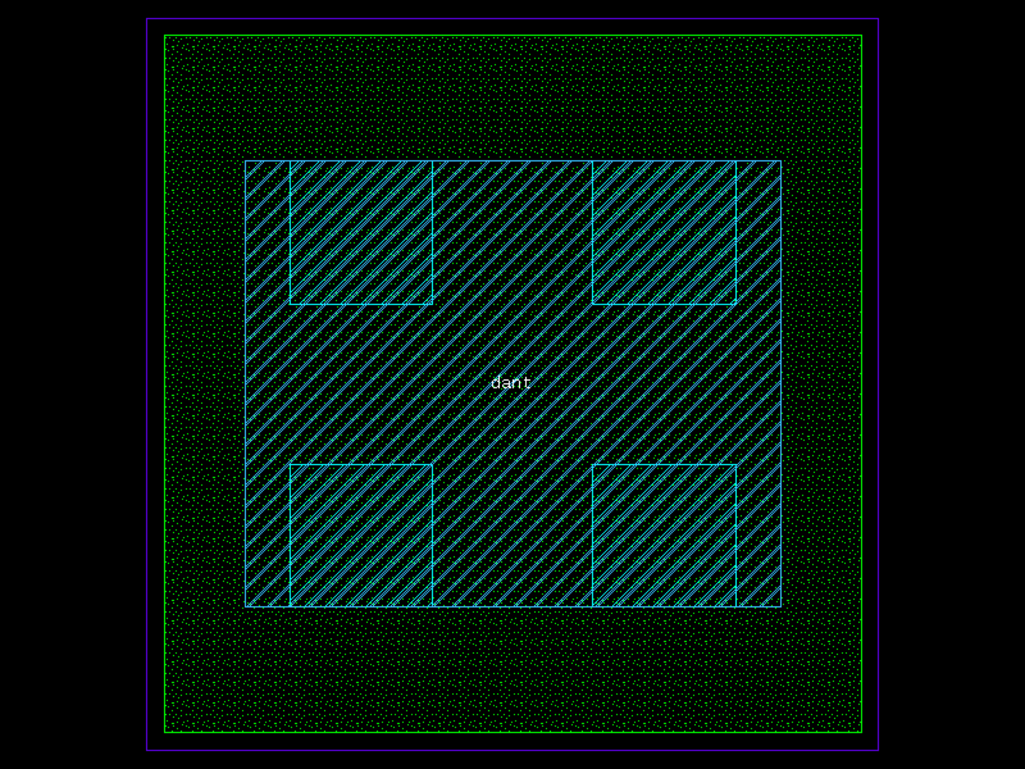
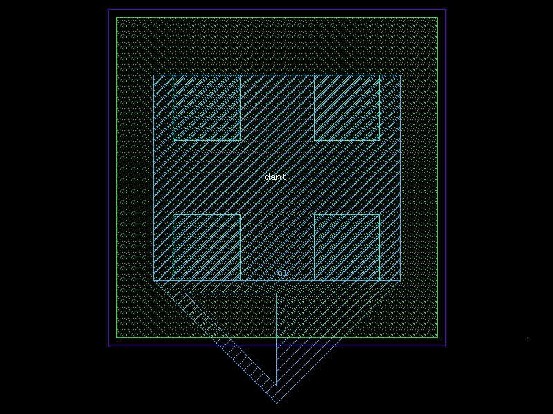
dantenna#
- ihp.cells.dantenna(width=0.78, length=0.78, addRecLayer='t', guardRingType='none', guardRingDistance=1.0)[source]#
Creates a diode antenna (dantenna) structure.
This function generates a layout cell containing a rectangular antenna region with optional recognition layers and guard ring structures. Parameters allow customization of the antenna geometry and the type and spacing of guard rings.
- Parameters:
width (float) – Width of the antenna rectangle in microns.
length (float) – Length of the antenna rectangle in microns.
addRecLayer (Literal['t', 'f']) – Recognition layer to add (e.g., ‘M1’ for metal1, ‘M2’ for metal2, or None for none).
guardRingType (Literal['none', 'psub']) – Type of guard ring to include. Options include: - ‘none’: No guard ring - ‘psub’: P-type guard ring
guardRingDistance (float) – Spacing between the antenna body and guard ring in microns.
- Returns:
The generated antenna component.
- Return type:
gdsfactory.Component
- Raises:
ValueError – If width or length is outside allowed range.
import warnings
warnings.filterwarnings("ignore", category=DeprecationWarning)

from ihp import PDK
from ihp import cells

PDK.activate()

c = cells.dantenna(width=0.78, length=0.78, addRecLayer='t', guardRingType='none', guardRingDistance=1.0).copy()
c.draw_ports()
c.plot()
(Source code, png, hires.png, pdf)

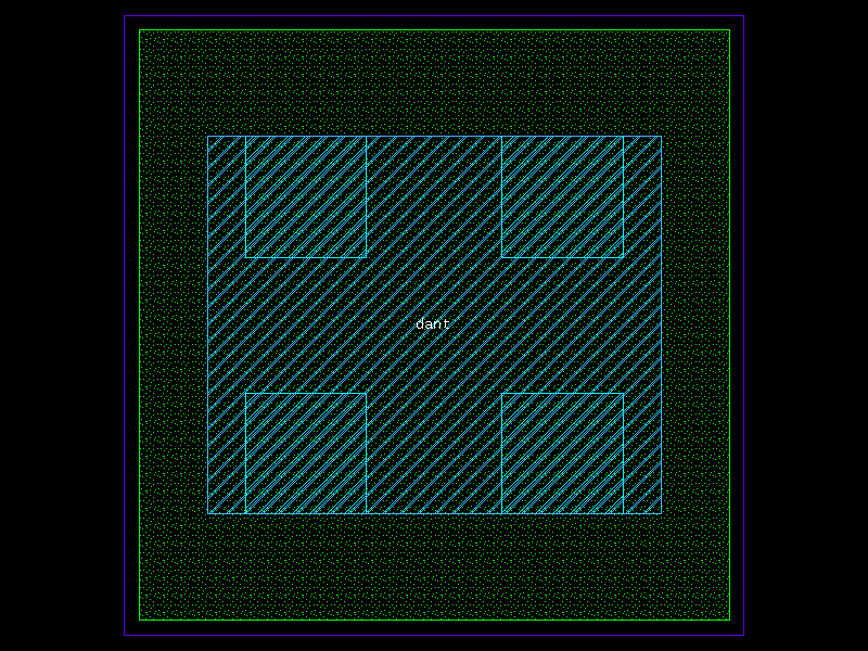
dpantenna#
- ihp.cells.dpantenna(width=0.78, length=0.78, addRecLayer='t', guardRingType='none', guardRingDistance=1.0)[source]#
Creates a dual-polarity antenna (dpantenna) structure.
Generates a layout cell containing a rectangular antenna region with an optional recognition layer and an optional n-well guard ring. Parameters allow customization of the antenna geometry and the spacing between the antenna body and the surrounding guard ring.
- Parameters:
width (float) – Width of the antenna rectangle in microns.
length (float) – Length of the antenna rectangle in microns.
addRecLayer (Literal['t', 'f']) – Whether to add a recognition layer. Valid values: - ‘t’: Add recognition layer. - ‘f’: Do not add a recognition layer.
guardRingType (Literal['none', 'nwell']) – Type of guard ring to include. Valid values: - ‘none’: No guard ring. - ‘nwell’: Surrounding n-well guard ring.
guardRingDistance (float) – Spacing between the antenna body and the n-well guard ring, in microns.
- Returns:
The generated antenna component.
- Return type:
gdsfactory.Component
- Raises:
ValueError – If width or length is outside allowed range.
import warnings
warnings.filterwarnings("ignore", category=DeprecationWarning)

from ihp import PDK
from ihp import cells

PDK.activate()

c = cells.dpantenna(width=0.78, length=0.78, addRecLayer='t', guardRingType='none', guardRingDistance=1.0).copy()
c.draw_ports()
c.plot()
(Source code, png, hires.png, pdf)

esd_nmos#
- ihp.cells.esd_nmos(width=50.0, length=0.5, nf=10, model='nmoscl_2', layer_pwell='PWelldrawing', layer_activ='Activdrawing', layer_gatpoly='GatPolydrawing', layer_nsd='nSDdrawing', layer_cont='Contdrawing', layer_metal1='Metal1drawing', layer_metal1_pin='Metal1pin', layer_metal2='Metal2drawing', layer_metal2_pin='Metal2pin', layer_esd='Recogesd')[source]#
Create an ESD protection NMOS device.
- Parameters:
width (float) – Total width of the ESD device in micrometers.
length (float) – Gate length in micrometers.
nf (int) – Number of fingers.
model (str) – Device model name.
layer_pwell (tuple[int, int] | str | int | LayerEnum) – P-well layer.
layer_activ (tuple[int, int] | str | int | LayerEnum) – Active region layer.
layer_gatpoly (tuple[int, int] | str | int | LayerEnum) – Gate polysilicon layer.
layer_nsd (tuple[int, int] | str | int | LayerEnum) – N+ source/drain doping layer.
layer_cont (tuple[int, int] | str | int | LayerEnum) – Contact layer.
layer_metal1 (tuple[int, int] | str | int | LayerEnum) – Metal1 layer.
layer_metal2 (tuple[int, int] | str | int | LayerEnum) – Metal2 layer.
layer_esd (tuple[int, int] | str | int | LayerEnum) – ESD marker layer.
layer_metal1_pin (tuple[int, int] | str | int | LayerEnum)
layer_metal2_pin (tuple[int, int] | str | int | LayerEnum)
- Returns:
Component with ESD NMOS layout.
- Return type:
Component
import warnings
warnings.filterwarnings("ignore", category=DeprecationWarning)

from ihp import PDK
from ihp import cells

PDK.activate()

c = cells.esd_nmos(width=50.0, length=0.5, nf=10, model='nmoscl_2', layer_pwell='PWelldrawing', layer_activ='Activdrawing', layer_gatpoly='GatPolydrawing', layer_nsd='nSDdrawing', layer_cont='Contdrawing', layer_metal1='Metal1drawing', layer_metal1_pin='Metal1pin', layer_metal2='Metal2drawing', layer_metal2_pin='Metal2pin', layer_esd='Recogesd').copy()
c.draw_ports()
c.plot()
(Source code, png, hires.png, pdf)

guard_ring#
- ihp.cells.guard_ring(width=0.5, guardRingSpacing=0.14, guardRingType='psub', bbox=None, path=None, layer_activ='Activdrawing', layer_cont='Contdrawing', layer_metal1='Metal1drawing', layer_psd='pSDdrawing', layer_nwell='NWelldrawing', layer_nsd='nSDdrawing', **kwargs)[source]#
Create an N-Well (NW) and N-Plus (NP) or a P-Plus (PP) guard ring around a boundary box, or, if bbox is not provided, along a provided path of points.
- Parameters:
width (float) – Width of the guard ring group path, defining the width of the Metal1 Path.
guardRingSpacing (float) – Spacing between the Metal1 Path and the component BBox.
guardRingType (Literal['psub', 'nwell']) – Literal[“psub”, ‘nwell’] Type of Guard-Ring (NP = nwell or PP = psub).
bbox (tuple[tuple[float32 | float64 | float, float32 | float64 | float], tuple[float32 | float64 | float, float32 | float64 | float]] | None) – Encapsulated component bounding box.
path (list[tuple[tuple[float32 | float64 | float, float32 | float64 | float], tuple[float32 | float64 | float, float32 | float64 | float]]] | None) – Path point for the group path defining the Guard Ring,
layer_activ (tuple[int, int] | str | int | LayerEnum) – Activ drawing layer.
layer_cont (tuple[int, int] | str | int | LayerEnum) – Contact Via drawing layer.
layer_metal1 (tuple[int, int] | str | int | LayerEnum) – Metal1 drawing layer.
layer_psd (tuple[int, int] | str | int | LayerEnum) – pSD / P-Plus drawing layer.
layer_nwell (tuple[int, int] | str | int | LayerEnum) – NWell drawing layer.
layer_nsd (tuple[int, int] | str | int | LayerEnum) – nSD / N-Plus drawing layer.
- Returns:
c - Component containing the Guard-Ring group path.
- Return type:
Component
Raises:
import warnings
warnings.filterwarnings("ignore", category=DeprecationWarning)

from ihp import PDK
from ihp import cells

PDK.activate()

c = cells.guard_ring(width=0.5, guardRingSpacing=0.14, guardRingType='psub', layer_activ='Activdrawing', layer_cont='Contdrawing', layer_metal1='Metal1drawing', layer_psd='pSDdrawing', layer_nwell='NWelldrawing', layer_nsd='nSDdrawing').copy()
c.draw_ports()
c.plot()
inductor2#
- ihp.cells.inductor2(width=2.0, space=2.1, diameter=25.35, vias_width=0.9, resistance=0.5777, inductance=3.3303e-11, terminal_1_length=30.0, turns=1, layer_metal_1='TopMetal1drawing', layer_metal_2='TopMetal2drawing', layer_inductor='INDdrawing', layer_metal_1_pin='TopMetal1pin', layer_metal_2_pin='TopMetal2pin', layer_ind_pin='INDpin', layer_via='TopVia2drawing', layers_no_fill=('Activnofill', 'GatPolynofill', 'Metal1nofill', 'Metal2nofill', 'Metal3nofill', 'Metal4nofill', 'Metal5nofill', 'TopMetal1nofill', 'TopMetal2nofill', 'PWellblock', 'NoRCXdrawing'))[source]#
Create a 2-turn inductor.
- Parameters:
width (float) – Width of the inductor trace in micrometers.
space (float) – Space between turns in micrometers.
diameter (float) – Inner diameter in micrometers.
vias_width (float) – Width of vias in micrometers (only when turns > 2)
resistance (float) – Resistance in ohms.
inductance (float) – Inductance in henries.
terminal_1_length (float) – Length of the shorter terminal
turns (int) – Number of turns (default 1 for inductor2).
layer_metal_1 (tuple[int, int] | str | int | LayerEnum)
layer_metal_2 (tuple[int, int] | str | int | LayerEnum)
layer_inductor (tuple[int, int] | str | int | LayerEnum)
layer_metal_1_pin (tuple[int, int] | str | int | LayerEnum)
layer_metal_2_pin (tuple[int, int] | str | int | LayerEnum)
layer_ind_pin (tuple[int, int] | str | int | LayerEnum)
layer_via (tuple[int, int] | str | int | LayerEnum)
layers_no_fill (Sequence[tuple[int, int] | str | int | LayerEnum])
- Returns:
Component with inductor layout.
- Return type:
Component
import warnings
warnings.filterwarnings("ignore", category=DeprecationWarning)

from ihp import PDK
from ihp import cells

PDK.activate()

c = cells.inductor2(width=2.0, space=2.1, diameter=25.35, vias_width=0.9, resistance=0.5777, inductance=3.3303e-11, terminal_1_length=30.0, turns=1, layer_metal_1='TopMetal1drawing', layer_metal_2='TopMetal2drawing', layer_inductor='INDdrawing', layer_metal_1_pin='TopMetal1pin', layer_metal_2_pin='TopMetal2pin', layer_ind_pin='INDpin', layer_via='TopVia2drawing', layers_no_fill=('Activnofill', 'GatPolynofill', 'Metal1nofill', 'Metal2nofill', 'Metal3nofill', 'Metal4nofill', 'Metal5nofill', 'TopMetal1nofill', 'TopMetal2nofill', 'PWellblock', 'NoRCXdrawing')).copy()
c.draw_ports()
c.plot()
(Source code, png, hires.png, pdf)

inductor3#
- ihp.cells.inductor3(width=2.0, space=2.1, diameter=25.84, vias_width=0.9, resistance=1.386, inductance=2.215e-10, terminal_1_length=30.0, turns=2, layer_metal_1='TopMetal1drawing', layer_metal_2='TopMetal2drawing', layer_inductor='INDdrawing', layer_metal_1_pin='TopMetal1pin', layer_metal_2_pin='TopMetal2pin', layer_ind_pin='INDpin', layer_via='TopVia2drawing', layers_no_fill=('Activnofill', 'GatPolynofill', 'Metal1nofill', 'Metal2nofill', 'Metal3nofill', 'Metal4nofill', 'Metal5nofill', 'TopMetal1nofill', 'TopMetal2nofill', 'PWellblock', 'NoRCXdrawing'))[source]#
Create a 3-turn inductor.
- Parameters:
width (float) – Width of the inductor trace in micrometers.
space (float) – Space between turns in micrometers.
diameter (float) – Inner diameter in micrometers.
vias_width (float) – Width of vias in micrometers (only when turns > 2)
resistance (float) – Resistance in ohms.
inductance (float) – Inductance in henries.
terminal_1_length (float) – Length of the shorter terminal
turns (int) – Number of turns (default 2 for inductor3).
layer_metal_1 (tuple[int, int] | str | int | LayerEnum)
layer_metal_2 (tuple[int, int] | str | int | LayerEnum)
layer_inductor (tuple[int, int] | str | int | LayerEnum)
layer_metal_1_pin (tuple[int, int] | str | int | LayerEnum)
layer_metal_2_pin (tuple[int, int] | str | int | LayerEnum)
layer_ind_pin (tuple[int, int] | str | int | LayerEnum)
layer_via (tuple[int, int] | str | int | LayerEnum)
layers_no_fill (Sequence[tuple[int, int] | str | int | LayerEnum])
- Returns:
Component with inductor layout.
- Return type:
Component
import warnings
warnings.filterwarnings("ignore", category=DeprecationWarning)

from ihp import PDK
from ihp import cells

PDK.activate()

c = cells.inductor3(width=2.0, space=2.1, diameter=25.84, vias_width=0.9, resistance=1.386, inductance=2.215e-10, terminal_1_length=30.0, turns=2, layer_metal_1='TopMetal1drawing', layer_metal_2='TopMetal2drawing', layer_inductor='INDdrawing', layer_metal_1_pin='TopMetal1pin', layer_metal_2_pin='TopMetal2pin', layer_ind_pin='INDpin', layer_via='TopVia2drawing', layers_no_fill=('Activnofill', 'GatPolynofill', 'Metal1nofill', 'Metal2nofill', 'Metal3nofill', 'Metal4nofill', 'Metal5nofill', 'TopMetal1nofill', 'TopMetal2nofill', 'PWellblock', 'NoRCXdrawing')).copy()
c.draw_ports()
c.plot()
(Source code, png, hires.png, pdf)

nmos#
- ihp.cells.nmos(width=0.15, length=0.13, nf=1, m=1, model='sg13_lv_nmos')[source]#
Create an NMOS transistor.
- Parameters:
width (float) – Total width of the transistor in micrometers.
length (float) – Gate length in micrometers.
nf (int) – Number of fingers.
m (int) – Multiplier (number of parallel devices).
model (str) – Device model name.
- Returns:
Component with NMOS transistor layout.
- Raises:
ValueError – If width, length, or nf is outside allowed range.
- Return type:
Component
import warnings
warnings.filterwarnings("ignore", category=DeprecationWarning)

from ihp import PDK
from ihp import cells

PDK.activate()

c = cells.nmos(width=0.15, length=0.13, nf=1, m=1, model='sg13_lv_nmos').copy()
c.draw_ports()
c.plot()
(Source code, png, hires.png, pdf)
nmos_hv#
- ihp.cells.nmos_hv(width=0.6, length=0.45, nf=1, m=1, model='sg13_hv_nmos')[source]#
Create a high-voltage NMOS transistor.
- Parameters:
width (float) – Total width of the transistor in micrometers.
length (float) – Gate length in micrometers.
nf (int) – Number of fingers.
m (int) – Multiplier (number of parallel devices).
model (str) – Device model name.
- Returns:
Component with HV NMOS transistor layout.
- Raises:
ValueError – If width, length, or nf is outside allowed range.
- Return type:
Component
import warnings
warnings.filterwarnings("ignore", category=DeprecationWarning)

from ihp import PDK
from ihp import cells

PDK.activate()

c = cells.nmos_hv(width=0.6, length=0.45, nf=1, m=1, model='sg13_hv_nmos').copy()
c.draw_ports()
c.plot()
(Source code, png, hires.png, pdf)
npn13G2#
- ihp.cells.npn13G2(baspolyx=0.3, bipwinx=0.07, bipwiny=0.1, empolyx=0.15, empolyy=0.18, STI=0.44, emitter_length=0.9, emitter_width=0.7, Nx=1, Ny=1, text='npn13G2', CMetY1=0, CMetY2=0)[source]#
Returns the IHP npn13G2 BJT transistor as a gdsfactory Component.
- Parameters:
Nx (int) – Number of emitter fingers in the x-direction.
Ny (int) – Number of emitter fingers in the y-direction.
emitter_length (float) – Length of the emitter region in microns.
emitter_width (float) – Width of the emitter region in microns.
STI (float) – Shallow Trench Isolation width in microns.
baspolyx (float) – Base poly extension in x-direction in microns.
bipwinx (float) – Bipolar window extension in x-direction in microns.
bipwiny (float) – Bipolar window extension in y-direction in microns.
empolyx (float) – Emitter poly extension in x-direction in microns.
empolyy (float) – Emitter poly extension in y-direction in microns.
text (str) – Text label for the transistor.
CMetY1 (float) – Contact metal Y1 dimension in microns.
CMetY2 (float) – Contact metal Y2 dimension in microns.
- Returns:
The generated npn13G2 transistor layout.
- Return type:
gdsfactory.Component
- Raises:
ValueError – If finger count is outside allowed range.
import warnings
warnings.filterwarnings("ignore", category=DeprecationWarning)

from ihp import PDK
from ihp import cells

PDK.activate()

c = cells.npn13G2(baspolyx=0.3, bipwinx=0.07, bipwiny=0.1, empolyx=0.15, empolyy=0.18, STI=0.44, emitter_length=0.9, emitter_width=0.7, Nx=1, Ny=1, text='npn13G2', CMetY1=0, CMetY2=0).copy()
c.draw_ports()
c.plot()
(Source code, png, hires.png, pdf)

npn13G2L#
- ihp.cells.npn13G2L(emitter_length=1, emitter_width=0.07, Nx=1)[source]#
Builds the IHP npn13G2L BJT transistor as a gdsfactory Component.
The transistor geometry is defined by the number of emitter fingers and the dimensions of each emitter finger.
- Parameters:
emitter_length (float) – Length of each emitter finger, in microns.
emitter_width (float) – Width of each emitter finger, in microns.
Nx (int) – Number of emitter fingers.
- Returns:
The generated npn13G2L transistor layout.
- Return type:
gdsfactory.Component
- Raises:
ValueError – If finger count is outside allowed range.
import warnings
warnings.filterwarnings("ignore", category=DeprecationWarning)

from ihp import PDK
from ihp import cells

PDK.activate()

c = cells.npn13G2L(emitter_length=1, emitter_width=0.07, Nx=1).copy()
c.draw_ports()
c.plot()
(Source code, png, hires.png, pdf)

npn13G2V#
- ihp.cells.npn13G2V(emitter_length=1, emitter_width=0.12, Nx=1)[source]#
Builds the IHP npn13G2V BJT transistor as a gdsfactory Component.
The transistor geometry is defined by the number of emitter fingers and the dimensions of each emitter finger.
- Parameters:
emitter_length (float) – Length of each emitter finger, in microns.
emitter_width (float) – Width of each emitter finger, in microns.
Nx (int) – Number of emitter fingers.
- Returns:
The generated npn13G2V transistor layout.
- Return type:
gdsfactory.Component
- Raises:
ValueError – If finger count is outside allowed range.
import warnings
warnings.filterwarnings("ignore", category=DeprecationWarning)

from ihp import PDK
from ihp import cells

PDK.activate()

c = cells.npn13G2V(emitter_length=1, emitter_width=0.12, Nx=1).copy()
c.draw_ports()
c.plot()
(Source code, png, hires.png, pdf)

ntap1#
- ihp.cells.ntap1(width=1.0, length=1.0, rows=1, cols=1, layer_nwell='NWelldrawing', layer_activ='Activdrawing', layer_nsd='nSDdrawing', layer_cont='Contdrawing', layer_metal1='Metal1drawing', layer_metal1_pin='Metal1pin')[source]#
Create an N+ substrate tap.
- Parameters:
width (float) – Width of the tap in micrometers.
length (float) – Length of the tap in micrometers.
rows (int) – Number of contact rows.
cols (int) – Number of contact columns.
layer_nwell (tuple[int, int] | str | int | LayerEnum) – N-well layer.
layer_activ (tuple[int, int] | str | int | LayerEnum) – Active region layer.
layer_nsd (tuple[int, int] | str | int | LayerEnum) – N+ source/drain doping layer.
layer_cont (tuple[int, int] | str | int | LayerEnum) – Contact layer.
layer_metal1 (tuple[int, int] | str | int | LayerEnum) – Metal1 layer.
layer_metal1_pin (tuple[int, int] | str | int | LayerEnum)
- Returns:
Component with N+ tap layout.
- Raises:
ValueError – If width or length is outside allowed range.
- Return type:
Component
import warnings
warnings.filterwarnings("ignore", category=DeprecationWarning)

from ihp import PDK
from ihp import cells

PDK.activate()

c = cells.ntap1(width=1.0, length=1.0, rows=1, cols=1, layer_nwell='NWelldrawing', layer_activ='Activdrawing', layer_nsd='nSDdrawing', layer_cont='Contdrawing', layer_metal1='Metal1drawing', layer_metal1_pin='Metal1pin').copy()
c.draw_ports()
c.plot()
(Source code, png, hires.png, pdf)

pack_doe#
- ihp.cells.pack_doe(doe, settings, do_permutations=False, function=None, **kwargs)[source]#
Packs a component DOE (Design of Experiment) using pack.
- Parameters:
doe (str | Callable[[...], Component] | dict[str, Any] | DKCell | partial[Component]) – function to return Components.
settings (dict[str, tuple[Any, ...]]) – component settings.
do_permutations (bool) – for each setting.
function (str | Callable[[...], Component] | dict[str, Any] | None) – to apply (add padding, grating couplers).
kwargs – for pack.
- Keyword Arguments:
spacing – Minimum distance between adjacent shapes.
aspect_ratio – (width, height) ratio of the rectangular bin.
max_size – Limits the size into which the shapes will be packed.
sort_by_area – Pre-sorts the shapes by area.
density – Values closer to 1 pack tighter but require more computation.
precision – Desired precision for rounding vertex coordinates.
text – Optional function to add text labels.
text_prefix – for labels. For example. ‘A’ for ‘A1’, ‘A2’…
text_offsets – relative to component size info anchor. Defaults to center.
text_anchors – relative to component (ce cw nc ne nw sc se sw center cc).
name_prefix – for each packed component (avoids the Unnamed cells warning). Note that the suffix contains a uuid so the name will not be deterministic.
rotation – for each component in degrees.
h_mirror – horizontal mirror in y axis (x, 1) (1, 0). This is the most common.
v_mirror – vertical mirror using x axis (1, y) (0, y).
- Return type:
Component
import warnings
warnings.filterwarnings("ignore", category=DeprecationWarning)

from ihp import PDK
from ihp import cells

PDK.activate()

c = cells.pack_doe(do_permutations=False).copy()
c.draw_ports()
c.plot()
pack_doe_grid#
- ihp.cells.pack_doe_grid(doe, settings, do_permutations=False, function=None, with_text=False, **kwargs)[source]#
Packs a component DOE (Design of Experiment) using grid.
- Parameters:
doe (str | Callable[[...], Component] | dict[str, Any] | DKCell | partial[Component]) – function to return Components.
settings (dict[str, tuple[Any, ...]]) – component settings.
do_permutations (bool) – for each setting.
function (str | Callable[[...], Component] | dict[str, Any] | None) – to apply to component (add padding, grating couplers).
with_text (bool) – includes text label.
kwargs – for grid.
- Keyword Arguments:
spacing – between adjacent elements on the grid, can be a tuple for different distances in height and width.
separation – If True, guarantees elements are separated with fixed spacing if False, elements are spaced evenly along a grid.
shape – x, y shape of the grid (see np.reshape). If no shape and the list is 1D, if np.reshape were run with (1, -1).
align_x – {‘x’, ‘xmin’, ‘xmax’} for x (column) alignment along.
align_y – {‘y’, ‘ymin’, ‘ymax’} for y (row) alignment along.
edge_x – {‘x’, ‘xmin’, ‘xmax’} for x (column) (ignored if separation = True).
edge_y – {‘y’, ‘ymin’, ‘ymax’} for y (row) (ignored if separation = True).
rotation – for each component in degrees.
h_mirror – horizontal mirror y axis (x, 1) (1, 0). most common mirror.
v_mirror – vertical mirror using x axis (1, y) (0, y).
- Return type:
Component
import warnings
warnings.filterwarnings("ignore", category=DeprecationWarning)

from ihp import PDK
from ihp import cells

PDK.activate()

c = cells.pack_doe_grid(do_permutations=False, with_text=False).copy()
c.draw_ports()
c.plot()
pmos#
- ihp.cells.pmos(width=0.15, length=0.13, nf=1, m=1, model='sg13_lv_pmos')[source]#
Create a PMOS transistor.
- Parameters:
width (float) – Total width of the transistor in micrometers.
length (float) – Gate length in micrometers.
nf (int) – Number of fingers.
m (int) – Multiplier (number of parallel devices).
model (str) – Device model name.
- Returns:
Component with PMOS transistor layout.
- Raises:
ValueError – If width, length, or nf is outside allowed range.
- Return type:
Component
import warnings
warnings.filterwarnings("ignore", category=DeprecationWarning)

from ihp import PDK
from ihp import cells

PDK.activate()

c = cells.pmos(width=0.15, length=0.13, nf=1, m=1, model='sg13_lv_pmos').copy()
c.draw_ports()
c.plot()
(Source code, png, hires.png, pdf)

pmos_hv#
- ihp.cells.pmos_hv(width=0.3, length=0.4, nf=1, m=1, model='sg13_hv_pmos')[source]#
Create a high-voltage PMOS transistor.
- Parameters:
width (float) – Total width of the transistor in micrometers.
length (float) – Gate length in micrometers.
nf (int) – Number of fingers.
m (int) – Multiplier (number of parallel devices).
model (str) – Device model name.
- Returns:
Component with HV PMOS transistor layout.
- Raises:
ValueError – If width, length, or nf is outside allowed range.
- Return type:
Component
import warnings
warnings.filterwarnings("ignore", category=DeprecationWarning)

from ihp import PDK
from ihp import cells

PDK.activate()

c = cells.pmos_hv(width=0.3, length=0.4, nf=1, m=1, model='sg13_hv_pmos').copy()
c.draw_ports()
c.plot()
(Source code, png, hires.png, pdf)

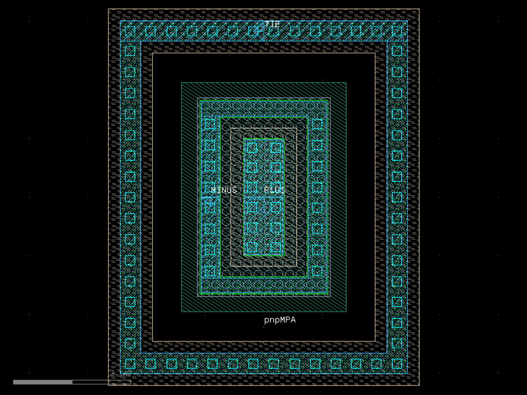
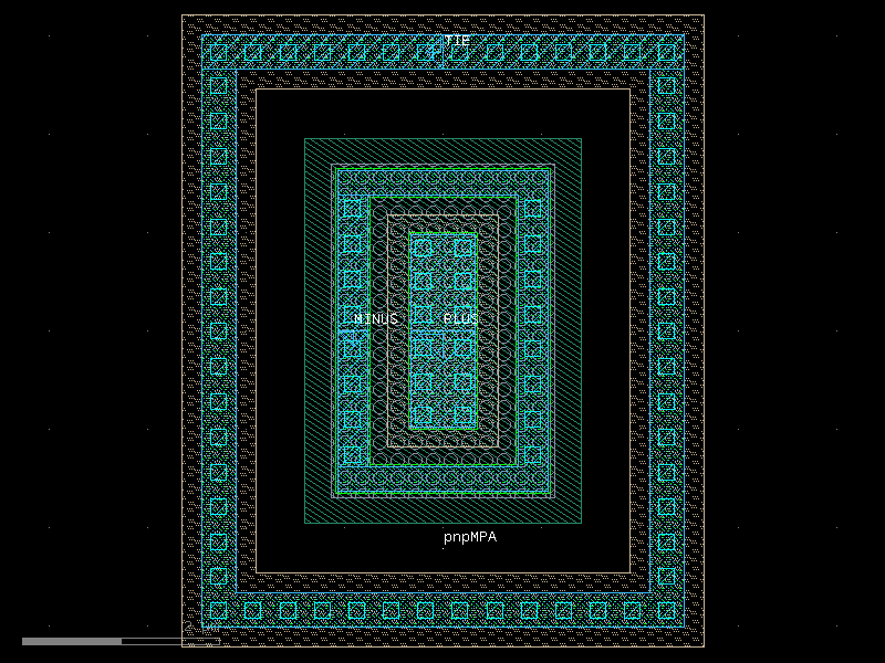
pnpMPA#
- ihp.cells.pnpMPA(length=2, width=0.7)[source]#
Returns the IHP pnpMPA BJT transistor as a gdsfactory Component.
This function generates a layout for a PNP transistor using the IHP process. The geometry of the transistor is defined by its width and length.
- Parameters:
length (float) – Length of the transistor, in microns.
width (float) – Width of the transistor, in microns.
- Returns:
The generated pnpMPA transistor layout.
- Return type:
gdsfactory.Component
- Raises:
ValueError – If width or length is outside allowed range.
import warnings
warnings.filterwarnings("ignore", category=DeprecationWarning)

from ihp import PDK
from ihp import cells

PDK.activate()

c = cells.pnpMPA(length=2, width=0.7).copy()
c.draw_ports()
c.plot()
(Source code, png, hires.png, pdf)
ptap1#
- ihp.cells.ptap1(width=1.0, length=1.0, rows=1, cols=1, layer_activ='Activdrawing', layer_psd='pSDdrawing', layer_cont='Contdrawing', layer_metal1='Metal1drawing', layer_metal1_pin='Metal1pin')[source]#
Create a P+ substrate tap.
- Parameters:
width (float) – Width of the tap in micrometers.
length (float) – Length of the tap in micrometers.
rows (int) – Number of contact rows.
cols (int) – Number of contact columns.
layer_activ (tuple[int, int] | str | int | LayerEnum) – Active region layer.
layer_psd (tuple[int, int] | str | int | LayerEnum) – P+ source/drain doping layer.
layer_cont (tuple[int, int] | str | int | LayerEnum) – Contact layer.
layer_metal1 (tuple[int, int] | str | int | LayerEnum) – Metal1 layer.
layer_metal1_pin (tuple[int, int] | str | int | LayerEnum)
- Returns:
Component with P+ tap layout.
- Raises:
ValueError – If width or length is outside allowed range.
- Return type:
Component
import warnings
warnings.filterwarnings("ignore", category=DeprecationWarning)

from ihp import PDK
from ihp import cells

PDK.activate()

c = cells.ptap1(width=1.0, length=1.0, rows=1, cols=1, layer_activ='Activdrawing', layer_psd='pSDdrawing', layer_cont='Contdrawing', layer_metal1='Metal1drawing', layer_metal1_pin='Metal1pin').copy()
c.draw_ports()
c.plot()
(Source code, png, hires.png, pdf)
rfcmim#
- ihp.cells.rfcmim(width=7.0, length=7.0, layer_pwellblock='PWellblock', layer_metal5='Metal5drawing', layer_mim='MIMdrawing', layer_vmim='Vmimdrawing', layer_topmetal1='TopMetal1drawing', layer_cap_mark='MemCapdrawing', layer_m4nofill='Metal4nofill', layer_m5nofill='Metal5nofill', layer_tm1nofill='TopMetal1nofill', layer_tm2nofill='TopMetal2nofill', layer_activ='Activdrawing', layer_cont='Contdrawing', layer_metal1='Metal1drawing', layer_psd='pSDdrawing', layer_activnoqrc='Activnoqrc', layer_metal1noqrc='Metal1noqrc', layer_metal2noqrc='Metal2noqrc', layer_metal3noqrc='Metal3noqrc', layer_metal4noqrc='Metal4noqrc', layer_metal5noqrc='Metal5noqrc', layer_topmetal1noqrc='TopMetal1noqrc', layer_text='TEXTdrawing', layer_metal1pin='Metal1pin', layer_metal5pin='Metal5pin', layer_topmetal1pin='TopMetal1pin', layer_metal5label='Metal5label', layer_topmetal1label='TopMetal1label', layer_metal1label='Metal1label', model='rfcmim')[source]#
Create a MIM (Metal-Insulator-Metal) capacitor isolated by a bulk charge-drift encapsulation P-Plus guard-ring.
- Parameters:
width (float) – Width of the capacitor in micrometers.
length (float) – Length of the capacitor in micrometers.
layer_metal5 (tuple[int, int] | str | int | LayerEnum) – Metal 5 drawing layer.
layer_mim (tuple[int, int] | str | int | LayerEnum) – MIM device drawing layer.
layer_vmim (tuple[int, int] | str | int | LayerEnum) – Vmim (MIM-TopMetal1 Via) drawing layer.
layer_topmetal1 (tuple[int, int] | str | int | LayerEnum) – TopMetal1 drawing layer.
layer_cap_mark (tuple[int, int] | str | int | LayerEnum) – MemCap drawing layer.
layer_m4nofill (tuple[int, int] | str | int | LayerEnum) – Metal4 nofill logic layer.
layer_m5nofill (tuple[int, int] | str | int | LayerEnum) – Metal5 nofill logic layer.
layer_tm1nofill (tuple[int, int] | str | int | LayerEnum) – TopMetal1 nofill logic layer.
layer_tm2nofill (tuple[int, int] | str | int | LayerEnum) – TopMetal2 nofill logic layer.
layer_text (tuple[int, int] | str | int | LayerEnum) – TEXT drawing layer.
layer_metal5label (tuple[int, int] | str | int | LayerEnum) – Metal5 label logic layer.
layer_topmetal1label (tuple[int, int] | str | int | LayerEnum) – TopMetal1 label logic layer.
layer_metal5pin (tuple[int, int] | str | int | LayerEnum) – Metal5 pin logic layer.
layer_topmetal1pin (tuple[int, int] | str | int | LayerEnum) – TopMetal1 pin logic layer.
model (str) – Device model name.
layer_pwellblock (tuple[int, int] | str | int | LayerEnum)
layer_activ (tuple[int, int] | str | int | LayerEnum)
layer_cont (tuple[int, int] | str | int | LayerEnum)
layer_metal1 (tuple[int, int] | str | int | LayerEnum)
layer_psd (tuple[int, int] | str | int | LayerEnum)
layer_activnoqrc (tuple[int, int] | str | int | LayerEnum)
layer_metal1noqrc (tuple[int, int] | str | int | LayerEnum)
layer_metal2noqrc (tuple[int, int] | str | int | LayerEnum)
layer_metal3noqrc (tuple[int, int] | str | int | LayerEnum)
layer_metal4noqrc (tuple[int, int] | str | int | LayerEnum)
layer_metal5noqrc (tuple[int, int] | str | int | LayerEnum)
layer_topmetal1noqrc (tuple[int, int] | str | int | LayerEnum)
layer_metal1pin (tuple[int, int] | str | int | LayerEnum)
layer_metal1label (tuple[int, int] | str | int | LayerEnum)
- Returns:
Component with MIM capacitor layout.
- Raises:
ValueError – If width or length is outside allowed range.
- Return type:
Component
import warnings
warnings.filterwarnings("ignore", category=DeprecationWarning)

from ihp import PDK
from ihp import cells

PDK.activate()

c = cells.rfcmim(width=7.0, length=7.0, layer_pwellblock='PWellblock', layer_metal5='Metal5drawing', layer_mim='MIMdrawing', layer_vmim='Vmimdrawing', layer_topmetal1='TopMetal1drawing', layer_cap_mark='MemCapdrawing', layer_m4nofill='Metal4nofill', layer_m5nofill='Metal5nofill', layer_tm1nofill='TopMetal1nofill', layer_tm2nofill='TopMetal2nofill', layer_activ='Activdrawing', layer_cont='Contdrawing', layer_metal1='Metal1drawing', layer_psd='pSDdrawing', layer_activnoqrc='Activnoqrc', layer_metal1noqrc='Metal1noqrc', layer_metal2noqrc='Metal2noqrc', layer_metal3noqrc='Metal3noqrc', layer_metal4noqrc='Metal4noqrc', layer_metal5noqrc='Metal5noqrc', layer_topmetal1noqrc='TopMetal1noqrc', layer_text='TEXTdrawing', layer_metal1pin='Metal1pin', layer_metal5pin='Metal5pin', layer_topmetal1pin='TopMetal1pin', layer_metal5label='Metal5label', layer_topmetal1label='TopMetal1label', layer_metal1label='Metal1label', model='rfcmim').copy()
c.draw_ports()
c.plot()
(Source code, png, hires.png, pdf)
rfnmos#
- ihp.cells.rfnmos(width=1.0, length=0.13, nf=1, m=1, cnt_rows=1, met2_cont=True, gat_ring=True, guard_ring='Yes', model='sg13_lv_nmos')[source]#
Create an RF NMOS transistor.
- Parameters:
width (float) – Total width of the transistor in micrometers.
length (float) – Gate length in micrometers.
nf (int) – Number of fingers.
m (int) – Multiplier (number of parallel devices).
cnt_rows (int) – Number of contact rows.
met2_cont (bool) – Include Metal2-to-contact connections.
gat_ring (bool) – Include gate ring around the transistor.
guard_ring (str) – Guard ring type: “Yes”, “No”, “U”, or “Top+Bottom”.
model (str) – Device model name.
- Returns:
Component with RF NMOS transistor layout.
- Raises:
ValueError – If width, length, or nf is outside allowed range.
- Return type:
Component
import warnings
warnings.filterwarnings("ignore", category=DeprecationWarning)

from ihp import PDK
from ihp import cells

PDK.activate()

c = cells.rfnmos(width=1.0, length=0.13, nf=1, m=1, cnt_rows=1, met2_cont=True, gat_ring=True, guard_ring='Yes', model='sg13_lv_nmos').copy()
c.draw_ports()
c.plot()
(Source code, png, hires.png, pdf)

rfnmos_hv#
- ihp.cells.rfnmos_hv(width=1.0, length=0.45, nf=1, m=1, cnt_rows=1, met2_cont=True, gat_ring=True, guard_ring='Yes', model='sg13_hv_nmos')[source]#
Create a high-voltage RF NMOS transistor.
- Parameters:
width (float) – Total width of the transistor in micrometers.
length (float) – Gate length in micrometers.
nf (int) – Number of fingers.
m (int) – Multiplier (number of parallel devices).
cnt_rows (int) – Number of contact rows.
met2_cont (bool) – Include Metal2-to-contact connections.
gat_ring (bool) – Include gate ring around the transistor.
guard_ring (str) – Guard ring type: “Yes”, “No”, “U”, or “Top+Bottom”.
model (str) – Device model name.
- Returns:
Component with HV RF NMOS transistor layout.
- Raises:
ValueError – If width, length, or nf is outside allowed range.
- Return type:
Component
import warnings
warnings.filterwarnings("ignore", category=DeprecationWarning)

from ihp import PDK
from ihp import cells

PDK.activate()

c = cells.rfnmos_hv(width=1.0, length=0.45, nf=1, m=1, cnt_rows=1, met2_cont=True, gat_ring=True, guard_ring='Yes', model='sg13_hv_nmos').copy()
c.draw_ports()
c.plot()
(Source code, png, hires.png, pdf)

rfpmos#
- ihp.cells.rfpmos(width=1.0, length=0.13, nf=1, m=1, cnt_rows=1, met2_cont=True, gat_ring=True, guard_ring='Yes', model='sg13_lv_pmos')[source]#
Create an RF PMOS transistor.
- Parameters:
width (float) – Total width of the transistor in micrometers.
length (float) – Gate length in micrometers.
nf (int) – Number of fingers.
m (int) – Multiplier (number of parallel devices).
cnt_rows (int) – Number of contact rows.
met2_cont (bool) – Include Metal2-to-contact connections.
gat_ring (bool) – Include gate ring around the transistor.
guard_ring (str) – Guard ring type: “Yes”, “No”, “U”, or “Top+Bottom”.
model (str) – Device model name.
- Returns:
Component with RF PMOS transistor layout.
- Raises:
ValueError – If width, length, or nf is outside allowed range.
- Return type:
Component
import warnings
warnings.filterwarnings("ignore", category=DeprecationWarning)

from ihp import PDK
from ihp import cells

PDK.activate()

c = cells.rfpmos(width=1.0, length=0.13, nf=1, m=1, cnt_rows=1, met2_cont=True, gat_ring=True, guard_ring='Yes', model='sg13_lv_pmos').copy()
c.draw_ports()
c.plot()
(Source code, png, hires.png, pdf)

rfpmos_hv#
- ihp.cells.rfpmos_hv(width=1.0, length=0.4, nf=1, m=1, cnt_rows=1, met2_cont=True, gat_ring=True, guard_ring='Yes', model='sg13_hv_pmos')[source]#
Create a high-voltage RF PMOS transistor.
- Parameters:
width (float) – Total width of the transistor in micrometers.
length (float) – Gate length in micrometers.
nf (int) – Number of fingers.
m (int) – Multiplier (number of parallel devices).
cnt_rows (int) – Number of contact rows.
met2_cont (bool) – Include Metal2-to-contact connections.
gat_ring (bool) – Include gate ring around the transistor.
guard_ring (str) – Guard ring type: “Yes”, “No”, “U”, or “Top+Bottom”.
model (str) – Device model name.
- Returns:
Component with HV RF PMOS transistor layout.
- Raises:
ValueError – If width, length, or nf is outside allowed range.
- Return type:
Component
import warnings
warnings.filterwarnings("ignore", category=DeprecationWarning)

from ihp import PDK
from ihp import cells

PDK.activate()

c = cells.rfpmos_hv(width=1.0, length=0.4, nf=1, m=1, cnt_rows=1, met2_cont=True, gat_ring=True, guard_ring='Yes', model='sg13_hv_pmos').copy()
c.draw_ports()
c.plot()
(Source code, png, hires.png, pdf)
rhigh#
- ihp.cells.rhigh(dy=0.96, dx=0.5, resistance=None, model='rhigh', layer_poly='PolyResdrawing', layer_heat='HeatResdrawing', layer_gate='GatPolydrawing', layer_contact='Contdrawing', layer_metal1='Metal1drawing', layer_metal1_pin='Metal1pin', layer_pSD='pSDdrawing', layer_nSD='nSDdrawing', layer_block='EXTBlockdrawing', layer_sal_block='SalBlockdrawing')[source]#
Create a vertical high-resistance polysilicon resistor (i.e. with dy as its length).
- Parameters:
dy (float) – length of the resistor in micrometers.
dx (float) – width of the resistor in micrometers.
resistance (float | None) – Target resistance in ohms (optional).
model (str) – Device model name.
layer_poly (tuple[int, int] | str | int | LayerEnum) – Polysilicon layer.
layer_heat (tuple[int, int] | str | int | LayerEnum) – Thermal resistor marker.
layer_gate (tuple[int, int] | str | int | LayerEnum) – Gate polysilicon layer.
layer_contact (tuple[int, int] | str | int | LayerEnum) – Contact layer.
layer_metal1 (tuple[int, int] | str | int | LayerEnum) – Metal1 layer.
layer_metal1_pin (tuple[int, int] | str | int | LayerEnum) – Metal1 pin layer.
layer_pSD (tuple[int, int] | str | int | LayerEnum) – PSD layer.
layer_nSD (tuple[int, int] | str | int | LayerEnum) – NSD layer
layer_block (tuple[int, int] | str | int | LayerEnum) – Blocking layer.
layer_sal_block (tuple[int, int] | str | int | LayerEnum) – Salicide block layer.
- Returns:
Component with high-resistance poly resistor layout.
- Raises:
ValueError – If dx (width) or dy (length) is outside allowed range.
- Return type:
Component
import warnings
warnings.filterwarnings("ignore", category=DeprecationWarning)

from ihp import PDK
from ihp import cells

PDK.activate()

c = cells.rhigh(dy=0.96, dx=0.5, model='rhigh', layer_poly='PolyResdrawing', layer_heat='HeatResdrawing', layer_gate='GatPolydrawing', layer_contact='Contdrawing', layer_metal1='Metal1drawing', layer_metal1_pin='Metal1pin', layer_pSD='pSDdrawing', layer_nSD='nSDdrawing', layer_block='EXTBlockdrawing', layer_sal_block='SalBlockdrawing').copy()
c.draw_ports()
c.plot()
(Source code, png, hires.png, pdf)

rppd#
- ihp.cells.rppd(dy=0.5, dx=0.5, resistance=None, model='rppd', layer_poly='PolyResdrawing', layer_heat='HeatResdrawing', layer_gate='GatPolydrawing', layer_contact='Contdrawing', layer_metal1='Metal1drawing', layer_metal1_pin='Metal1pin', layer_pSD='pSDdrawing', layer_block='EXTBlockdrawing', layer_sal_block='SalBlockdrawing')[source]#
Create a vertical P+ polysilicon resistor (i.e. with dy as its length).
- Parameters:
dy (float) – length of the resistor in micrometers.
dx (float) – width of the resistor in micrometers.
resistance (float | None) – Target resistance in ohms (optional).
model (str) – Device model name.
layer_poly (tuple[int, int] | str | int | LayerEnum) – Polysilicon layer.
layer_heat (tuple[int, int] | str | int | LayerEnum) – Thermal resistor marker.
layer_gate (tuple[int, int] | str | int | LayerEnum) – Gate polysilicon layer.
layer_contact (tuple[int, int] | str | int | LayerEnum) – Contact layer.
layer_metal1 (tuple[int, int] | str | int | LayerEnum) – Metal1 layer.
layer_metal1_pin (tuple[int, int] | str | int | LayerEnum) – Metal1 pin layer.
layer_pSD (tuple[int, int] | str | int | LayerEnum) – PSD layer.
layer_block (tuple[int, int] | str | int | LayerEnum) – Blocking layer.
layer_sal_block (tuple[int, int] | str | int | LayerEnum) – Salicide block layer.
- Returns:
Component with P+ resistor layout.
- Raises:
ValueError – If dx (width) or dy (length) is outside allowed range.
- Return type:
Component
import warnings
warnings.filterwarnings("ignore", category=DeprecationWarning)

from ihp import PDK
from ihp import cells

PDK.activate()

c = cells.rppd(dy=0.5, dx=0.5, model='rppd', layer_poly='PolyResdrawing', layer_heat='HeatResdrawing', layer_gate='GatPolydrawing', layer_contact='Contdrawing', layer_metal1='Metal1drawing', layer_metal1_pin='Metal1pin', layer_pSD='pSDdrawing', layer_block='EXTBlockdrawing', layer_sal_block='SalBlockdrawing').copy()
c.draw_ports()
c.plot()
(Source code, png, hires.png, pdf)
rsil#
- ihp.cells.rsil(dy=0.5, dx=0.5, resistance=None, model='rsil', layer_poly='PolyResdrawing', layer_heat='HeatResdrawing', layer_gate='GatPolydrawing', layer_contact='Contdrawing', layer_metal1='Metal1drawing', layer_metal1_pin='Metal1pin', layer_res_mark='RESdrawing', layer_block='EXTBlockdrawing')[source]#
Create a vertical silicided polysilicon resistor (i.e. with dy as its length)
- Parameters:
dy (float) – length of the resistor in micrometers.
dx (float) – width of the resistor in micrometers.
resistance (float | None) – Target resistance in ohms (optional).
model (str) – Device model name.
layer_poly (tuple[int, int] | str | int | LayerEnum) – Polysilicon layer.
layer_heat (tuple[int, int] | str | int | LayerEnum) – Thermal resistor marker.
layer_gate (tuple[int, int] | str | int | LayerEnum) – Gate polysilicon layer.
layer_contact (tuple[int, int] | str | int | LayerEnum) – Contact layer.
layer_metal1 (tuple[int, int] | str | int | LayerEnum) – Metal1 layer.
layer_metal1_pin (tuple[int, int] | str | int | LayerEnum) – Metal1 pin layer.
layer_res_mark (tuple[int, int] | str | int | LayerEnum) – Resistor marker layer.
layer_block (tuple[int, int] | str | int | LayerEnum) – Blocking layer.
- Returns:
Component with silicided poly resistor layout.
- Raises:
ValueError – If dx (width) or dy (length) is outside allowed range.
- Return type:
Component
import warnings
warnings.filterwarnings("ignore", category=DeprecationWarning)

from ihp import PDK
from ihp import cells

PDK.activate()

c = cells.rsil(dy=0.5, dx=0.5, model='rsil', layer_poly='PolyResdrawing', layer_heat='HeatResdrawing', layer_gate='GatPolydrawing', layer_contact='Contdrawing', layer_metal1='Metal1drawing', layer_metal1_pin='Metal1pin', layer_res_mark='RESdrawing', layer_block='EXTBlockdrawing').copy()
c.draw_ports()
c.plot()
(Source code, png, hires.png, pdf)
sealring#
- ihp.cells.sealring(width=200.0, height=200.0, ring_width=5.0, layer_metal1='Metal1drawing', layer_metal2='Metal2drawing', layer_metal3='Metal3drawing', layer_metal4='Metal4drawing', layer_metal5='Metal5drawing', layer_topmetal1='TopMetal1drawing', layer_topmetal2='TopMetal2drawing', layer_via1='Via1drawing', layer_via2='Via2drawing', layer_via3='Via3drawing', layer_via4='Via4drawing', layer_topvia1='TopVia1drawing', layer_topvia2='TopVia2drawing', layer_sealring='EdgeSealdrawing')[source]#
Create a seal ring for die protection.
- Parameters:
width (float) – Inner width of the seal ring in micrometers.
height (float) – Inner height of the seal ring in micrometers.
ring_width (float) – Width of the seal ring metal in micrometers.
layer_metal1 (tuple[int, int] | str | int | LayerEnum) – Metal1 layer.
layer_metal2 (tuple[int, int] | str | int | LayerEnum) – Metal2 layer.
layer_metal3 (tuple[int, int] | str | int | LayerEnum) – Metal3 layer.
layer_metal4 (tuple[int, int] | str | int | LayerEnum) – Metal4 layer.
layer_metal5 (tuple[int, int] | str | int | LayerEnum) – Metal5 layer.
layer_topmetal1 (tuple[int, int] | str | int | LayerEnum) – TopMetal1 layer.
layer_topmetal2 (tuple[int, int] | str | int | LayerEnum) – TopMetal2 layer.
layer_via1 (tuple[int, int] | str | int | LayerEnum) – Via1 layer.
layer_via2 (tuple[int, int] | str | int | LayerEnum) – Via2 layer.
layer_via3 (tuple[int, int] | str | int | LayerEnum) – Via3 layer.
layer_via4 (tuple[int, int] | str | int | LayerEnum) – Via4 layer.
layer_topvia1 (tuple[int, int] | str | int | LayerEnum) – TopVia1 layer.
layer_topvia2 (tuple[int, int] | str | int | LayerEnum) – TopVia2 layer.
layer_sealring (tuple[int, int] | str | int | LayerEnum) – Seal ring marker layer.
- Returns:
Component with seal ring layout.
- Raises:
ValueError – If width or height is outside allowed range.
- Return type:
Component
import warnings
warnings.filterwarnings("ignore", category=DeprecationWarning)

from ihp import PDK
from ihp import cells

PDK.activate()

c = cells.sealring(width=200.0, height=200.0, ring_width=5.0, layer_metal1='Metal1drawing', layer_metal2='Metal2drawing', layer_metal3='Metal3drawing', layer_metal4='Metal4drawing', layer_metal5='Metal5drawing', layer_topmetal1='TopMetal1drawing', layer_topmetal2='TopMetal2drawing', layer_via1='Via1drawing', layer_via2='Via2drawing', layer_via3='Via3drawing', layer_via4='Via4drawing', layer_topvia1='TopVia1drawing', layer_topvia2='TopVia2drawing', layer_sealring='EdgeSealdrawing').copy()
c.draw_ports()
c.plot()
(Source code, png, hires.png, pdf)

straight#
- ihp.cells.straight(length=10, cross_section='strip', width=None, npoints=2)[source]#
Returns a Straight waveguide.
- Parameters:
length (float) – straight length (um).
cross_section (CrossSection | str | dict[str, Any] | Callable[[...], CrossSection] | SymmetricalCrossSection | DCrossSection) – specification (CrossSection, string or dict).
width (float | None) – width of the waveguide. If None, it will use the width of the cross_section.
npoints (int) – number of points.
- Return type:
Component
import warnings
warnings.filterwarnings("ignore", category=DeprecationWarning)

from ihp import PDK
from ihp import cells

PDK.activate()

c = cells.straight(length=10, cross_section='strip', npoints=2).copy()
c.draw_ports()
c.plot()
(Source code, png, hires.png, pdf)

straight_metal#
- ihp.cells.straight_metal(length=10, cross_section='metal_routing', width=None)[source]#
Returns a Straight waveguide.
- Parameters:
length (float) – straight length (um).
cross_section (CrossSection | str | dict[str, Any] | Callable[[...], CrossSection] | SymmetricalCrossSection | DCrossSection) – specification (CrossSection, string or dict).
width (float | None) – width of the waveguide. If None, it will use the width of the cross_section.
- Return type:
Component
import warnings
warnings.filterwarnings("ignore", category=DeprecationWarning)

from ihp import PDK
from ihp import cells

PDK.activate()

c = cells.straight_metal(length=10, cross_section='metal_routing').copy()
c.draw_ports()
c.plot()
(Source code, png, hires.png, pdf)
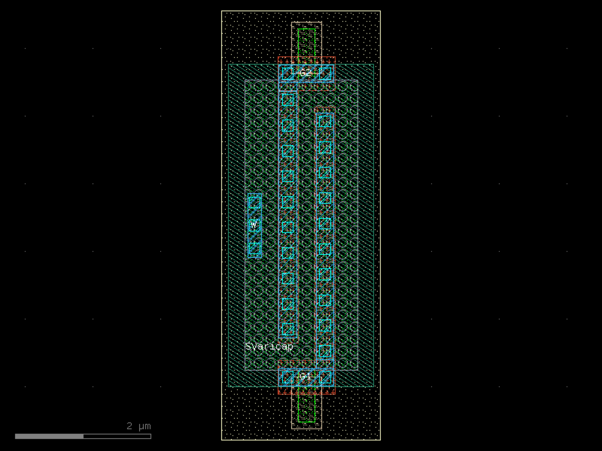
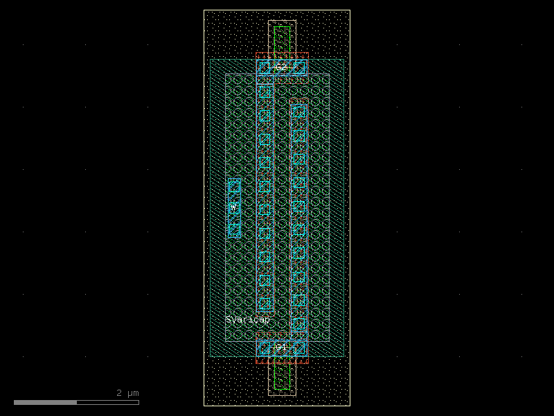
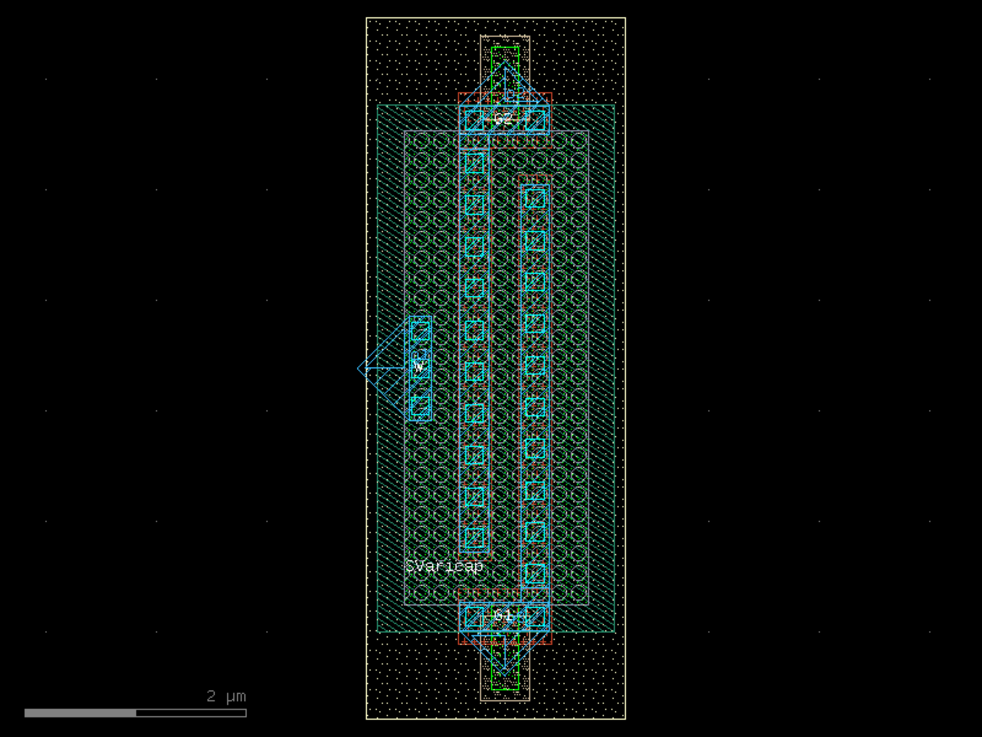
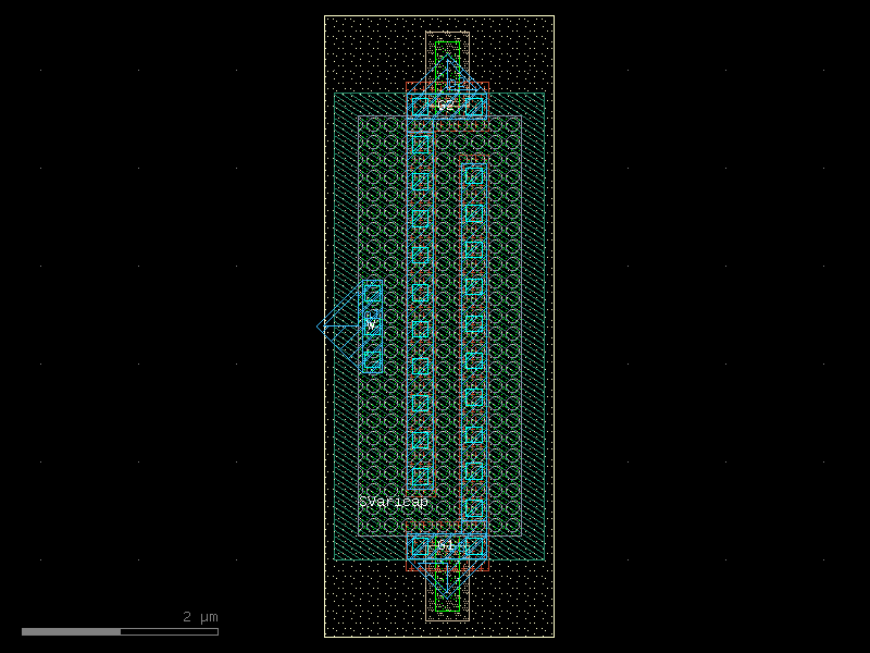
svaricap#
- ihp.cells.svaricap(width=1.0, length=1.0, nf=1, model='sg13_hv_svaricap', layer_nwell='NWelldrawing', layer_activ='Activdrawing', layer_gatpoly='GatPolydrawing', layer_nsd='nSDdrawing', layer_cont='Contdrawing', layer_metal1='Metal1drawing', layer_metal1_pin='Metal1pin', layer_varicap='Varicapdrawing')[source]#
Create a MOS varicap (variable capacitor).
- Parameters:
width (float) – Width of the varicap in micrometers.
length (float) – Length of the varicap in micrometers.
nf (int) – Number of fingers.
model (str) – Device model name.
layer_nwell (tuple[int, int] | str | int | LayerEnum) – N-well layer.
layer_activ (tuple[int, int] | str | int | LayerEnum) – Active region layer.
layer_gatpoly (tuple[int, int] | str | int | LayerEnum) – Gate polysilicon layer.
layer_nsd (tuple[int, int] | str | int | LayerEnum) – N+ source/drain doping layer.
layer_cont (tuple[int, int] | str | int | LayerEnum) – Contact layer.
layer_metal1 (tuple[int, int] | str | int | LayerEnum) – Metal1 layer.
layer_varicap (tuple[int, int] | str | int | LayerEnum) – Varicap marker layer.
layer_metal1_pin (tuple[int, int] | str | int | LayerEnum)
- Returns:
Component with varicap layout.
- Return type:
Component
import warnings
warnings.filterwarnings("ignore", category=DeprecationWarning)

from ihp import PDK
from ihp import cells

PDK.activate()

c = cells.svaricap(width=1.0, length=1.0, nf=1, model='sg13_hv_svaricap', layer_nwell='NWelldrawing', layer_activ='Activdrawing', layer_gatpoly='GatPolydrawing', layer_nsd='nSDdrawing', layer_cont='Contdrawing', layer_metal1='Metal1drawing', layer_metal1_pin='Metal1pin', layer_varicap='Varicapdrawing').copy()
c.draw_ports()
c.plot()
(Source code, png, hires.png, pdf)

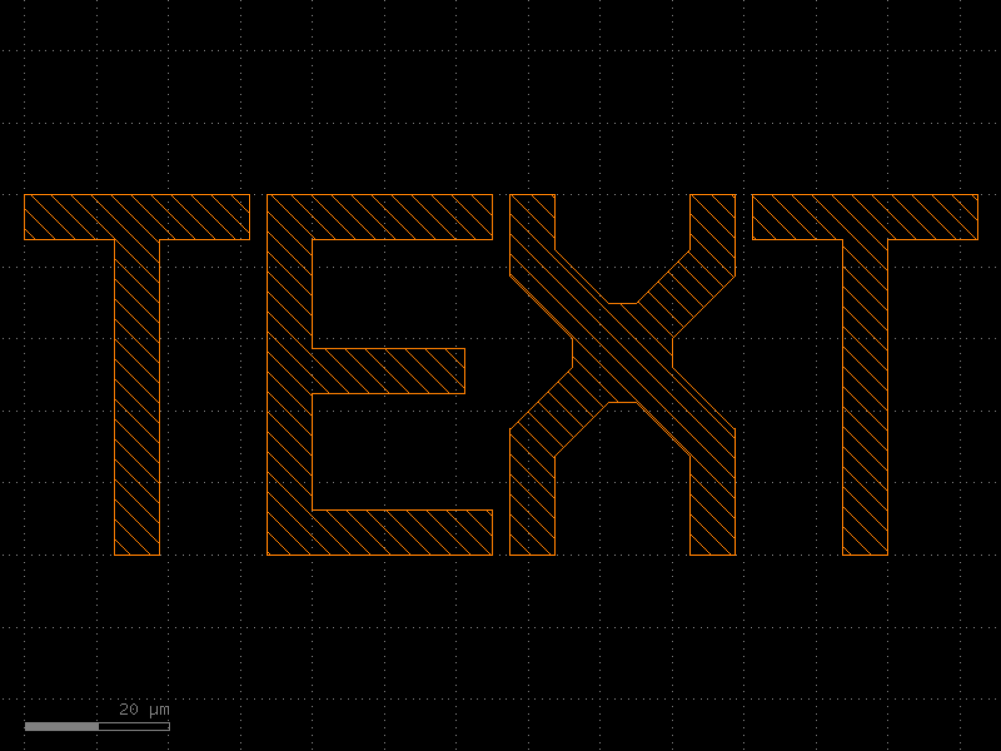
text_rectangular#
- ihp.cells.text_rectangular(text='abc', size=3, justify='left', layer='TopMetal2drawing')[source]#
Pixel based font, guaranteed to be manhattan, without acute angles.
- Parameters:
text (str) – string.
size (float) – pixel size.
justify (str) – left, right or center.
layer (tuple[int, int] | str | int | LayerEnum) – for text.
- Return type:
Component
import warnings
warnings.filterwarnings("ignore", category=DeprecationWarning)

from ihp import PDK
from ihp import cells

PDK.activate()

c = cells.text_rectangular(text='abc', size=3, justify='left', layer='TopMetal2drawing').copy()
c.draw_ports()
c.plot()
(Source code, png, hires.png, pdf)

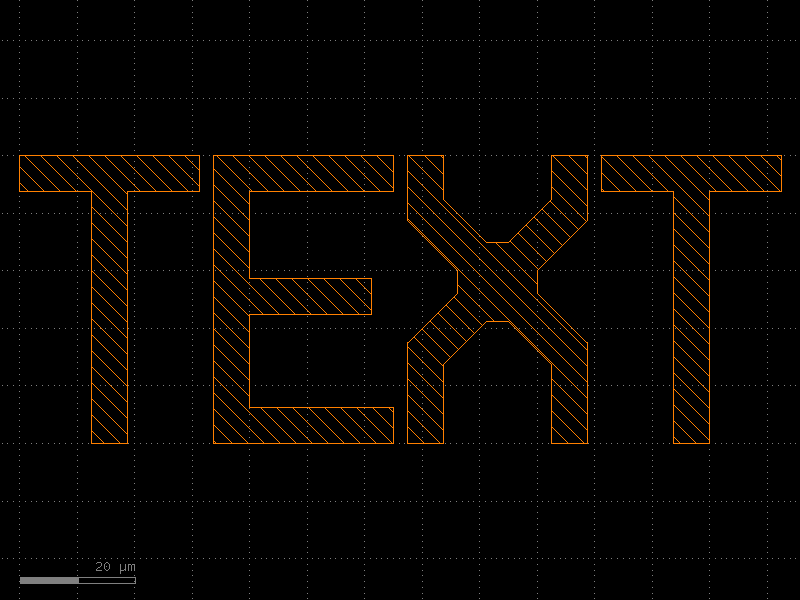
text_rectangular_multi_layer#
- ihp.cells.text_rectangular_multi_layer(text='abc', layers=('TopMetal2drawing',), text_factory='text_rectangular', **kwargs)[source]#
Returns rectangular text in different layers.
- Parameters:
text (str) – string of text.
layers (Sequence[tuple[int, int] | str | int | LayerEnum]) – list of layers to replicate the text.
text_factory (str | Callable[[...], Component] | dict[str, Any] | DKCell | partial[Component]) – function to create the text Components.
kwargs (Any) – keyword arguments for text_factory.
- Return type:
Component
import warnings
warnings.filterwarnings("ignore", category=DeprecationWarning)

from ihp import PDK
from ihp import cells

PDK.activate()

c = cells.text_rectangular_multi_layer(text='abc', layers=('TopMetal2drawing',), text_factory='text_rectangular').copy()
c.draw_ports()
c.plot()
(Source code, png, hires.png, pdf)
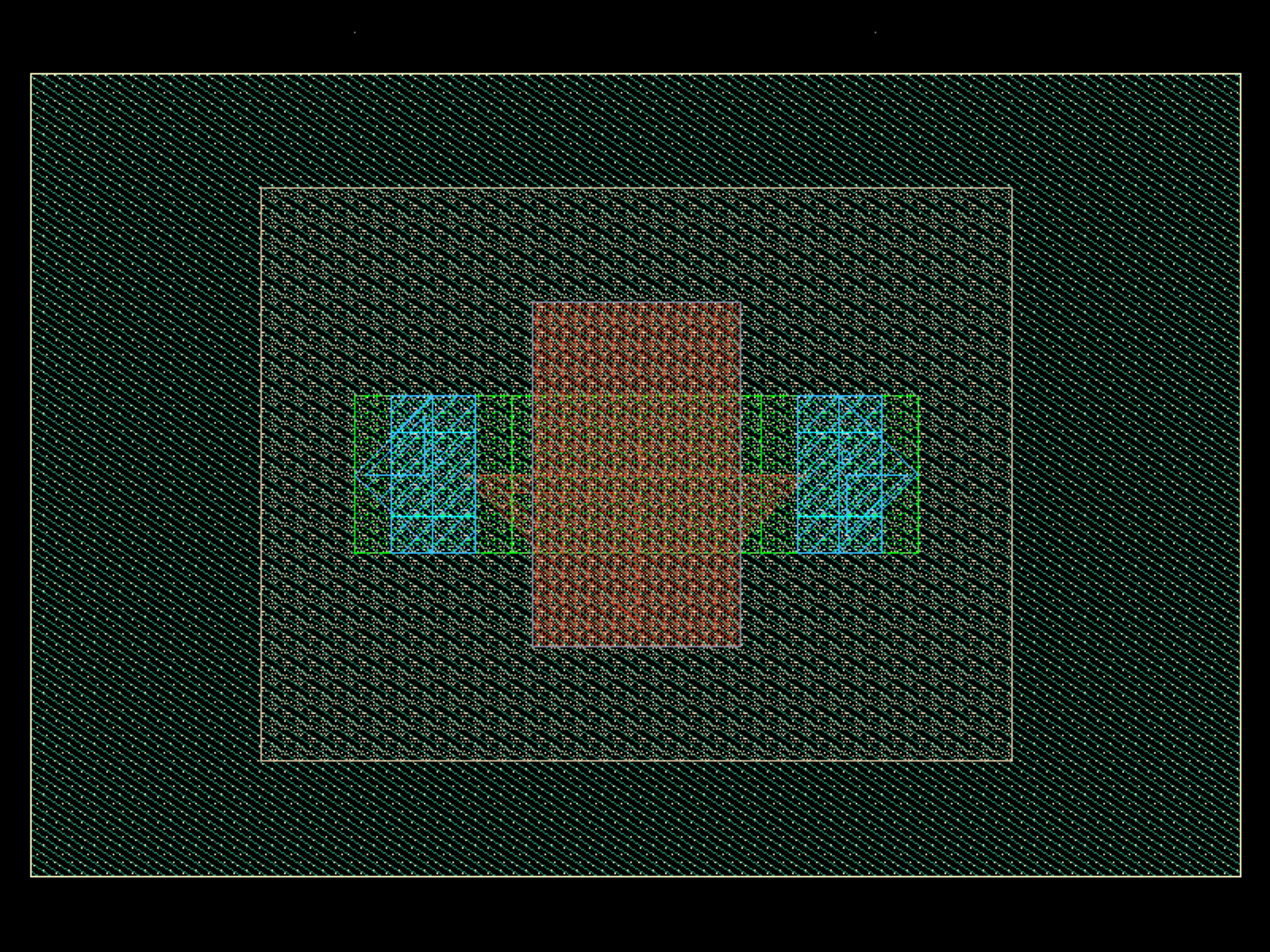
via_array#
- ihp.cells.via_array(via_type='Via1', columns=2, rows=2, via_size=None, via_spacing=None, via_enclosure=None, layer_cont='Contdrawing', layer_via1='Via1drawing', layer_via2='Via2drawing', layer_via3='Via3drawing', layer_via4='Via4drawing', layer_vmim='Vmimdrawing', layer_topvia1='TopVia1drawing', layer_topvia2='TopVia2drawing')[source]#
Create an array of vias.
- Parameters:
via_type (str) – Type of via (Via1, Via2, Via3, Via4, TopVia1, TopVia2).
columns (int) – Number of via columns.
rows (int) – Number of via rows.
via_size (float | None) – Via size in micrometers (uses default if None).
via_spacing (float | None) – Via spacing in micrometers (uses default if None).
via_enclosure (float | None) – Metal enclosure in micrometers (uses default if None).
layer_via1 (tuple[int, int] | str | int | LayerEnum) – Via1 layer.
layer_via2 (tuple[int, int] | str | int | LayerEnum) – Via2 layer.
layer_via3 (tuple[int, int] | str | int | LayerEnum) – Via3 layer.
layer_via4 (tuple[int, int] | str | int | LayerEnum) – Via4 layer.
layer_topvia1 (tuple[int, int] | str | int | LayerEnum) – TopVia1 layer.
layer_topvia2 (tuple[int, int] | str | int | LayerEnum) – TopVia2 layer.
layer_cont (tuple[int, int] | str | int | LayerEnum)
layer_vmim (tuple[int, int] | str | int | LayerEnum)
- Returns:
Component with via array.
- Return type:
Component
import warnings
warnings.filterwarnings("ignore", category=DeprecationWarning)

from ihp import PDK
from ihp import cells

PDK.activate()

c = cells.via_array(via_type='Via1', columns=2, rows=2, layer_cont='Contdrawing', layer_via1='Via1drawing', layer_via2='Via2drawing', layer_via3='Via3drawing', layer_via4='Via4drawing', layer_vmim='Vmimdrawing', layer_topvia1='TopVia1drawing', layer_topvia2='TopVia2drawing').copy()
c.draw_ports()
c.plot()
(Source code, png, hires.png, pdf)

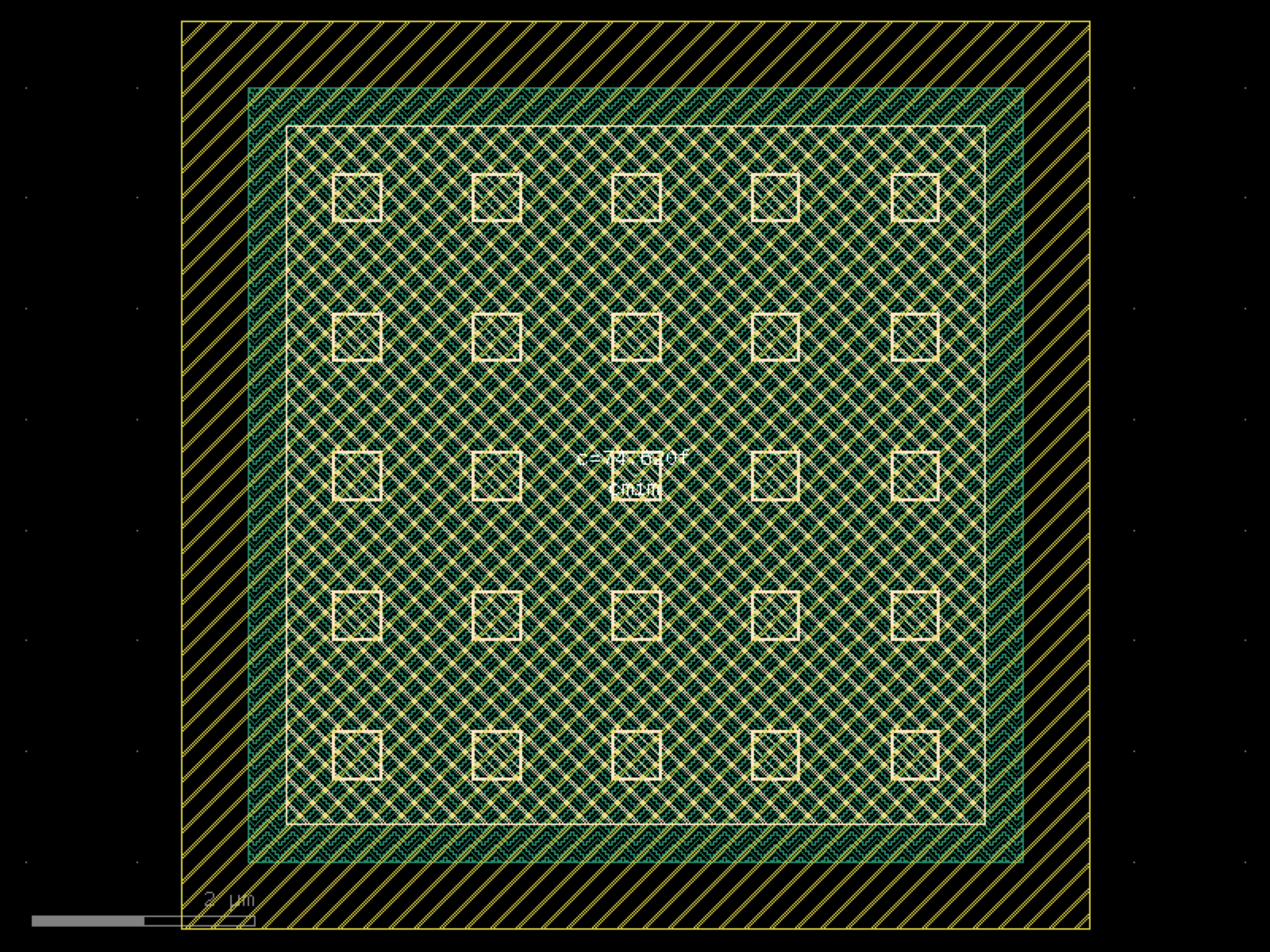
via_stack#
- ihp.cells.via_stack(bottom_layer='Metal1', top_layer='Metal2', size=(10.0, 10.0), vn_columns=2, vn_rows=2, vt1_columns=1, vt1_rows=1, vt2_columns=1, vt2_rows=1, layer_activ='Activdrawing', layer_gatpoly='GatPolydrawing', layer_metal1='Metal1drawing', layer_metal2='Metal2drawing', layer_metal3='Metal3drawing', layer_metal4='Metal4drawing', layer_metal5='Metal5drawing', layer_topmetal1='TopMetal1drawing', layer_topmetal2='TopMetal2drawing', layer_activ_pin='Activpin', layer_gatpoly_pin='GatPolypin', layer_metal1_pin='Metal1pin', layer_metal2_pin='Metal2pin', layer_metal3_pin='Metal3pin', layer_metal4_pin='Metal4pin', layer_metal5_pin='Metal5pin', layer_topmetal1_pin='TopMetal1pin', layer_topmetal2_pin='TopMetal2pin', layer_cont='Contdrawing', layer_via1='Via1drawing', layer_via2='Via2drawing', layer_via3='Via3drawing', layer_via4='Via4drawing', layer_topvia1='TopVia1drawing', layer_topvia2='TopVia2drawing')[source]#
Create a via stack connecting multiple metal layers.
bottom_layer can be Activ, GatPoly, or any metal (Metal1-TopMetal2). Activ and GatPoly connect to Metal1 through Cont; they are independent paths and must not appear together in the same stack.
- Parameters:
bottom_layer (str) – Bottom layer name (Activ, GatPoly, or Metal1-TopMetal2).
top_layer (str) – Top metal layer name (Metal1-TopMetal2).
size (tuple[float, float]) – Size of the metal stack (width, height) in micrometers.
vn_columns (int) – Number of columns for normal vias (Cont, Via1-Via4).
vn_rows (int) – Number of rows for normal vias.
vt1_columns (int) – Number of columns for TopVia1.
vt1_rows (int) – Number of rows for TopVia1.
vt2_columns (int) – Number of columns for TopVia2.
vt2_rows (int) – Number of rows for TopVia2.
layer_activ (tuple[int, int] | str | int | LayerEnum)
layer_gatpoly (tuple[int, int] | str | int | LayerEnum)
layer_metal1 (tuple[int, int] | str | int | LayerEnum)
layer_metal2 (tuple[int, int] | str | int | LayerEnum)
layer_metal3 (tuple[int, int] | str | int | LayerEnum)
layer_metal4 (tuple[int, int] | str | int | LayerEnum)
layer_metal5 (tuple[int, int] | str | int | LayerEnum)
layer_topmetal1 (tuple[int, int] | str | int | LayerEnum)
layer_topmetal2 (tuple[int, int] | str | int | LayerEnum)
layer_activ_pin (tuple[int, int] | str | int | LayerEnum)
layer_gatpoly_pin (tuple[int, int] | str | int | LayerEnum)
layer_metal1_pin (tuple[int, int] | str | int | LayerEnum)
layer_metal2_pin (tuple[int, int] | str | int | LayerEnum)
layer_metal3_pin (tuple[int, int] | str | int | LayerEnum)
layer_metal4_pin (tuple[int, int] | str | int | LayerEnum)
layer_metal5_pin (tuple[int, int] | str | int | LayerEnum)
layer_topmetal1_pin (tuple[int, int] | str | int | LayerEnum)
layer_topmetal2_pin (tuple[int, int] | str | int | LayerEnum)
layer_cont (tuple[int, int] | str | int | LayerEnum)
layer_via1 (tuple[int, int] | str | int | LayerEnum)
layer_via2 (tuple[int, int] | str | int | LayerEnum)
layer_via3 (tuple[int, int] | str | int | LayerEnum)
layer_via4 (tuple[int, int] | str | int | LayerEnum)
layer_topvia1 (tuple[int, int] | str | int | LayerEnum)
layer_topvia2 (tuple[int, int] | str | int | LayerEnum)
- Returns:
Component with via stack.
- Return type:
Component
import warnings
warnings.filterwarnings("ignore", category=DeprecationWarning)

from ihp import PDK
from ihp import cells

PDK.activate()

c = cells.via_stack(bottom_layer='Metal1', top_layer='Metal2', size=(10.0, 10.0), vn_columns=2, vn_rows=2, vt1_columns=1, vt1_rows=1, vt2_columns=1, vt2_rows=1, layer_activ='Activdrawing', layer_gatpoly='GatPolydrawing', layer_metal1='Metal1drawing', layer_metal2='Metal2drawing', layer_metal3='Metal3drawing', layer_metal4='Metal4drawing', layer_metal5='Metal5drawing', layer_topmetal1='TopMetal1drawing', layer_topmetal2='TopMetal2drawing', layer_activ_pin='Activpin', layer_gatpoly_pin='GatPolypin', layer_metal1_pin='Metal1pin', layer_metal2_pin='Metal2pin', layer_metal3_pin='Metal3pin', layer_metal4_pin='Metal4pin', layer_metal5_pin='Metal5pin', layer_topmetal1_pin='TopMetal1pin', layer_topmetal2_pin='TopMetal2pin', layer_cont='Contdrawing', layer_via1='Via1drawing', layer_via2='Via2drawing', layer_via3='Via3drawing', layer_via4='Via4drawing', layer_topvia1='TopVia1drawing', layer_topvia2='TopVia2drawing').copy()
c.draw_ports()
c.plot()
(Source code, png, hires.png, pdf)
via_stack_with_pads#
- ihp.cells.via_stack_with_pads(bottom_layer='Metal1', top_layer='TopMetal2', size=(10.0, 10.0), pad_size=(20.0, 20.0), pad_spacing=50.0, layer_activ='Activdrawing', layer_gatpoly='GatPolydrawing', layer_metal1='Metal1drawing', layer_metal2='Metal2drawing', layer_metal3='Metal3drawing', layer_metal4='Metal4drawing', layer_metal5='Metal5drawing', layer_topmetal1='TopMetal1drawing', layer_topmetal2='TopMetal2drawing', layer_activ_pin='Activpin', layer_gatpoly_pin='GatPolypin', layer_metal1_pin='Metal1pin', layer_metal2_pin='Metal2pin', layer_metal3_pin='Metal3pin', layer_metal4_pin='Metal4pin', layer_metal5_pin='Metal5pin', layer_topmetal1_pin='TopMetal1pin', layer_topmetal2_pin='TopMetal2pin', layer_cont='Contdrawing', layer_via1='Via1drawing', layer_via2='Via2drawing', layer_via3='Via3drawing', layer_via4='Via4drawing', layer_topvia1='TopVia1drawing', layer_topvia2='TopVia2drawing')[source]#
Create a via stack with test pads.
- Parameters:
bottom_layer (str) – Bottom layer name (Activ, GatPoly, or Metal1-TopMetal2).
top_layer (str) – Top metal layer name (Metal1-TopMetal2).
size (tuple[float, float]) – Size of the via stack (width, height) in micrometers.
pad_size (tuple[float, float]) – Size of the test pads (width, height) in micrometers.
pad_spacing (float) – Spacing between pads in micrometers.
layer_activ (tuple[int, int] | str | int | LayerEnum)
layer_gatpoly (tuple[int, int] | str | int | LayerEnum)
layer_metal1 (tuple[int, int] | str | int | LayerEnum)
layer_metal2 (tuple[int, int] | str | int | LayerEnum)
layer_metal3 (tuple[int, int] | str | int | LayerEnum)
layer_metal4 (tuple[int, int] | str | int | LayerEnum)
layer_metal5 (tuple[int, int] | str | int | LayerEnum)
layer_topmetal1 (tuple[int, int] | str | int | LayerEnum)
layer_topmetal2 (tuple[int, int] | str | int | LayerEnum)
layer_activ_pin (tuple[int, int] | str | int | LayerEnum)
layer_gatpoly_pin (tuple[int, int] | str | int | LayerEnum)
layer_metal1_pin (tuple[int, int] | str | int | LayerEnum)
layer_metal2_pin (tuple[int, int] | str | int | LayerEnum)
layer_metal3_pin (tuple[int, int] | str | int | LayerEnum)
layer_metal4_pin (tuple[int, int] | str | int | LayerEnum)
layer_metal5_pin (tuple[int, int] | str | int | LayerEnum)
layer_topmetal1_pin (tuple[int, int] | str | int | LayerEnum)
layer_topmetal2_pin (tuple[int, int] | str | int | LayerEnum)
layer_cont (tuple[int, int] | str | int | LayerEnum)
layer_via1 (tuple[int, int] | str | int | LayerEnum)
layer_via2 (tuple[int, int] | str | int | LayerEnum)
layer_via3 (tuple[int, int] | str | int | LayerEnum)
layer_via4 (tuple[int, int] | str | int | LayerEnum)
layer_topvia1 (tuple[int, int] | str | int | LayerEnum)
layer_topvia2 (tuple[int, int] | str | int | LayerEnum)
- Returns:
Component with via stack and test pads.
- Return type:
Component
import warnings
warnings.filterwarnings("ignore", category=DeprecationWarning)

from ihp import PDK
from ihp import cells

PDK.activate()

c = cells.via_stack_with_pads(bottom_layer='Metal1', top_layer='TopMetal2', size=(10.0, 10.0), pad_size=(20.0, 20.0), pad_spacing=50.0, layer_activ='Activdrawing', layer_gatpoly='GatPolydrawing', layer_metal1='Metal1drawing', layer_metal2='Metal2drawing', layer_metal3='Metal3drawing', layer_metal4='Metal4drawing', layer_metal5='Metal5drawing', layer_topmetal1='TopMetal1drawing', layer_topmetal2='TopMetal2drawing', layer_activ_pin='Activpin', layer_gatpoly_pin='GatPolypin', layer_metal1_pin='Metal1pin', layer_metal2_pin='Metal2pin', layer_metal3_pin='Metal3pin', layer_metal4_pin='Metal4pin', layer_metal5_pin='Metal5pin', layer_topmetal1_pin='TopMetal1pin', layer_topmetal2_pin='TopMetal2pin', layer_cont='Contdrawing', layer_via1='Via1drawing', layer_via2='Via2drawing', layer_via3='Via3drawing', layer_via4='Via4drawing', layer_topvia1='TopVia1drawing', layer_topvia2='TopVia2drawing').copy()
c.draw_ports()
c.plot()
(Source code, png, hires.png, pdf)
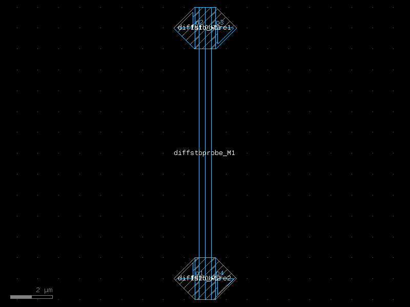
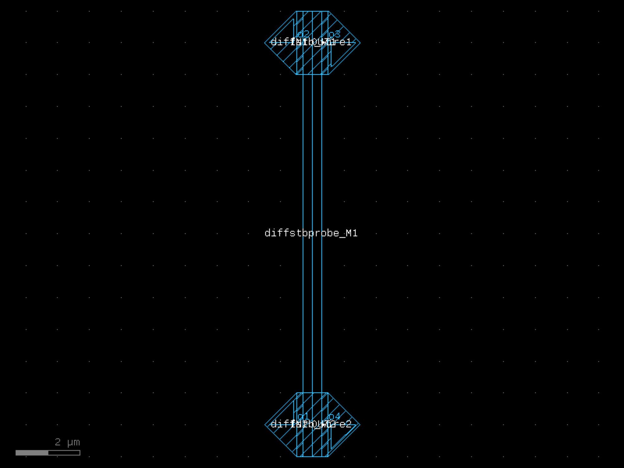

wire_corner#
- ihp.cells.wire_corner(cross_section='metal_routing', width=None)[source]#
Returns 45 degrees electrical corner wire.
- Parameters:
cross_section (CrossSection | str | dict[str, Any] | Callable[[...], CrossSection] | SymmetricalCrossSection | DCrossSection) – spec.
width (float | None) – optional width. Defaults to cross_section width.
- Return type:
Component
import warnings
warnings.filterwarnings("ignore", category=DeprecationWarning)

from ihp import PDK
from ihp import cells

PDK.activate()

c = cells.wire_corner(cross_section='metal_routing').copy()
c.draw_ports()
c.plot()
(Source code, png, hires.png, pdf)
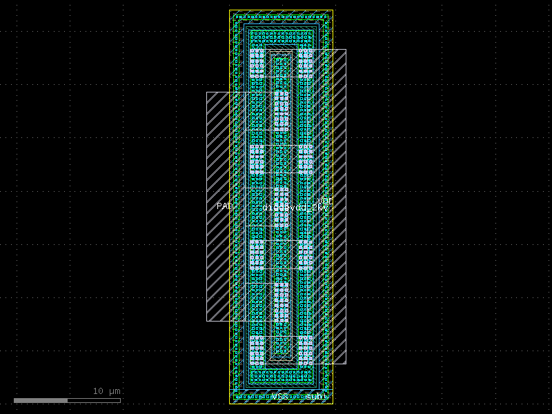
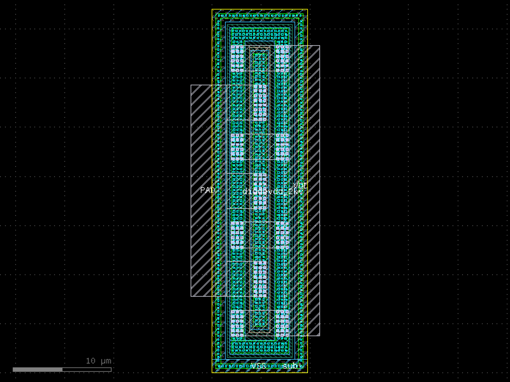

wire_corner45#
- ihp.cells.wire_corner45(cross_section='metal_routing', radius=10, width=None, layer=None, with_corner90_ports=True)[source]#
Returns 90 degrees electrical corner wire.
- Parameters:
cross_section (CrossSection | str | dict[str, Any] | Callable[[...], CrossSection] | SymmetricalCrossSection | DCrossSection) – spec.
radius (float) – ignored.
width (float | None) – optional width. Defaults to cross_section width.
layer (tuple[int, int] | str | int | LayerEnum | None) – ignored.
with_corner90_ports (bool) – if True, adds ports at 90 degrees.
- Return type:
Component
import warnings
warnings.filterwarnings("ignore", category=DeprecationWarning)

from ihp import PDK
from ihp import cells

PDK.activate()

c = cells.wire_corner45(cross_section='metal_routing', radius=10, with_corner90_ports=True).copy()
c.draw_ports()
c.plot()
(Source code, png, hires.png, pdf)
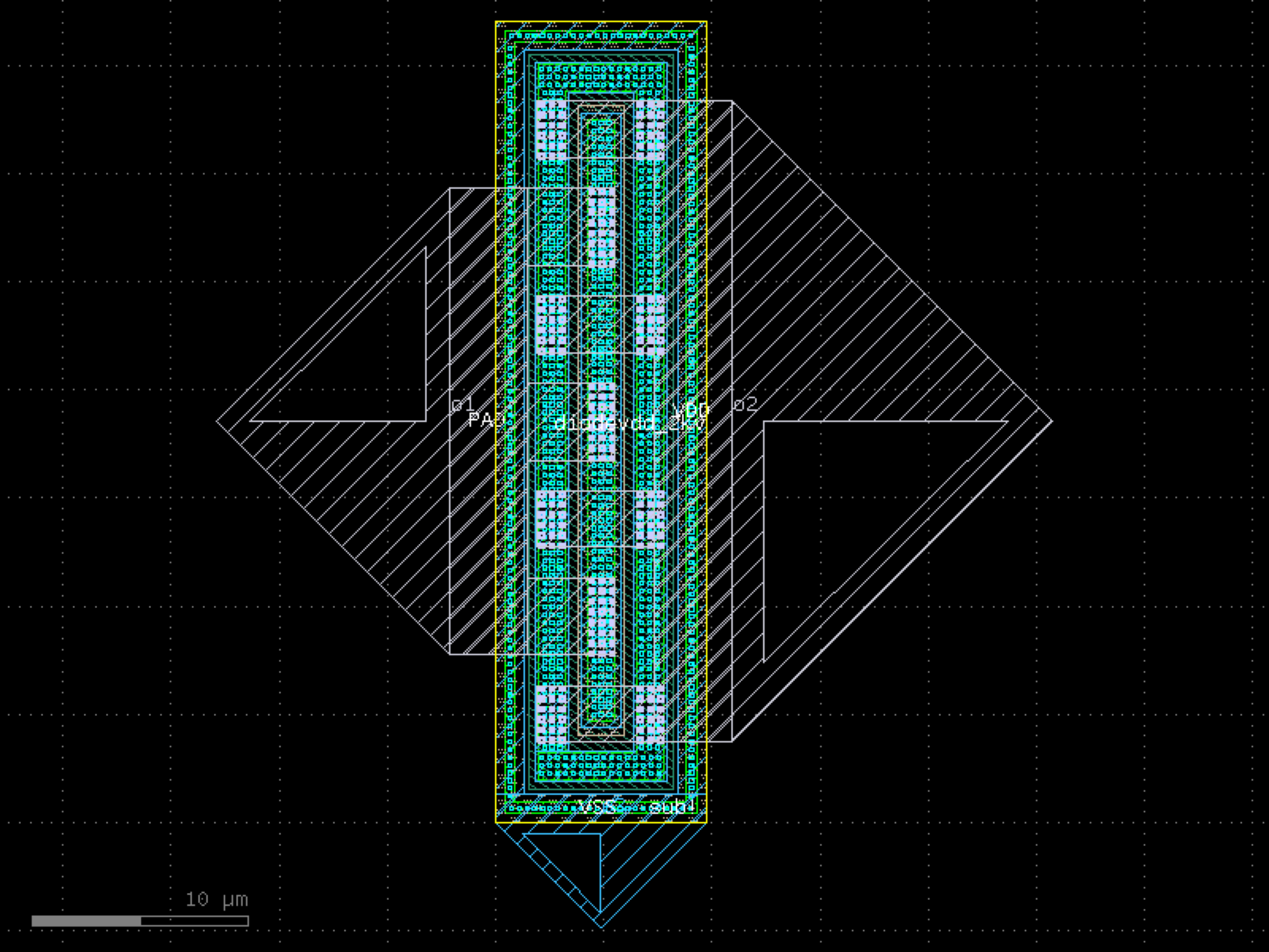