Abstract
Designing an EPIC -- and (electronic) photonic integrated circuit -- requires robust tooling ranging from exploratory simulation via mask layout and verification to validation. In the past a variety of specialized syntaxes were introduced with similar tooling for electronic chip design -- the older cousin of EPICs. The relatively young age of integrated photonics opens up the opportunity to establish an accessible workflow which is intuitive, easily customizeable and extensible. GDSFactory is a python based framework to build EPICs that provides a common syntax for design/layout, simulation (Ansys Lumerical, tidy3d, MEEP, MPB, DEVSIM, SAX, Elmer, Palace, …), verification (Klayout DRC, LVS, netlist extraction, connectivity checks, fabrication models) and validation. This paper showcases the capabilities of GDSFactory, highlighting its end-to-end workflow, which enables users to turn their chip designs into working products.
Introduction
Hardware iterations typically require months of time and involve substantial financial investments, often in the millions of dollars. In contrast, software iterations can be completed within hours and at a significantly lower cost, typically in the hundreds of dollars. Recognizing this discrepancy, GDSFactory aims to bridge the gap by leveraging the advantages of software workflows in the context of hardware chip development.
To achieve this, GDSFactory offers a comprehensive solution through a unified python API. This API enables users to drive various aspects of the chip development process, including layout design, verification (such as optimization, simulation, and design rule checking), and validation (through the implementation of test protocols). By consolidating these functionalities into a single interface, GDSFactory streamlines the workflow and enhances the efficiency of hardware chip development.
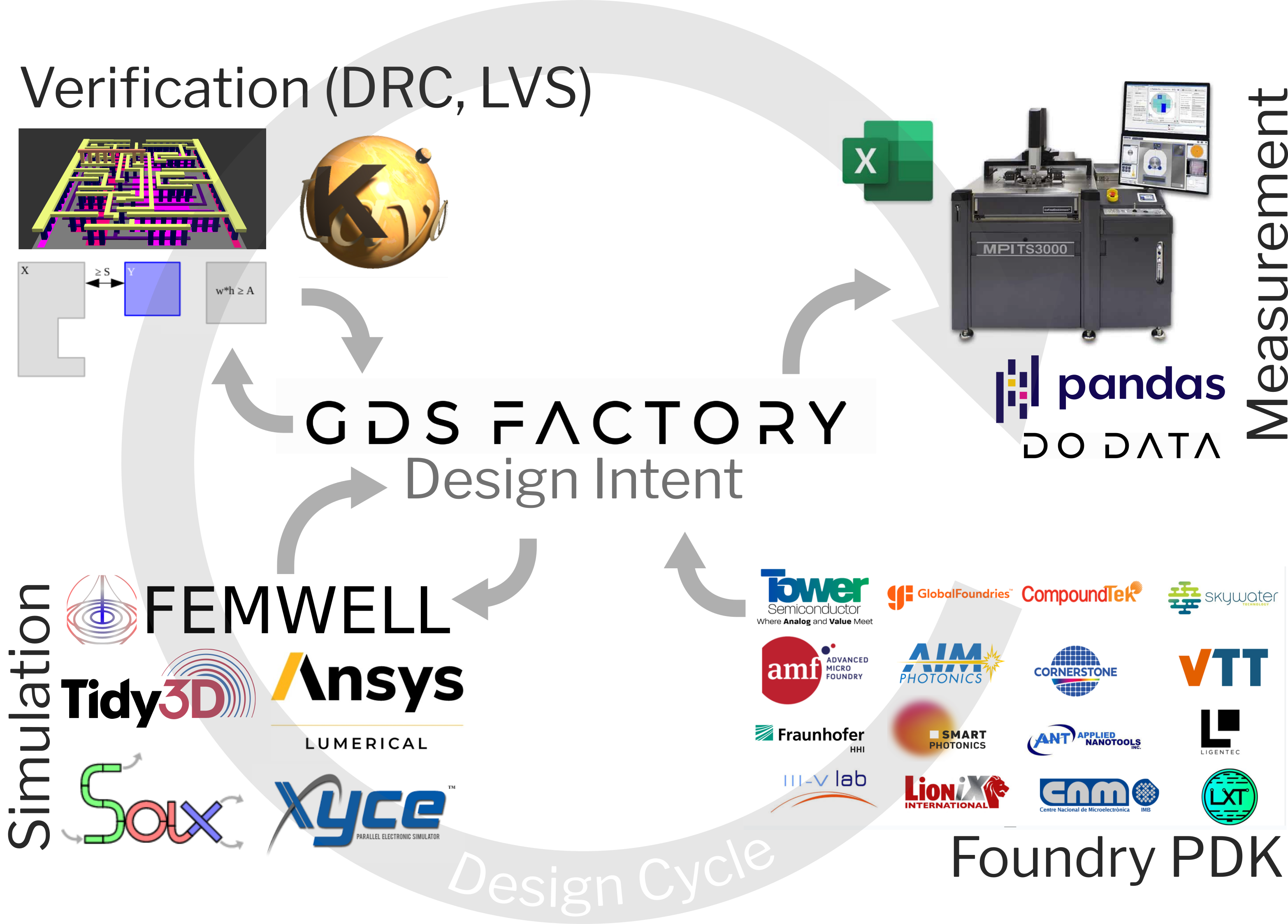
GDSFactory bridges the whole EPIC design cycle, with a variety of Foundary PDKs available it is both easy to construct circuits reusing proven devices and to realize conceptually new designs. The generated component layouts can be used in varous simulators for exploration, optimization and validation. GDSfactory tightly integrates with KLayout, leveraging its advanced design rule checks (DRC) and layout versus schematic (LVS) capabilities. For characterization of the fabricated devices GDSFactory provides rich metadata compatible to commercial wafer probers, including the position and orientation of fiber-to-waveguide couplers.
GDSFactory acts a as a unifying framework covering the entire EPIC design cycle. It allows the user to:
Design (Layout, Simulation, Optimization)
Capture design intent in a schematic and automatically generate a layout.
Define parametric cells (PCells) functions in
pythonorYAML. Define routes between component ports.Test component settings, ports and geometry to avoid unwanted regressions.
Verify (DRC, DFM, LVS)
Run simulations directly from the layout thanks to the simulation interfaces. No need to draw the geometry more than once.
Run Component simulations (EM solver, FDTD, EME, TCAD, thermal …)
Run Circuit simulations from the Component netlist (Sparameters, Spice)
Build Component models and study Design For Manufacturing.
Create DRC rule decks.
Make sure complex layouts match their design intent (Layout Versus Schematic).
Measure and Validate
Make sure that as you define the layout you define the test sequence, so when the chips come back you already know how to test them.
Model extraction: extract the important parameters for each component.
Build a data pipeline from raw data, to structured data and dashboards for monitoring your chip performance.
In this paper we will highlight the key features of GDSFactory follwing the structure of the design cycle shown in Figure 1. To contextualize the demonstrated features we will in parallel develop a simple photonic transceiver circuit as a case study. This will allow us to paint a more cohesive picture showcasing GDSFactory’s particular strengths.
Design Flow
GDSFactory offers a range of design capabilities, including layout description, optimization, and simulation. It allows users to define parametric cells (PCells) in python, facilitating the creation of complex components. The library supports the simulation of components using different solvers, such as mode solvers (finite element and finite difference eigenmode solvers), eigenmode expansion methods (EME), TCAD and thermal simulators, and fullwave FDTD simulations. Optimization capabilities are also available through an integration with Ray Tune, and automatically differentiable solvers enabling efficient parameter tuning for improved performance.
In the following we design a comparatively simple photonic transceiver based on modulators, that leverage electro optic polymers edposited inside slit waveguides and germanium photodetectors for detection. Later, coarse wavelength division multiplexing will be performed using coupled ring oscillator waveguides as routers/bandfilters. These examples concentrate on photonic integrated design, however they are readily adaptable for RF and analog circuit design.
Mask Layout
Generating mask layouts ready for fabrication is the core functionality of GDSFactory. As input, GDSFactory supports 3 different workflows that can be also mixed and matched.
Write
pythoncode. Recommended for developing cell libraries.Write
YAMLcode to describe your circuit. Recommended for circuit design. Notice that theYAMLincludes schematic information (instances and routes) as well as Layout information (placements).Define schematic, export SPICE netlist, convert SPICE to
YAMLand tweakYAML.
As output you write a GDSII or OASIS file that you can send to your foundry for fabrication. It also exports component settings (for measurement and data analysis) and netlists (for circuit simulations).
We will start our design by constructing a strip-to-slot converter, which interfaces strip waveguides used to route light across the chip to the slot waveguides of the modulators. These simple passive component will allow us to clearly demonstrate the more fundamental step of mask-design, like polygon manipulation, waveguide cross sections and ports. In the course of this section we will work our way to higher levels of abstraction, which help handling the complexity of large scale designs.
import gdsfactory as gf
from gdsfactory.gpdk import PDK
PDK.activate()

# Create a blank component
# (essentially an empty GDS cell
# with some special features).
c = gf.Component()

w_I, w_II, g, L = 0.4, 0.66, 0.1, 3.0

# Add some geometry to it.
polygon_taper = c.add_polygon(
    [(0, 0), (L, 0),
     (L, (w_II-g)/2), (0, w_I)],
    layer=PDK.layers.WG
)

c # Plot it in jupyter notebook.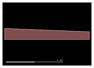
Figure 2:Minimal example demonstrating the most basic functionality of GDSFactory: creating a polygon on a specified layer. (a) Shows the code snippet in python including descriptive comments to highlight selected aspects. All code snippets used throughout this paper can be run interactively in the online version of this paper. (b) The resulting GDSII layout as it would appear in the inline Jupyter notebook viewer shipped with gdsfactory.
Figure 2 shows a minimal example how to create a polygon from a list of points on a specified layer. The snippets also demonstrate some of the steps required to get going:
As with any
pythonlibrary, the first step is to importgdsfactory. For convenience we will alias it asgf.Before we can start designing, we need to activate a process development kit (PDK) that defines the layers and design rules for a specific fabrication process. Here, we use the generic PDK included with GDSFactory. We will discuss Process Development Kits (PDKs) in more details below.
Next we create a blank
Componentinstance that will hold our geometry. It can be understood as an empty GDS cell, that is enriched with additional functionality like metadata and ports.Finally we add the desired polygon to the component by specifying the list of points and the GDS layer we want to add it to.
Lastly we visualize the created geometry using the built-in plotting functionality. In this case we use the inline viewer for Jupyter notebooks. However, GDSFactory also supports synchronization with KLayout for advanced visualization and verification. Leveraging the export capabilities of GDSFactory, the created layout can be saved and viewed as a GDSII or OASIS file ready for fabrication. (TODO correctly name available formats)
Defining more complex geometries from scratch can quickly become cumbersome. To alleviate this burden GDSFactory provides a rich library of predefined components ranging from geometrical primitives, over labels, structures for process controll like resolution tests and interlayer alignment calipers to common photonic building blocks like waveguides, bends, couplers, interferometers, ring resonators and more. These predefined parametric components can be easily reused in user-defined designs. In Figure 3 we demonstrate such reuse for the case of a waveguide taper, which in combination with the previously defined polygon forms strip-to-slot converter. The snippet follows three main steps:
The component factory[1]
gf.components.tapergenerates a taper componenttwith specific dimensions (i.e. lenght and widths at both ends).A reference to that component is then added to the component
c(from Figure 2):t_ref = c << t. Here,t_refis the reference that was added.Lastly, the reference is moved up to form a consistent gap of size
g. The parent component can in principle contain multiple references to the same underlying geometry, which can be manipulated individually (not shown in the current example). In this way, the resulting GDSII file is significantly lighter, because the geometry is only saved once.
offset = 0.75*w_II + 0.25*g
# Add a predefined symmetric taper
t = gf.components.taper(
    length=L,
    width1=(offset-g-w_I)*2,
    width2=(w_II-g)/2)
t_ref = c << t
t_ref.movey(offset)
c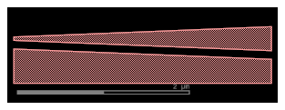
Figure 3:Reusing predefined components (PCells). (a) Code snippet demonstrating how to realize predefined components from the GDSFactory library. Subsequently the created geometry can placed (possibly multiple times) into a parent component. The position and orientation of each reference can be manipulated individually. (b) Resulting layout showing the placed rectangle and two instances of the text label with different positions and orientation.
Functions as Parametric Cells (PCells)
As we have seen in Figure 3 GDSFactory provides a mechanism to handle parametric components, that is components whose concrete geometry depends on a set of parameters. In GDSFactory such PCells are defined as python functions decorated with @gf.cell. These functions take parameters as input and have to return a gf.Component instance containing the generated geometry. As such, the PCell definitions inherit the full power and flexibility of the python ecosystem, including control flow and complex arithmetics.
# The @gf.cell decorator makes this function a PCell,
# adding caching and other features.
@gf.cell
def _strip_to_slot(
      w_I = 0.4, w_II = 0.66, g = 0.1, L = 3.0,
    ) -> gf.Component:

    c = gf.Component()
    c.add_polygon(
        [(0, 0), (L, 0), (L, (w_II-g)/2), (0, w_I)],
        layer = PDK.layers.WG
    )

    offset = 0.75*w_II + 0.25*g
    t = gf.components.taper(length=L,
        width1=(offset-g-w_I)*2, width2=(w_II-g)/2)
    (c << t).movey(offset)

    return c

flip(_strip_to_slot(L=4.0)) # Flip for viz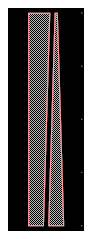
Figure 4:Defining new parametric cells (PCells). (a) Code snippet showing how to define a new parametric cell as a component factory, i.e. a function that returns a gf.Component when called with desired parameters. The particular example is the strip-to-slot converter we had previously contructed in Figure 3 (b) Resulting layout showing the created converter. To enable a compact presentation the converter is flipped by 90° before it’s rendered.
Figure 4 demonstrates how a new PCell can be created. PCells can nest other PCells in order to build arbitrarily complex components. In this case, we are composing one previously defined PCell - the taper - and a custom polygon. The cross section widths, gap size and length are exposed as input parameter. Based on this ability to compose PCells, GDSFactory enables large scale hierarchical layouts, where the composition of simpler building blocks allows the designer to reduce complexity by hiding implementation details behind layers of abstraction.
(Automatic) Routing
Integrated photonics relies at its core on waveguides to route light between different devices on chip. In contrast to low-speed electrical interconnects, waveguides require careful matching of the cross-sectional geometry at all interfaces to avoid unwanted reflections and losses. To facilitate connecting different components, GDSFactory leverages directional ports. Each port defines not only its position, but also its orientation and cross-section, enabling reliable mutual alignment when connecting different components.
@gf.cell
def strip_to_slot(
      w_I = 0.4, w_II = 0.66,
      g = 0.1, L = 3.0,
    ) -> gf.Component:

    c = gf.Component()
    c << _strip_to_slot(w_I, w_II, g, L)

    kwargs = dict(layer=PDK.layers.WG, port_type='optical')

    c.add_port(
        name='o1', width=w_I,
        orientation=180, center=(0, w_I/2),
        **kwargs
    )

    c.add_port(
        name='o2', width=w_II, cross_section=xs_slot,
        orientation=0, center=(L, w_II/2),
        **kwargs
    )

    return c

I2II = strip_to_slot().copy()
I2II.draw_ports()
flip(I2II)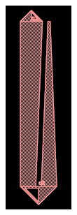
Figure 5:Adding port metadata. (a) Code snippet demonstrating how ports can be added to a PCell and how they can be vizualized using c.draw_ports(). (b) Resulting layout including port indicators (flipped by 90° for compact display).
To allow connecting our strip-to-slot converter to appropriate waveguides later, we add the port information in Figure 5 using the c.add_port function. The @gf.cell decorator caches components which were previously generated with the same input parameters. This makes sure that we add multiple references to the same component instead of replicating the component to reduce the GDSII file size and the associated computational burden. This however, leads to a small complication when adding port indicators using c.draw_ports(), because the indicators are directly written into the components geometry. To avoid poluting the cache with invalid geometry, we .copy() the component and only insert the port markers into the copy.
Further, c.pprint_ports() prints the port properties in a human-readable format (see Figure 6).
I2II.pprint_ports()Figure 6:Retreiving port information in a human readable form (a) Code snippet reusing the component I2II previously defined in Figure 5 (b) A table containing the port names, positions, orientations and cross-sections of the component. To appreciate the port center (x, y) coordinates, consider that the rendered geometry in Figure 5 is flipped by 90°.
NOTE: From here on things are still veeeeerrry rough TODO: Explain aligning Components by their ports.
@gf.cell
def convert_and_bend() -> gf.Component:
  c = gf.Component()
  I2II = c << strip_to_slot(L=4.0)

  bend = c << (
      gf.components.bend_euler(
        radius=5,
        width=I2II.ports["o1"].width)
  )
  bend.connect("o1", I2II.ports["o1"])

  c.add_port("o1", port=bend.ports["o2"])
  c.add_port("o2", port=I2II.ports["o2"])

  return c

c_convert_and_bend = convert_and_bend()
c_convert_and_bend.draw_ports()
flip(c_convert_and_bend)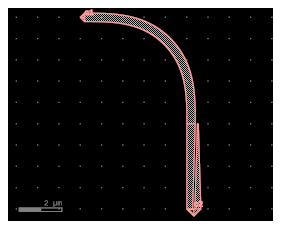
Figure 7:Aligning components by connecting their ports.
Manually routing complex circuits quickly becomes cumbersome. To alleviate this burden GDSFactory provides a routing API for (semi-)automatic waveguide routing. Given a declarative description of the desired connections it can create single and bundled waveguide routes, that avoid obstacles and collisions between the bundled waveguides. A minimal demonstration of automatically routing a single connection is shown in .
c = gf.Component()
I2II = strip_to_slot()
c << I2II
dummy = gf.components.straight(3)
dummy_ref = c << dummy
dummy_ref.move((40, -20))

# Automatically route a single waveguide
route = gf.routing.route_single(
    c,
    port1=dummy_ref.ports["o1"],
    port2=I2II.ports["o2"],
    cross_section=gf.cross_section.strip,
)
c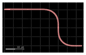
Figure 8:Automatic manhattan routing for a single waveguide connection (a) Code snippet demonstrating how to route a waveguide between two ports (b) Resulting layout showing the automatically create waveguide connection.
Multiple waveguides can be routed simultaneously using bundles. In (#basics-route-multi) we leverage this automatic routing of multiple waveguides to realize a fan-out to four strip to slot converters
c = gf.Component()
converters = [c << I2II for _ in range(4)]
wgs = [c << dummy for _ in range(4)]

for i, conv in enumerate(converters):
    conv.move((13, (i-1.5)*5))

for i, wg in enumerate(wgs):
    wg.movey((i-1.5)*2)

# Automatically route a waveguide
# between the waveguides and converters
gf.routing.route_bundle_sbend(
    c,
    ports1=[wg.ports["o2"] for wg in wgs],
    ports2=[cv.ports["o1"] for cv in converters],
    cross_section=gf.cross_section.strip,
)
flip(c)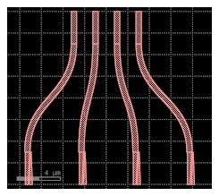
Figure 9:Automatic S-bend routing for a bundle of waveguide connections (a) Code snippet placing and routing input waveguides and fanned out strip-to-slot converters. (b) Resulting layout showing the automatically generated fan out.
YAML based Composition for Large Scale Layouts
While defining PCells in python is very powerful, one commonly simply desires to combine preexisting building block into circuits (as we have already done in and ). In these cases describing the desired circuit in a netlist-like format allows the user to focus on the relevant aspects, while reducing boilerplate. For this purpose GDSFactory establishes a YAML based representation. The specification equivalent to is shown in .
This makes composite designs very scalable, allowing the user to easily design for example parameter variation experiments (DOEs) as shown in Figure 10.
name: mask_compact

instances:
  rings:
    # `pack_doe` is a special function that creates a Design of Experiments array.
    component: pack_doe
    settings:

      # It will create ring resonators with these different radii and coupling lengths.
      doe: ring_single
      max_size : [1500, null]
      settings:
        radius: [20, 30, 40, 50, 60]
        length_x: [1, 2, 3, 4, 5, 6]

      # This tells the function to generate all possible combinations of the specified radius and length_x values.
      do_permutations: True
      function:

        # After each unique ring is created, the add_fiber_array function is applied to it, adding grating couplers for testing.
        function: add_fiber_array
        settings:
            fanout_length: 200

placements:
  rings:
    xmin: 50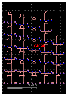
Figure 10:Declaratively describing the desired circuit in YAML format. (a) YAML that is fed to gf.read.from_yaml() to create a circuit layout. The example creates a design of experiments (DoE) array of ring resonators with varying radii and coupling lengths, as well as a grid of Mach-Zehnder Interferometers (MZIs) with different path length differences. Each component is automatically equipped with fiber arrays for testing. (b) Resulting layout showing the created DoE array of ring resonators on the left and the MZI grid on the right.
Continuous Integration: Regression Tests
Demonstrate GDS-diff: Rev 1: fundamental comp -> derived component 1
Rev 2: fundamental comp -> derived component 1 & derived component 2
To introduce derived comp 2 the design engineer introduced changes to fundamental comp -> regression in derived comp 1
-> show GDSdiff.
TODO: Which other Tests to show? Are the regression tests relevant enough to show?
Simulation and Optimization: Layout as Single Source of Truth
The GDSFactory ecosystem supports multiple solvers to simulate the physical behavior of the created design. These cover several aspects, like the optical behavior of single components via finite difference time domain simulations, the collective behavior of multiple coupled components via scattering matrix (S-matrix) circuit simulators, the propagation of thermal transients, electronic properties and more. The single source of truth providing the device geometry, is a key benefit of GDSFactory linking these different simulators together.
Component-Level Simulation
Show extraction of:
S-parameters of strip to slot
S-parameters of coupler TODO: Hey Floris what is the currently preferred way of running fdtd S-matrix extraction simulations? Are open source options available? I think that would make it a lot easier (in contrast to Tidy3D/Lumerical etc.)
Electrical? Would need help for that! There seems to be something going with Palace, but I didn’t really follow the discussion there. Is the EO-polymer example even suitable? Can we do TCAD/electrical simulations for EO-polymer?
Reference to Layer stack (Process Development Kits (PDKs)) Show of 3D view -> probably nicest with some electrical connections/heaters.
Circuit-Level Simulation
Circuit -> CROW with SAX Optimize CROW (I have some material on optimizing the filter poles to match known filter types (e.g. butterworth). But in principle this way of designing filters can even be done analytically. Need to figure out where this would fit in)
Process Development Kits (PDKs)
Few words: what is a PDK
Structure of a PDK in GDSFactory
Layer Definitions
Cross-sections; Layer Stack
Cell-library
Design Rules -> Maybe subsection for each?
Currently Available PDKs
List openly accessible PDKs and PDKs that are available upon request / under NDA. Emphasize portability of high level designs across foundrys. What else would you want to add here?
Verification
TODO: Troy I need help here :/ I do not know much about Verification inf gdsfactory...
Design Rules important part of PDK. Guarantee foundry can fabricate specified structures accurately.
Design Rule Check (DRC)
Uses KLayout for DRC List of design rules supported out of the box
Feature size
Inclusion
Density ...
Layout vs. Schematic (LVS)
What is actually happening here?
Do we check unterminated ports?
As you can see: I have no clue :/
Measurement and Validation
Once design has been sucessfully verified it can be send of to the foundry. Transmitting the design files to the foundry is often referred to as tape-out (historical reference).
Metadata
Demonstrate Fiber Metadata. Wafer prober compatibility. Which wafer probers work? Are there people companies using this? Do we have experimental data we could use to illustrate?
Teststructures
Nonexhaustive List: Available photonic/metrology teststructures (also litho/alignment etc.). Also here: do we have experimental data?
Final: add teststructures to case study mask to complete the tutorial.
TODO: what is missing?
Conclusion
The paper has highlighted the key features and functionalities of GDSFactory for hardware design. By leveraging the power of python, GDSFactory empowers designers with a familiar and flexible programming language widely used in machine learning, scientific computing, and engineering. This enables seamless integration with existing software ecosystems and promotes code reuse and collaboration.
The verification and validation capabilities of GDSFactory play a crucial role in ensuring the manufacturability and functionality of the designed chips. From functional verification to design for robustness and manufacturing, GDSFactory offers tools and methods to design chips, detect potential issues, and optimize performance.
Furthermore, GDSFactory provides an interactive schematic capture feature that enhances the design process and facilitates the alignment between design intent and the produced layout. With support for SPICE and YAML, designers have the flexibility to define and modify schematics in a user-friendly manner, either visually or programmatically.
The ability to define test sequences and measurement parameters within GDSFactory streamlines the post-fabrication testing process. By establishing a clear measurement and data analysis pipeline, designers can evaluate the fabricated components against the design specifications, allowing them to identify and systematically eliminate potential flaws. In conclusion, GDSFactory is a comprehensive and extensible design automation tool that empowers designers to efficiently develop integrated circuits and components. Its python-driven workflow, combined with its integration capabilities, verification tools, schematic capture feature, and test sequence definition, provides a powerful platform for turning chip designs into validated products.
Acknowledgments
We would like to acknowledge all other contributors to the GDSFactory project who at the time of writing are: Simon Bilodeau (Google), Niko Savola (Google, Aalto University), Marc de Cea Falco (Google), Helge Gehring (Google), Yannick Augenstein (FlexCompute), Ryan Camacho (BYU), Sequoia Ploeg (BYU), Prof. Lukas Chrostowski (UBC), Erman Timurdogan (Lumentum), Damien Bonneau (PsiQuantum), Alec Hammond (Meta), Thomas Dorch (HyperLight), Alex Sludds (Lightmatter), Igal Bayn (Quantum Transistors), Skandan Chandrasekar (UWaterloo), Tim Ansell, Ardavan Oskoii (Meta), Bradley Snyder (Superlight) and Amro Tork (Mabrains). Erman Timurdogan contributed the GDSFactory design, verification and validation cycles figure and Dario Quintero contributed the GDSFactory microservices architecture figure.
We would also like to acknowledge the foundational work of other open-source developers: Adam McCaughan (PHIDL), Juan Sanchez (DEVSIM), Matthias Köfferlein (Klayout), Ardavan Oskooi, Alec Hammond, Stephen Johnson (MEEP), Jesse Lu (FDTDZ), Dan Fritchman (VLSIR), Dario Quintero (PIEL), Floris Laporte (SAX, MEOW).
Data Availability
The source code of GDSFactory is available publicly on github under MIT license. The demonstrations presented here can be run interactively in the online version of this paper. Similarly an extensive documentation including further examples and a full overview of the API is available.
We call functions that return a single
gf.Componentcomponent factories or parametric cells (PCells). This is the origin of the name GDSFactory.