This example demonstrates the features of gdsfactory based on a C-Band Transceiver
Mask Layout
Bare Polygons
One part of strip to slot: Option 3 of https://
import gdsfactory as gf

from gf_photonics_paper import width_and_height
gf.CONF.plot_oversampling = 5

gf.CONF.plot_width, gf.CONF.plot_height = width_and_height(
    num_lines_code=21,
    max_characters_per_line=37
)
import gdsfactory as gf
from gdsfactory.gpdk import PDK
PDK.activate()

# Create a blank component
# (essentially an empty GDS cell
# with some special features).
c = gf.Component()

w_I, w_II, g, L = 0.4, 0.66, 0.1, 3.0

# Add some geometry to it.
polygon_taper = c.add_polygon(
    [(0, 0), (L, 0),
     (L, (w_II-g)/2), (0, w_I)],
    layer=PDK.layers.WG
)

c # Plot it in jupyter notebook.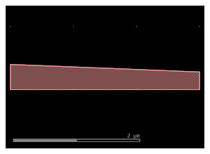
Predefined Components
Add symmetric taper and label to strip to slot
gf.CONF.plot_width, gf.CONF.plot_height = width_and_height(
    num_lines_code=11,
    max_characters_per_line=34
)
offset = 0.75*w_II + 0.25*g
# Add a predefined symmetric taper
t = gf.components.taper(
length=L,
width1=(offset-g-w_I)*2,
width2=(w_II-g)/2)
t_ref = c << t
t_ref.movey(offset)
c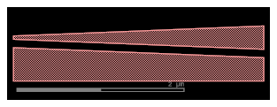
Python PCells
taper of different length (autolabeled)
def flip(c):
    wrapper = gf.Component()
    ref = wrapper << c
    ref.rotate(-90)
    return wrapper
gf.CONF.plot_width, gf.CONF.plot_height = width_and_height(
num_lines_code=23,
max_characters_per_line=53 + 30
)# The @gf.cell decorator makes this function a PCell,
# adding caching and other features.
@gf.cell
def _strip_to_slot(
w_I = 0.4, w_II = 0.66, g = 0.1, L = 3.0,
) -> gf.Component:
c = gf.Component()
c.add_polygon(
[(0, 0), (L, 0), (L, (w_II-g)/2), (0, w_I)],
layer = PDK.layers.WG
)
offset = 0.75*w_II + 0.25*g
t = gf.components.taper(length=L,
width1=(offset-g-w_I)*2, width2=(w_II-g)/2)
(c << t).movey(offset)
return c
flip(_strip_to_slot(L=4.0)) # Flip for viz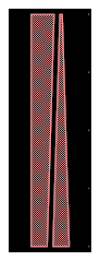
Cross Sections
gf.CONF.plot_width, gf.CONF.plot_height = width_and_height(
    num_lines_code=14,
    max_characters_per_line=53 + 30
)
w_rail = (w_II-g)/2
offset = (w_II+g)/4
s0 = gf.Section(width=w_II, offset=0, layer=PDK.layers.WG,
hidden=True, port_names=('o1', 'o2')) # Specify ports
s1 = gf.Section(width=w_rail, offset=offset, layer=PDK.layers.WG)
s2 = gf.Section(width=w_rail, offset=-offset, layer=PDK.layers.WG)
xs_slot = gf.CrossSection(sections=(s0, s1, s2))
p = gf.path.straight(4.0)
c = gf.path.extrude(p, cross_section=xs_slot)
c.draw_ports()
flip(c)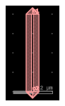
Ports
gf.CONF.plot_width, gf.CONF.plot_height = width_and_height(
    num_lines_code=30,
    max_characters_per_line=59 + 20
)
@gf.cell
def strip_to_slot(
w_I = 0.4, w_II = 0.66,
g = 0.1, L = 3.0,
) -> gf.Component:
c = gf.Component()
c << _strip_to_slot(w_I, w_II, g, L)
kwargs = dict(layer=PDK.layers.WG, port_type='optical')
c.add_port(
name='o1', width=w_I,
orientation=180, center=(0, w_I/2),
**kwargs
)
c.add_port(
name='o2', width=w_II, cross_section=xs_slot,
orientation=0, center=(L, w_II/2),
**kwargs
)
return c
I2II = strip_to_slot().copy()
I2II.draw_ports()
flip(I2II)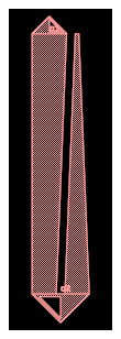
I2II.pprint_ports()# TODO why does this not work?
c = gf.Component()
p = gf.path.straight(2.0)
for i, port in enumerate(I2II.ports):
wg = gf.path.extrude(p, cross_section=port.cross_section)
(c << wg).movex(i*4)
flip(c)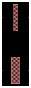
gf.CONF.plot_width, gf.CONF.plot_height = width_and_height(
    num_lines_code=22,
    max_characters_per_line=41
)
@gf.cell
def convert_and_bend() -> gf.Component:
c = gf.Component()
I2II = c << strip_to_slot(L=4.0)
bend = c << (
gf.components.bend_euler(
radius=5,
width=I2II.ports["o1"].width)
)
bend.connect("o1", I2II.ports["o1"])
c.add_port("o1", port=bend.ports["o2"])
c.add_port("o2", port=I2II.ports["o2"])
return c
c_convert_and_bend = convert_and_bend()
c_convert_and_bend.draw_ports()
flip(c_convert_and_bend)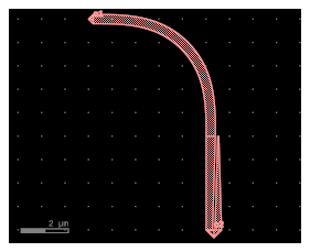
c_convert_and_bend.pprint_ports()Routing
gf.CONF.plot_width, gf.CONF.plot_height = width_and_height(
    num_lines_code=17,
    max_characters_per_line=41
)
c = gf.Component()
I2II = strip_to_slot()
c << I2II
dummy = gf.components.straight(3)
dummy_ref = c << dummy
dummy_ref.move((40, -20))
# Automatically route a single waveguide
route = gf.routing.route_single(
c,
port1=dummy_ref.ports["o1"],
port2=I2II.ports["o2"],
cross_section=gf.cross_section.strip,
)
c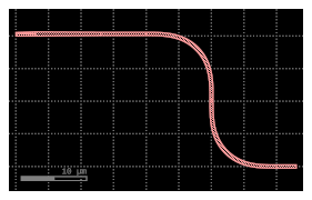
gf.CONF.plot_width, gf.CONF.plot_height = width_and_height(
    num_lines_code=21,
    max_characters_per_line=49
)
c = gf.Component()
converters = [c << I2II for _ in range(4)]
wgs = [c << dummy for _ in range(4)]
for i, conv in enumerate(converters):
conv.move((13, (i-1.5)*5))
for i, wg in enumerate(wgs):
wg.movey((i-1.5)*2)
# Automatically route a waveguide
# between the waveguides and converters
gf.routing.route_bundle_sbend(
c,
ports1=[wg.ports["o2"] for wg in wgs],
ports2=[cv.ports["o1"] for cv in converters],
cross_section=gf.cross_section.strip,
)
flip(c)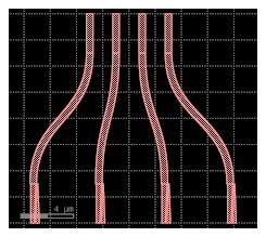
4 WGs to 4 stip to slot
YAML-flow
Pack/Grid
Regression Tests
Rev 1: fundamental comp -> derived component 1
Rev 2: fundamental comp -> derived component 1 & derived component 2
To introduce derived comp 2 the design engineer introduced changes to fundamental comp -> regression in derived comp 1 -> show GDSdiff.
Simulation
Component Level Optical Simulations
S-Parameters of a Strip to Slot Converter
S-Parameters of a Directional Coupler
S-parameters of a Grating Coupler
Component Level Electrical and Thermal Simulations
Thermal Tuners
Modulators (travelling wave)
Process Development Kits
Layer Definitions
Cross-sections; Layer Stack
Cell-library
Design Rules
Measurement and Validation
Metadata: Location of Fibercouplers; Measurement Schema; Wafer prober compatibility
Teststructures: Processcontrol; Litho/Alignment; DOE; Cutback; TLM