

PCells#
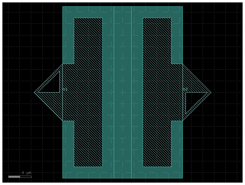
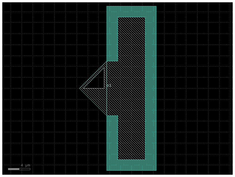
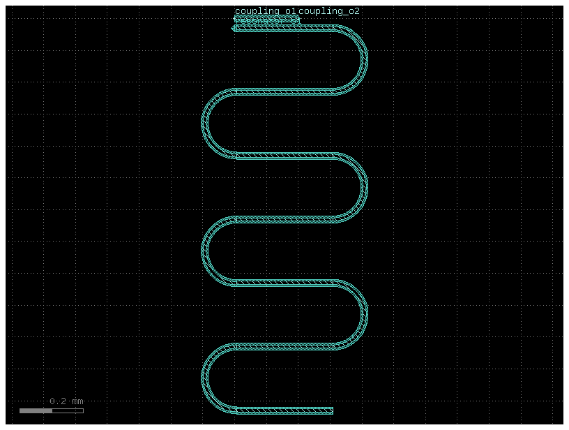
Gallery#


API Reference#
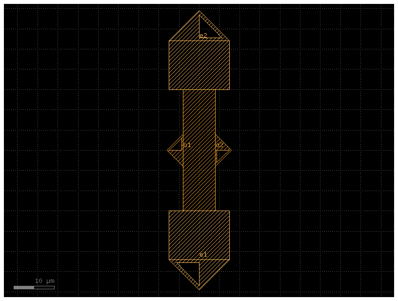
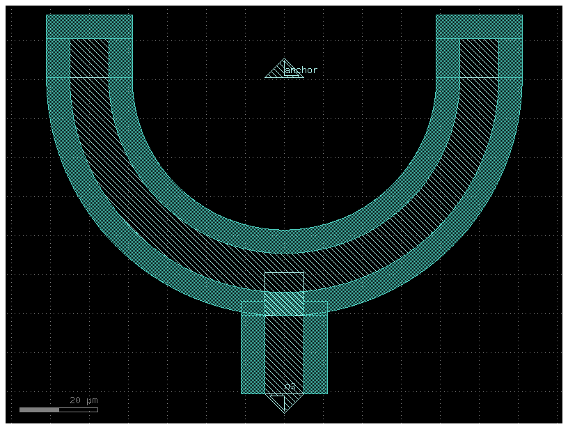
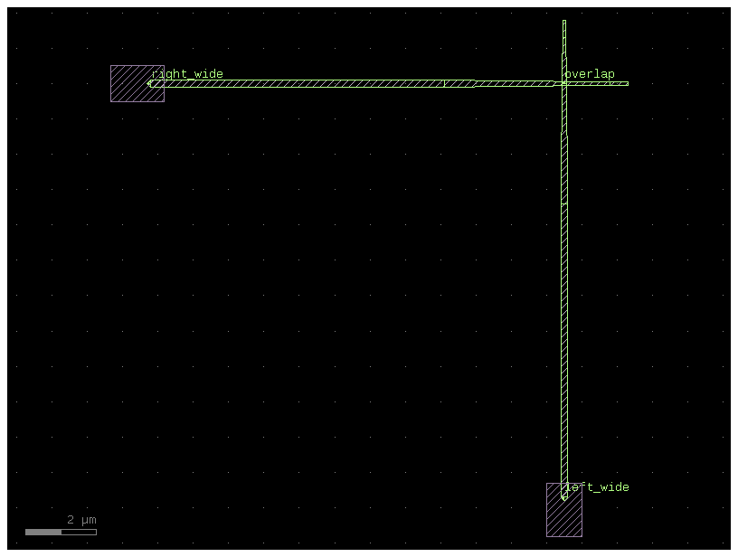
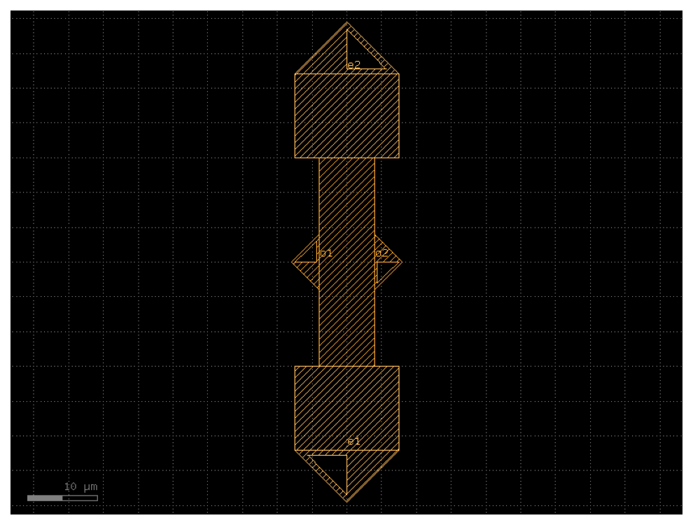
airbridge#
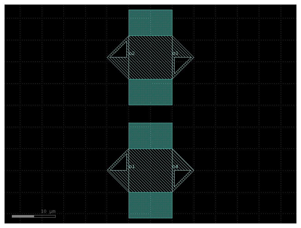
- qpdk.cells.airbridge(bridge_length=30.0, bridge_width=8.0, pad_width=15.0, pad_length=12.0, bridge_layer=<LayerMapQPDK.AB_DRAW: 49>, pad_layer=<LayerMapQPDK.AB_VIA: 50>)[source]#
Generate a superconducting airbridge component.
Creates an airbridge consisting of a suspended bridge span and landing pads on either side. The bridge allows transmission lines to cross over each other without electrical contact, which is essential for complex quantum circuit routing without crosstalk.

The bridge_layer (AB_DRAW) represents the elevated metal bridge structure, while the pad_layer (AB_VIA) represents the contact/landing pads that connect to the underlying circuit.
Note
To be used with
ComponentAlongPaththe unrotated version should be oriented for placement on a horizontal line.- Parameters:
bridge_length (float) – Total length of the airbridge span in µm.
bridge_width (float) – Width of the suspended bridge in µm.
pad_width (float) – Width of the landing pads in µm.
pad_length (float) – Length of each landing pad in µm.
bridge_layer (LayerSpec) – Layer for the suspended bridge metal (default: AB_DRAW).
pad_layer (LayerSpec) – Layer for the landing pads/contacts (default: AB_VIA).
- Returns:
Component containing the airbridge geometry with appropriate ports.
- Return type:
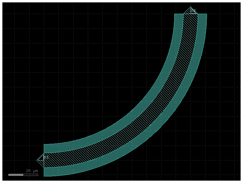
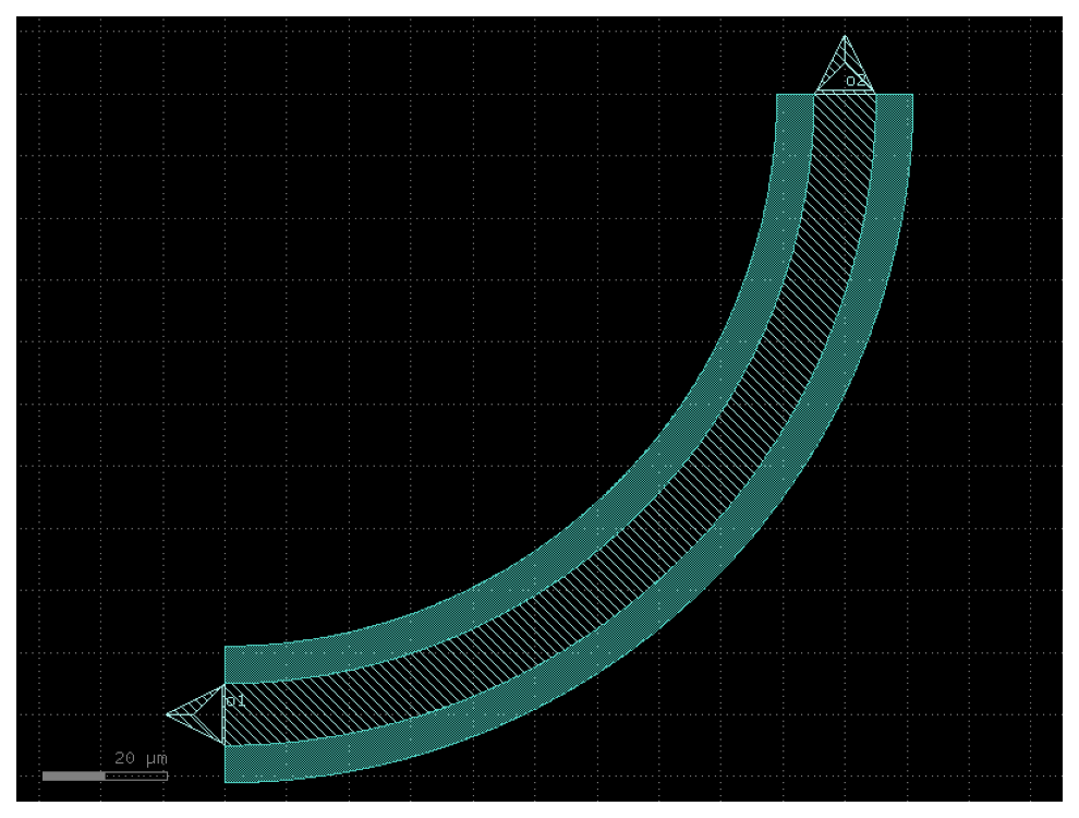
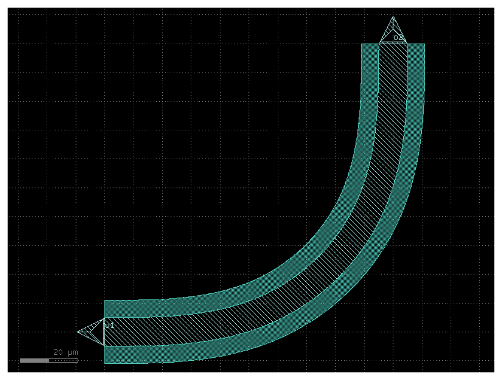
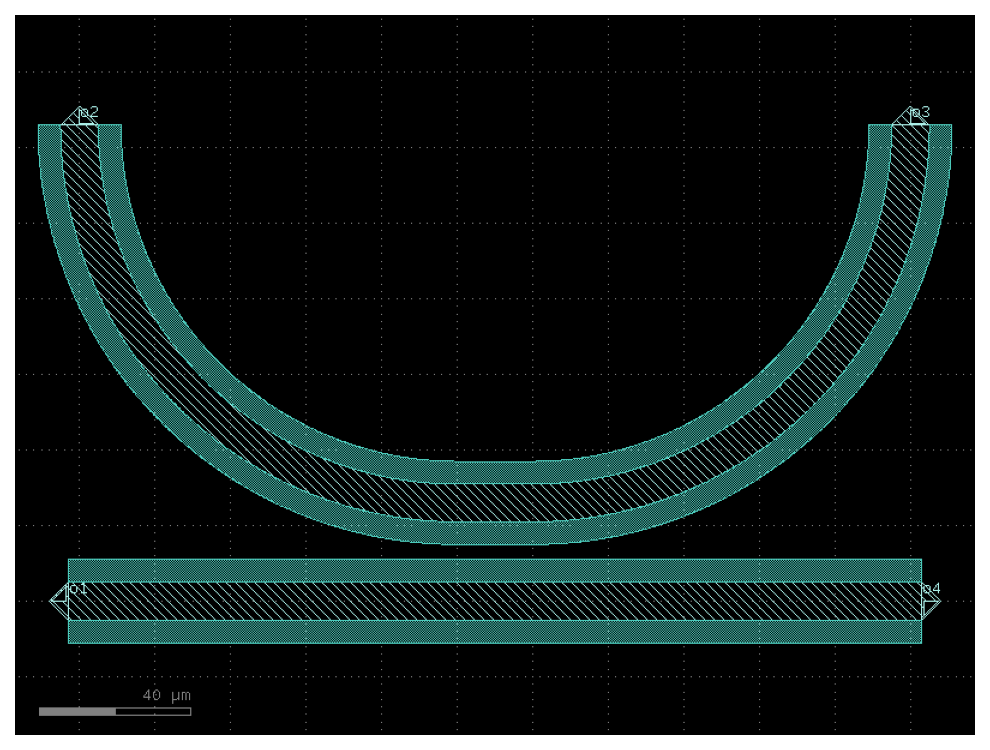
bend_circular#
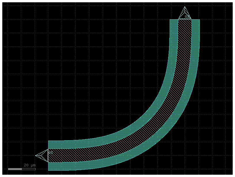
- qpdk.cells.bend_circular(angle=90.0, radius=100.0, npoints=None, cross_section=<function coplanar_waveguide>, width=None, allow_min_radius_violation=True, **kwargs)[source]#
Returns circular bend.
Cross-sections have a minimum value of allowed bend radius, which is half their total width. If the user-specified radius is smaller than this value, it is adjusted to the minimum acceptable one.
- Parameters:
angle (float) – Angle of the bend in degrees.
radius (float) – Radius of the bend in μm.
npoints (int | None) – Number of points for the bend (optional, cannot be used with angular_step).
cross_section (CrossSectionSpec) – Cross-section specification.
width (float | None) – Optional width override in μm.
allow_min_radius_violation (bool) – Allow radius smaller than cross-section radius.
**kwargs – Additional arguments passed to gf.c.bend_circular (e.g., angular_step).
- Return type:

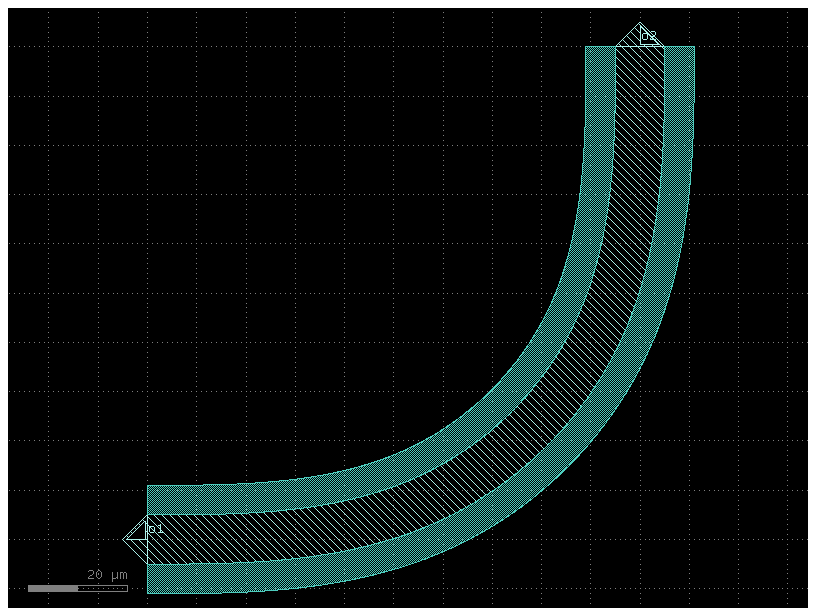
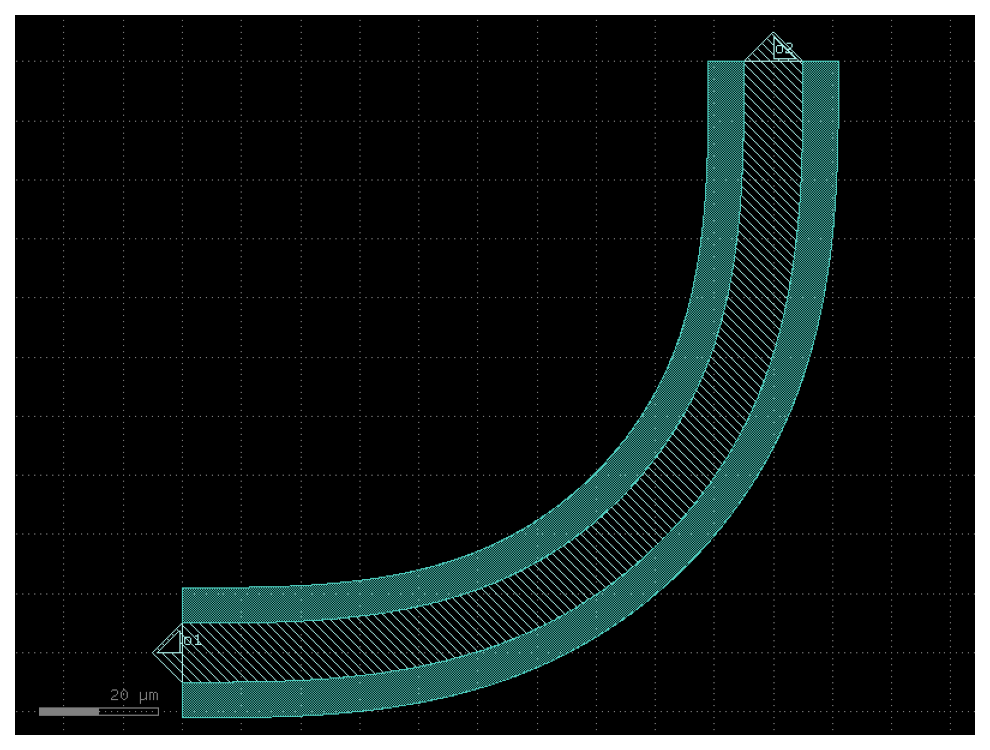
bend_circular_all_angle#
- qpdk.cells.bend_circular_all_angle(radius=100.0, angle=90.0, npoints=None, layer=None, width=None, cross_section=<function coplanar_waveguide>, allow_min_radius_violation=True)[source]#
Returns circular bend with arbitrary angle.
- Parameters:
radius (float | None) – Radius of the bend in μm.
angle (float) – Angle of the bend in degrees.
npoints (int | None) – Number of points for the bend.
layer (LayerSpec | None) – Layer specification.
width (float | None) – Optional width override in μm.
cross_section (CrossSectionSpec) – Cross-section specification.
allow_min_radius_violation (bool) – Allow radius smaller than cross-section radius.
- Return type:
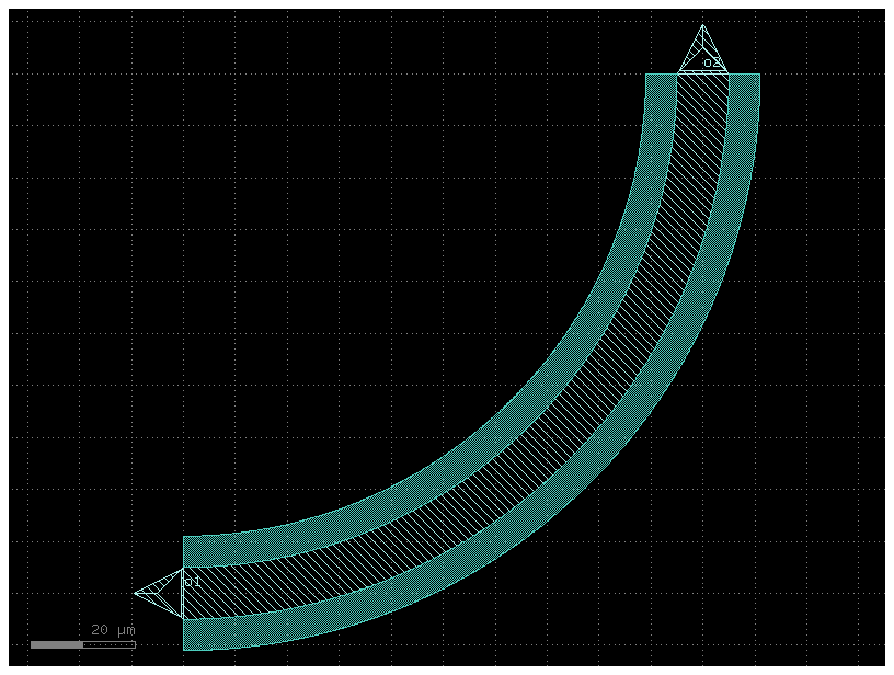
bend_euler#
- qpdk.cells.bend_euler(angle=90.0, p=0.5, with_arc_floorplan=True, npoints=720, cross_section=<function coplanar_waveguide>, allow_min_radius_violation=True, **kwargs)[source]#
Regular degree euler bend.
- Parameters:
angle (float) – Angle of the bend in degrees.
p (float) – Fraction of the bend that is curved (0-1).
with_arc_floorplan (bool) – Include arc floorplan.
npoints (int) – Number of points for the bend.
cross_section (CrossSectionSpec) – Cross-section specification.
allow_min_radius_violation (bool) – Allow radius smaller than cross-section radius.
**kwargs – Additional arguments passed to gf.c.bend_euler.
- Returns:
The euler bend component.
- Return type:
bend_euler_all_angle#
- qpdk.cells.bend_euler_all_angle(radius=None, angle=90.0, p=0.5, with_arc_floorplan=True, npoints=None, layer=None, width=None, cross_section=<function coplanar_waveguide>, allow_min_radius_violation=True)[source]#
Returns regular degree euler bend with arbitrary angle.
- Parameters:
radius (float | None) – Radius of the bend in μm.
angle (float) – Angle of the bend in degrees.
p (float) – Fraction of the bend that is curved (0-1).
with_arc_floorplan (bool) – Include arc floorplan.
npoints (int | None) – Number of points for the bend.
layer (LayerSpec | None) – Layer specification.
width (float | None) – Optional width override in μm.
cross_section (CrossSectionSpec) – Cross-section specification.
allow_min_radius_violation (bool) – Allow radius smaller than cross-section radius.
- Return type:
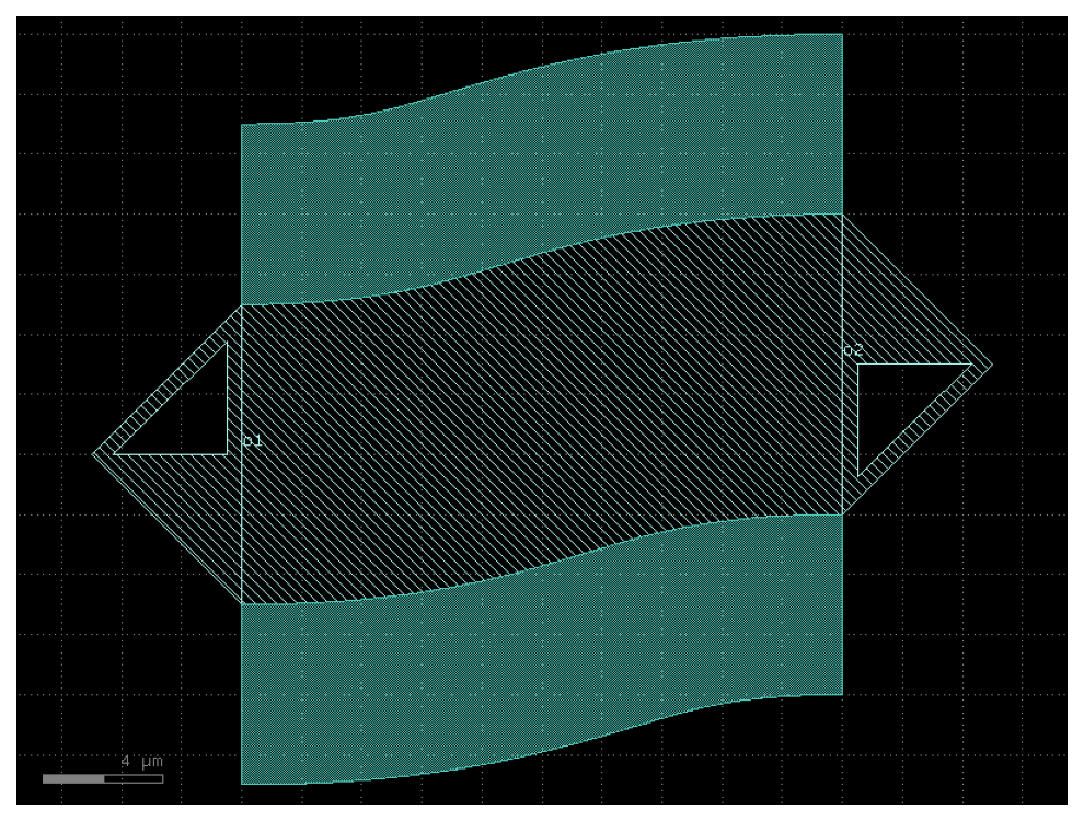
bend_s#
- qpdk.cells.bend_s(size=(20.0, 3.0), cross_section=<function coplanar_waveguide>, width=None, allow_min_radius_violation=True, **kwargs)[source]#
Return S bend with bezier curve.
stores min_bend_radius property in self.info[‘min_bend_radius’] min_bend_radius depends on height and length
- Parameters:
size (Size) – Tuple of (length, offset) for the S bend in μm.
cross_section (CrossSectionSpec) – Cross-section specification.
width (float | None) – Optional width override in μm.
allow_min_radius_violation (bool) – Allow radius smaller than cross-section radius.
**kwargs – Additional arguments passed to gf.c.bend_s.
- Return type:
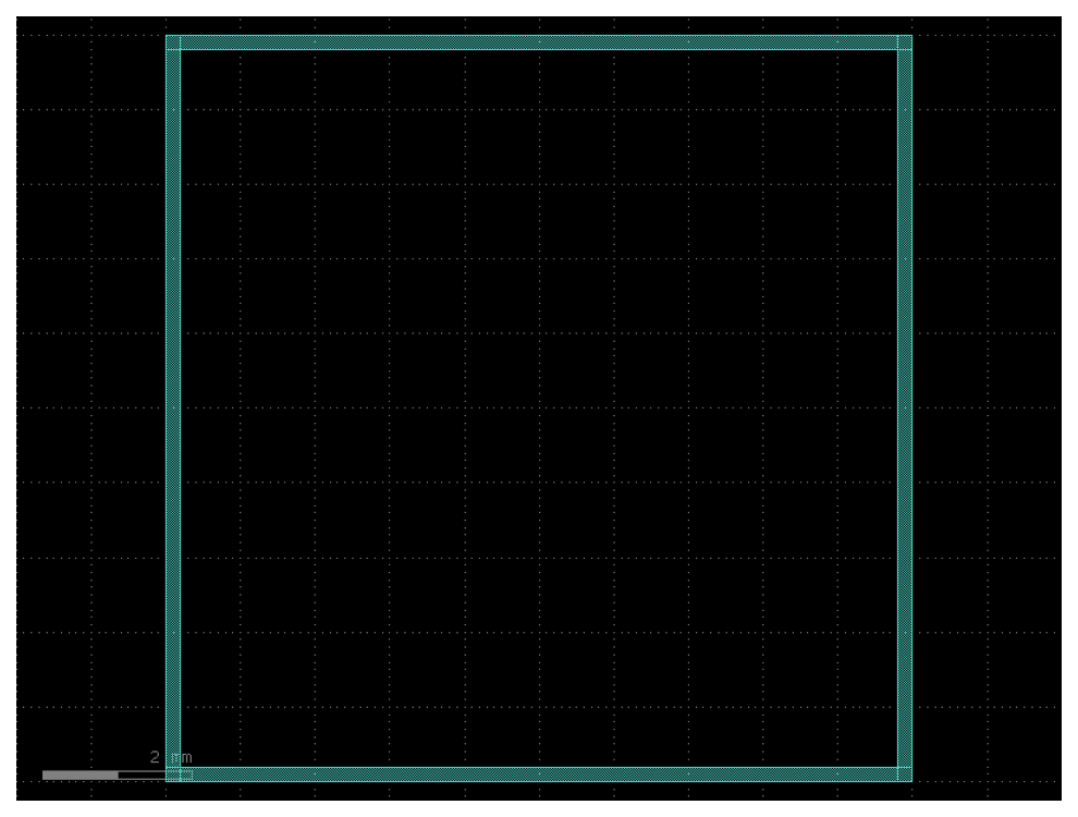
chip_edge#
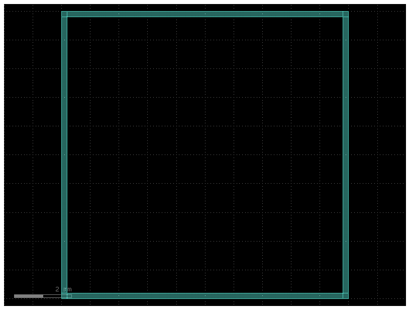
- qpdk.cells.chip_edge(size=(10000.0, 10000.0), width=200.0, layer='M1_ETCH')[source]#
Returns a chip edge component with hollow rectangle frame.
Creates a rectangular frame (hollow rectangle) on an etched metal layer, typically used to define chip edge regions for proper fabrication.
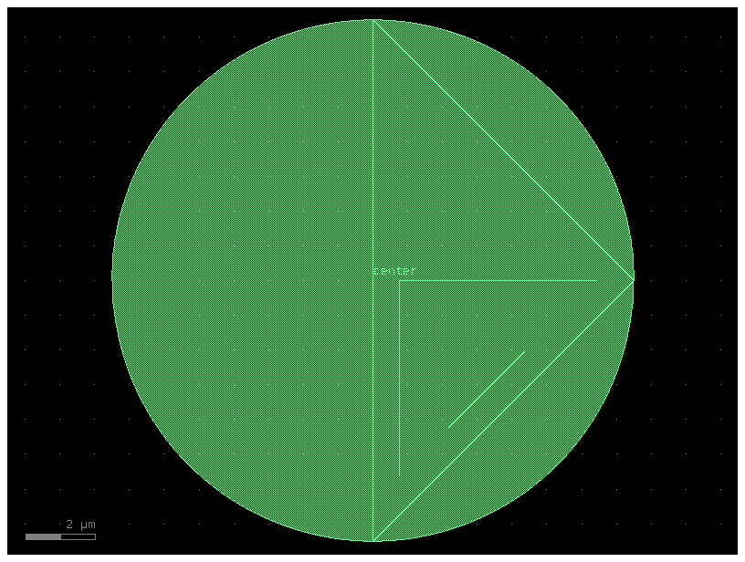
circle#
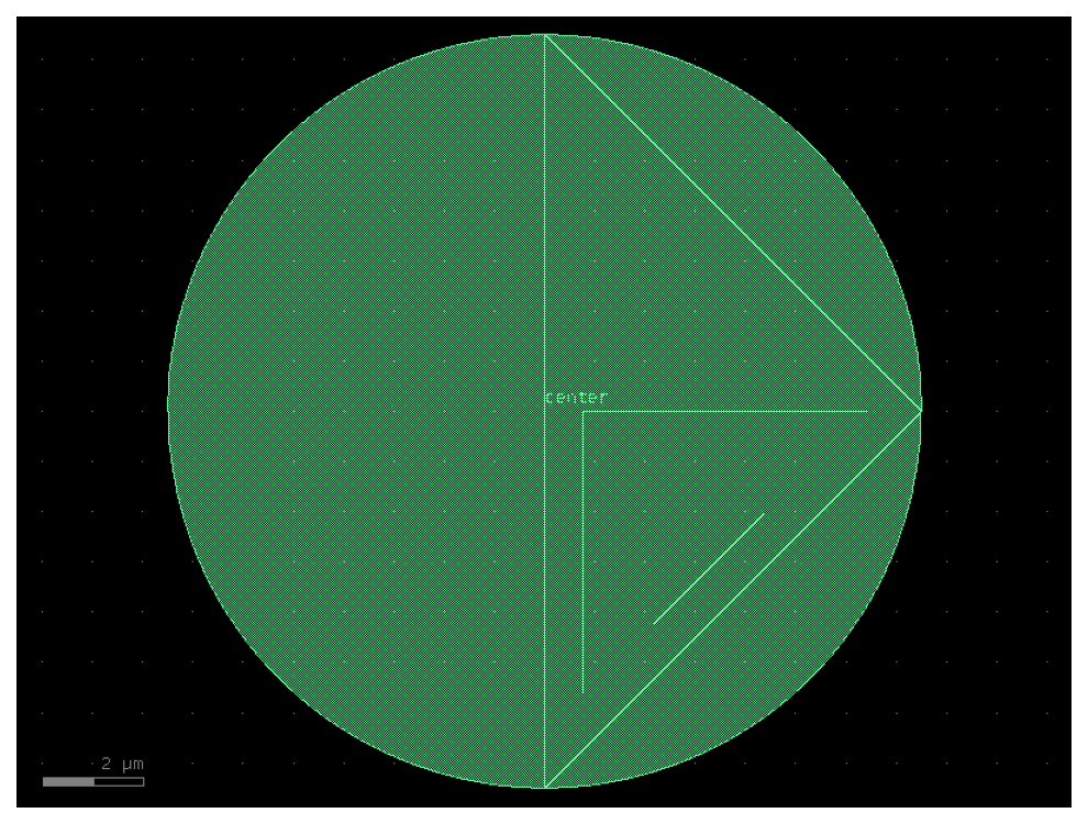
- qpdk.cells.circle(radius=10.0, angle_resolution=2.5, layer='WG')[source]#
Generate a circle geometry.
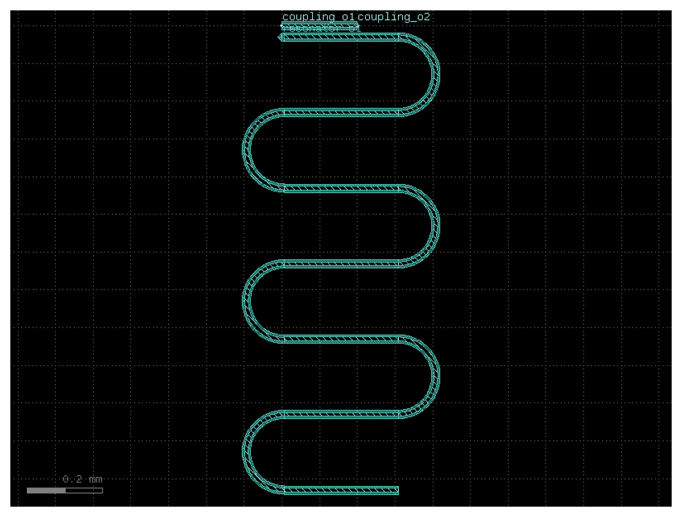
coupler_ring#
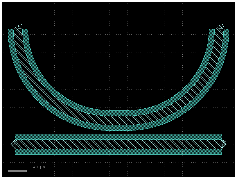
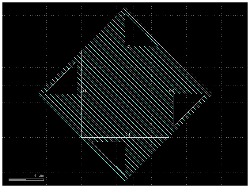
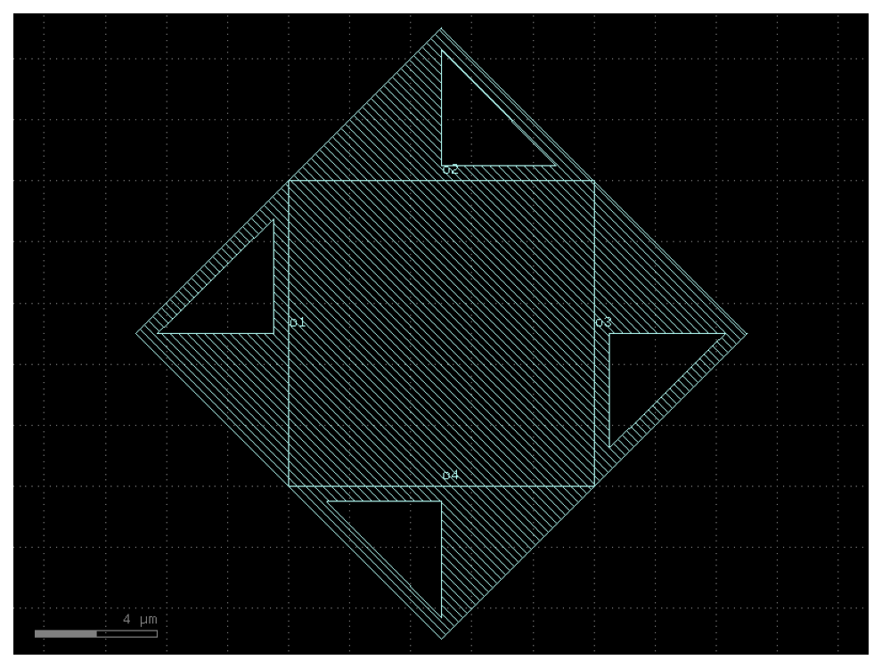
- qpdk.cells.coupler_ring(*, gap=16, radius=None, length_x=20, bend=<function bend_circular>, straight=<function straight>, cross_section='cpw', cross_section_bend=None, length_extension=None)#
Coupler for ring.
- Parameters:
gap (float) – spacing between parallel coupled straight waveguides.
radius (float | None) – of the bends. Default is None, which uses the default radius of the cross_section.
length_x (float) – length of the parallel coupled straight waveguides.
bend (ComponentSpec) – 90 degrees bend spec.
straight (ComponentSpec) – straight spec.
cross_section (CrossSectionSpec) – cross_section spec.
cross_section_bend (CrossSectionSpec | None) – optional bend cross_section spec.
length_extension (float | None) –
straight length extension at the end of the coupler bottom ports.
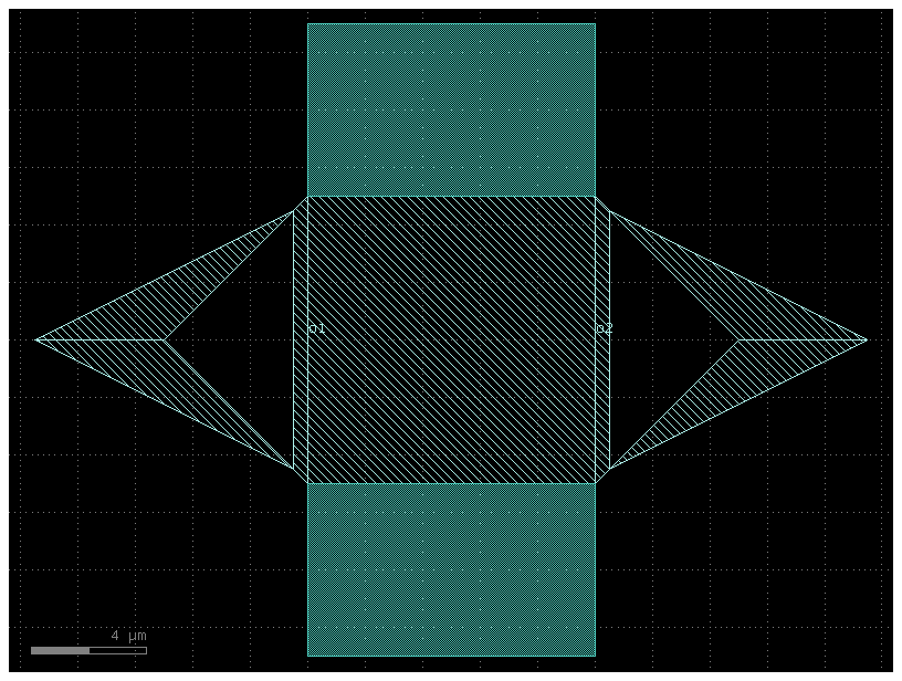
o2 o3 xx xx xx xx
- xx length_x x
- xx ◄───────────────► x
- xx xxx
- xx xxx
- xxx──────▲─────────xxx
│gap
- o1──────▼─────────◄──────────────► o4
length_extension
- Return type:
Component
coupler_straight#
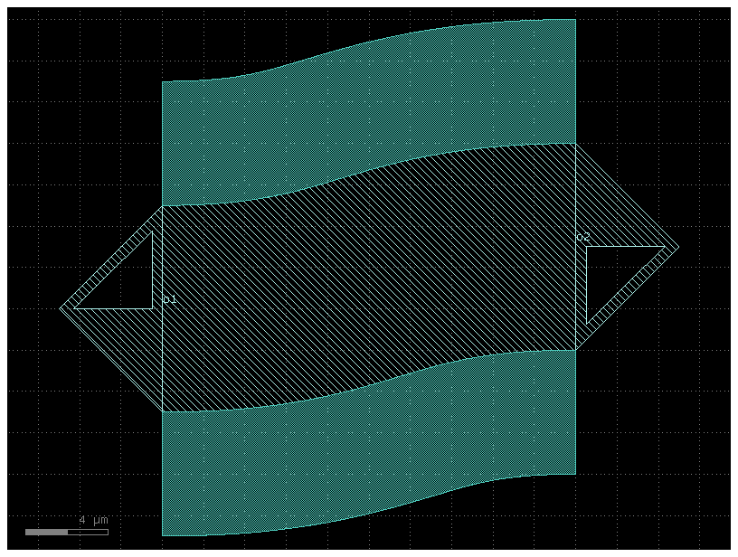
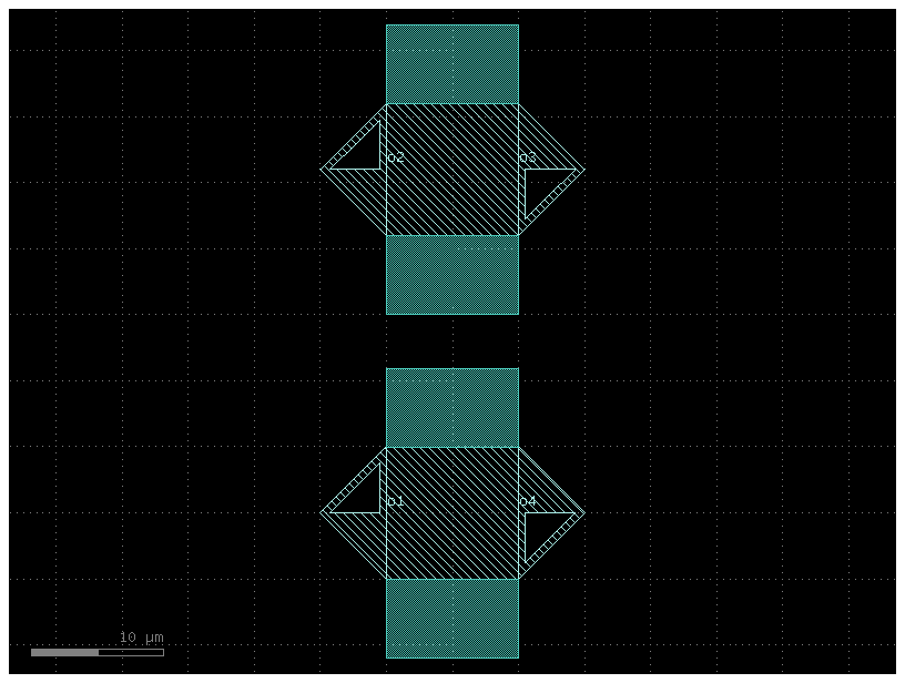
- qpdk.cells.coupler_straight(length=10.0, *, gap=16, cross_section='cpw')#
Coupler_straight with two parallel straights.
double_pad_transmon#
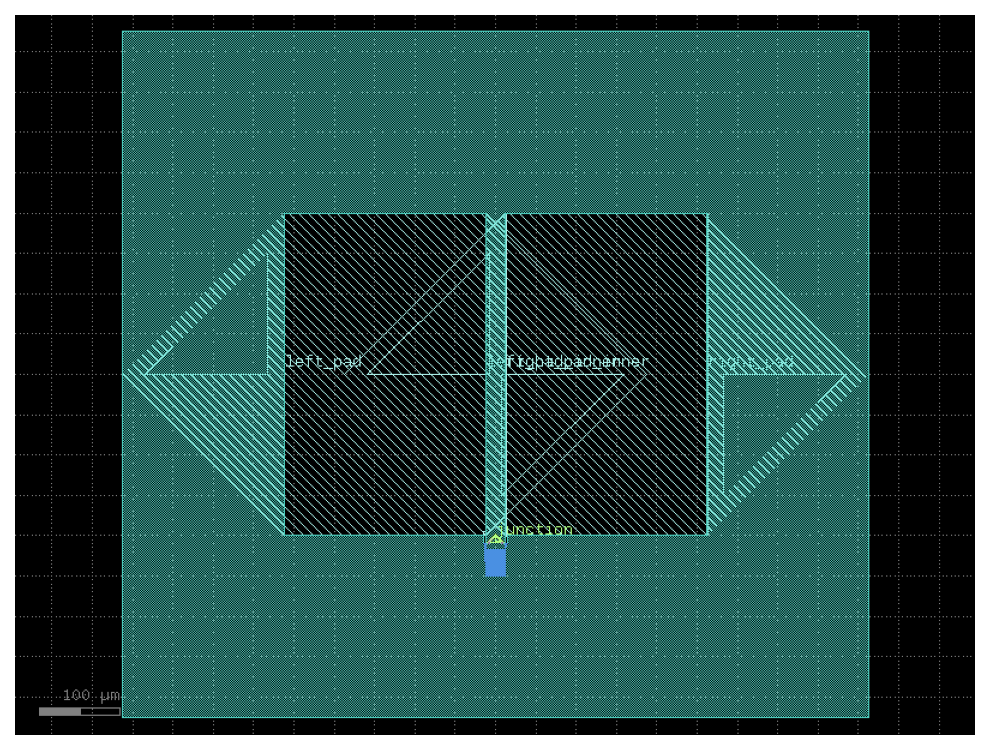
- qpdk.cells.double_pad_transmon(pad_size=(250.0, 400.0), pad_gap=15.0, junction_spec=<function squid_junction>, junction_displacement=None, layer_metal=<LayerMapQPDK.M1_DRAW: 1>)[source]#
Creates a double capacitor pad transmon qubit with Josephson junction.
A transmon qubit consists of two capacitor pads connected by a Josephson junction. The junction creates an anharmonic oscillator that can be used as a qubit.

See [KYG+07] for details.
- Parameters:
pad_size (tuple[float, float]) – (width, height) of each capacitor pad in μm.
pad_gap (float) – Gap between the two capacitor pads in μm.
junction_spec (ComponentSpec) – Component specification for the Josephson junction component.
junction_displacement (DCplxTrans | None) – Optional complex transformation to apply to the junction.
layer_metal (LayerSpec) – Layer for the metal pads.
- Returns:
A gdsfactory component with the transmon geometry.
- Return type:
Component
double_pad_transmon_with_bbox#
- qpdk.cells.double_pad_transmon_with_bbox(bbox_extension=200.0, pad_size=(250.0, 400.0), pad_gap=15.0, junction_spec=<function squid_junction>, junction_displacement=None, layer_metal=<LayerMapQPDK.M1_DRAW: 1>, layer_etch=<LayerMapQPDK.M1_ETCH: 47>)[source]#
Creates a double capacitor pad transmon qubit with Josephson junction and an etched bounding box.
See
double_pad_transmon()for more details.- Parameters:
bbox_extension (float) – Extension size for the bounding box in μm.
pad_size (tuple[float, float]) – (width, height) of each capacitor pad in μm.
pad_gap (float) – Gap between the two capacitor pads in μm.
junction_spec (ComponentSpec) – Component specification for the Josephson junction component.
junction_displacement (DCplxTrans | None) – Optional complex transformation to apply to the junction.
layer_metal (LayerSpec) – Layer for the metal pads.
layer_etch (LayerSpec) – Layer for the etched bounding box.
- Returns:
A gdsfactory component with the transmon geometry and etched box.
- Return type:
Component
double_pad_transmon_with_resonator#
- qpdk.cells.double_pad_transmon_with_resonator(*, qubit='double_pad_transmon_with_bbox', resonator=functools.partial(<function resonator>, open_start=False, open_end=True, start_with_bend=True, length=4000, meanders=6), resonator_meander_start=(-900, -1200), resonator_length=5000.0, resonator_meanders=5, resonator_bend_spec='bend_circular', resonator_cross_section='cpw', resonator_open_start=False, resonator_open_end=True, coupler=functools.partial(<function plate_capacitor_single>, width=20, length=394), qubit_rotation=90, coupler_port='left_pad', coupler_offset=(-45, 0))#
Returns a transmon qubit coupled to a quarter wave resonator.
- Parameters:
qubit (ComponentSpec) – Qubit component.
resonator (ComponentSpec) – Resonator component.
resonator_meander_start (tuple[float, float]) – (x, y) position of the start of the resonator meander.
resonator_length (float) – Length of the resonator in µm.
resonator_meanders (int) – Number of meander sections for the resonator.
resonator_bend_spec (ComponentSpec) – Specification for the bend component used in meanders.
resonator_cross_section (CrossSectionSpec) – Cross-section specification for the resonator.
resonator_open_start (bool) – If True, adds an etch section at the start of the resonator.
resonator_open_end (bool) – If True, adds an etch section at the end of the resonator.
coupler (ComponentSpec) – Coupler spec.
qubit_rotation (float) – Rotation angle for the qubit in degrees.
coupler_port (str) – Name of the qubit port to position the coupler relative to.
coupler_offset (tuple[float, float]) – (x, y) offset for the coupler position.
- Return type:
Component

double_pad_transmon_with_resonator_and_probeline#
- qpdk.cells.double_pad_transmon_with_resonator_and_probeline(*, qubit='double_pad_transmon_with_bbox', resonator=functools.partial(<function resonator>, open_start=False, open_end=True, start_with_bend=True, length=4000, meanders=6), resonator_meander_start=(-900, -1200), resonator_length=5000.0, resonator_meanders=5, resonator_bend_spec='bend_circular', resonator_cross_section='cpw', resonator_open_start=False, resonator_open_end=True, coupler=functools.partial(<function plate_capacitor_single>, width=20, length=394), qubit_rotation=90, coupler_port='left_pad', coupler_offset=(-45, 0), probeline_coupler=functools.partial(<function coupler_straight>, cross_section='cpw', gap=16), probeline_coupling_gap=16.0, probeline_coupling_length=None)#
Returns a transmon qubit coupled to a quarter wave resonator and a probeline.
Uses a
coupler_straight()to couple the resonator to a probeline. The coupling section is inserted at the start of the resonator meander, with one waveguide carrying the resonator signal and the other providing ports for probeline routing.- Parameters:
qubit (ComponentSpec) – Qubit component.
resonator (ComponentSpec) – Resonator component.
resonator_meander_start (tuple[float, float]) – (x, y) position of the start of the resonator meander.
resonator_length (float) – Length of the resonator in µm.
resonator_meanders (int) – Number of meander sections for the resonator.
resonator_bend_spec (ComponentSpec) – Specification for the bend component used in meanders.
resonator_cross_section (CrossSectionSpec) – Cross-section specification for the resonator.
resonator_open_start (bool) – If True, adds an etch section at the start of the resonator.
resonator_open_end (bool) – If True, adds an etch section at the end of the resonator.
coupler (ComponentSpec) – Coupler spec.
qubit_rotation (float) – Rotation angle for the qubit in degrees.
coupler_port (str) – Name of the qubit port to position the coupler relative to.
coupler_offset (tuple[float, float]) – (x, y) offset for the coupler position.
probeline_coupler (ComponentSpec) – Component spec for the probeline coupling section.
probeline_coupling_gap (float) – Gap between the resonator and probeline waveguides in the coupling section in µm.
probeline_coupling_length (float | None) – Length of the coupling section in µm.
- Return type:
Component

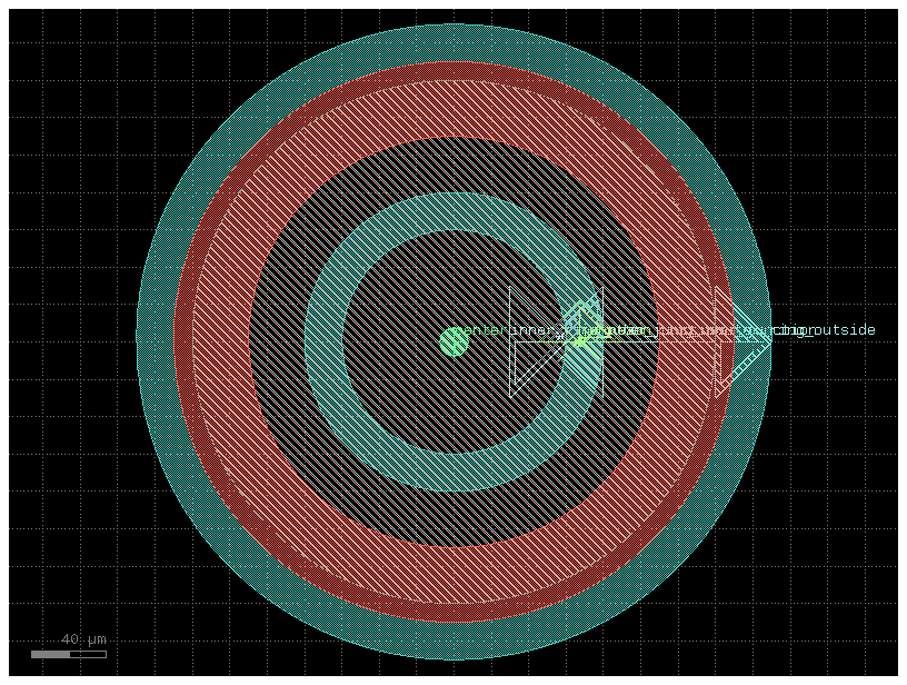
flipmon#
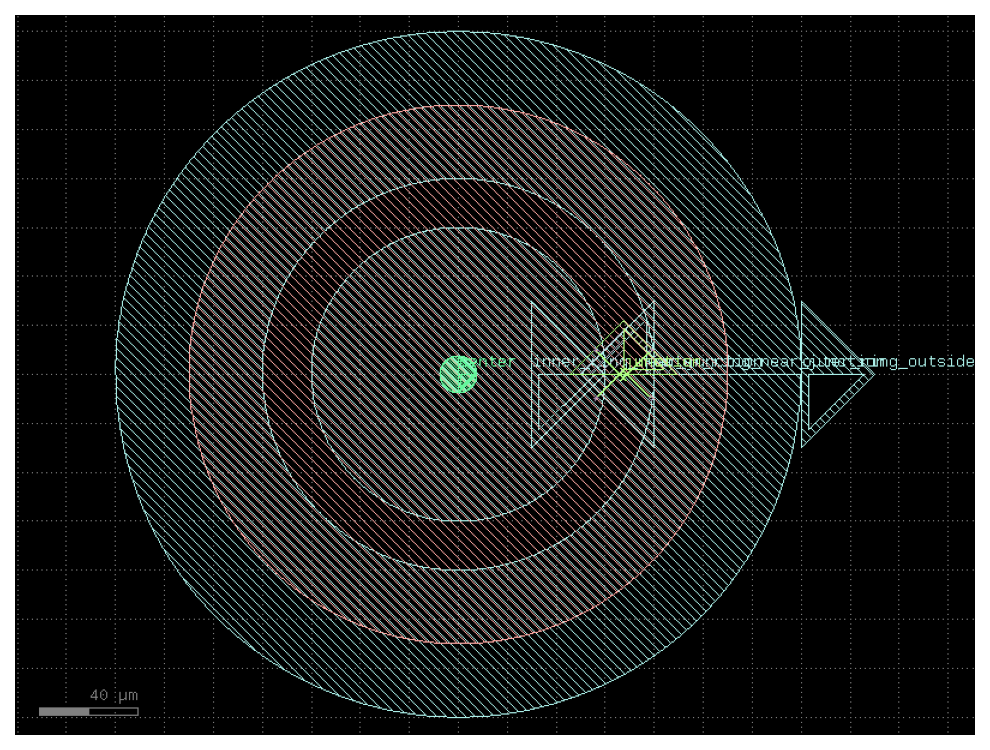
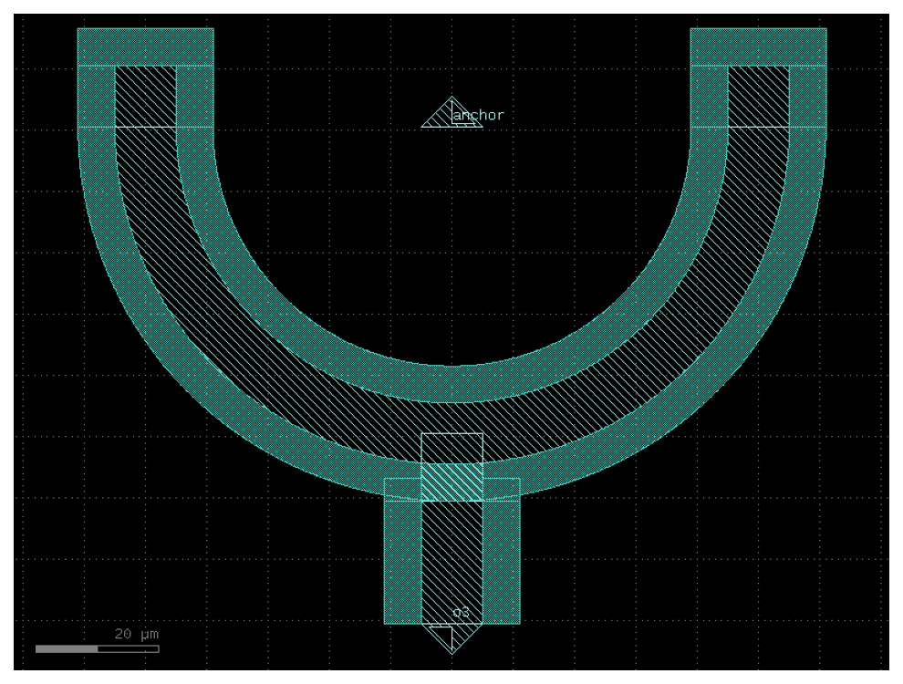
- qpdk.cells.flipmon(inner_circle_radius=60.0, outer_ring_radius=110.0, outer_ring_width=60.0, top_circle_radius=110.0, junction_spec=<function squid_junction_long>, junction_displacement=None, layer_metal=<LayerMapQPDK.M1_DRAW: 1>, layer_metal_top=<LayerMapQPDK.M2_DRAW: 3>)[source]#
Creates a circular transmon qubit with flipmon geometry.
A circular variant of the transmon qubit with another circle as the inner pad.

See [LWJ+25, LZY+21] for details about the flipmon design.
- Parameters:
inner_circle_radius (float) – Central radius of the inner circular capacitor pad in μm.
outer_ring_radius (float) – Central radius of the outer circular capacitor pad in μm.
outer_ring_width (float) – Width of the outer circular capacitor pad in μm.
top_circle_radius (float) – Central radius of the top circular capacitor pad in μm. There is no separate width as the filled circle is not a ring.
junction_spec (ComponentSpec) – Component specification for the Josephson junction component.
junction_displacement (DCplxTrans | None) – Optional complex transformation to apply to the junction.
layer_metal (LayerSpec) – Layer for the metal pads.
layer_metal_top (LayerSpec) – Layer for the other metal layer pad for flip-chip.
- Returns:
A gdsfactory component with the circular transmon geometry.
- Return type:
Component
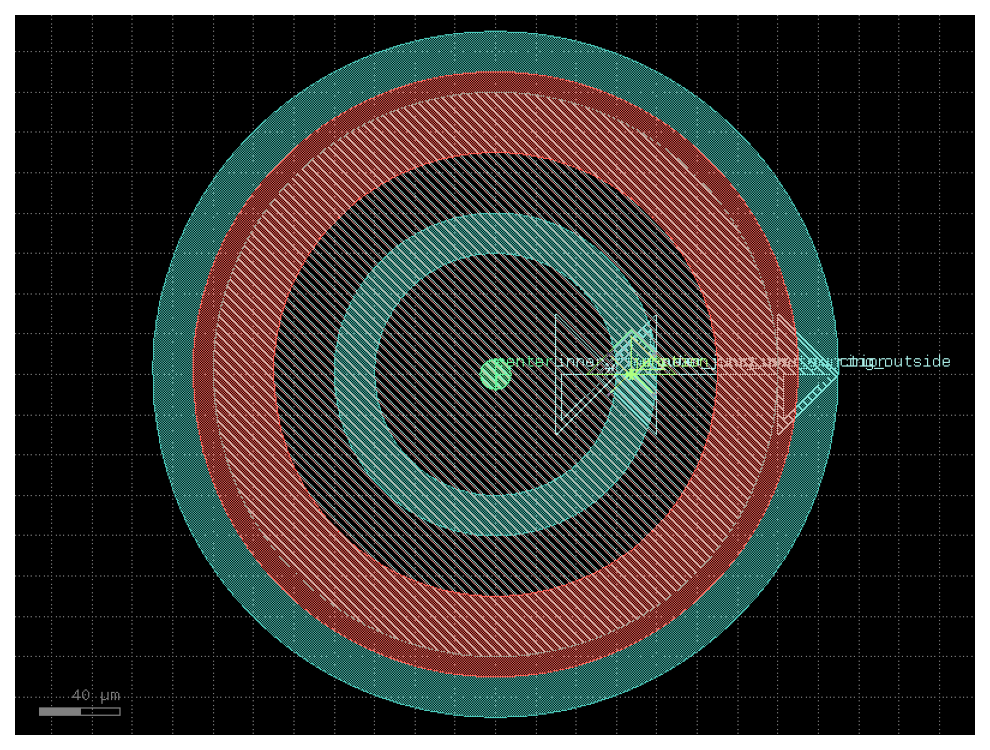
flipmon_with_bbox#
- qpdk.cells.flipmon_with_bbox(inner_circle_radius=60.0, outer_ring_radius=110.0, outer_ring_width=60.0, top_circle_radius=110.0, junction_spec=<function squid_junction_long>, junction_displacement=None, layer_metal=<LayerMapQPDK.M1_DRAW: 1>, layer_metal_top=<LayerMapQPDK.M2_DRAW: 3>, layer_etch=<LayerMapQPDK.M1_ETCH: 47>, layer_etch_top=<LayerMapQPDK.M2_ETCH: 48>, m1_etch_extension_gap=30.0, m2_etch_extension_gap=40.0)[source]#
Creates a circular transmon qubit with flipmon geometry and a circular etched bounding box.
See
flipmon()for more details.- Parameters:
inner_circle_radius (float) – Central radius of the inner circular capacitor pad in μm.
outer_ring_radius (float) – Central radius of the outer circular capacitor pad in μm.
outer_ring_width (float) – Width of the outer circular capacitor pad in μm.
top_circle_radius (float) – Central radius of the top circular capacitor pad in μm.
junction_spec (ComponentSpec) – Component specification for the Josephson junction component.
junction_displacement (DCplxTrans | None) – Optional complex transformation to apply to the junction.
layer_metal (LayerSpec) – Layer for the metal pads.
layer_metal_top (LayerSpec) – Layer for the other metal layer pad for flip-chip.
layer_etch (LayerSpec) – Layer for the M1 etched bounding box.
layer_etch_top (LayerSpec) – Layer for the M2 etched bounding box.
m1_etch_extension_gap (float) – Radius extension length for the M1 etch bounding box in μm.
m2_etch_extension_gap (float) – Radius extension length for the M2 etch bounding box in μm.
- Returns:
A gdsfactory component with the flipmon geometry and etched box.
- Return type:
Component
flipmon_with_resonator#
- qpdk.cells.flipmon_with_resonator(*, qubit='flipmon_with_bbox', resonator=functools.partial(<function resonator>, open_start=False, open_end=True, start_with_bend=True, length=4000, meanders=6), resonator_meander_start=(-900, -1200), resonator_length=5000.0, resonator_meanders=5, resonator_bend_spec='bend_circular', resonator_cross_section='cpw', resonator_open_start=False, resonator_open_end=True, coupler=functools.partial(<function plate_capacitor_single>, width=10, length=58), qubit_rotation=-90, coupler_port='outer_ring_outside', coupler_offset=(-10, 0))#
Returns a transmon qubit coupled to a quarter wave resonator.
- Parameters:
qubit (ComponentSpec) – Qubit component.
resonator (ComponentSpec) – Resonator component.
resonator_meander_start (tuple[float, float]) – (x, y) position of the start of the resonator meander.
resonator_length (float) – Length of the resonator in µm.
resonator_meanders (int) – Number of meander sections for the resonator.
resonator_bend_spec (ComponentSpec) – Specification for the bend component used in meanders.
resonator_cross_section (CrossSectionSpec) – Cross-section specification for the resonator.
resonator_open_start (bool) – If True, adds an etch section at the start of the resonator.
resonator_open_end (bool) – If True, adds an etch section at the end of the resonator.
coupler (ComponentSpec) – Coupler spec.
qubit_rotation (float) – Rotation angle for the qubit in degrees.
coupler_port (str) – Name of the qubit port to position the coupler relative to.
coupler_offset (tuple[float, float]) – (x, y) offset for the coupler position.
- Return type:
Component
flipmon_with_resonator_and_probeline#
- qpdk.cells.flipmon_with_resonator_and_probeline(*, qubit='flipmon_with_bbox', resonator=functools.partial(<function resonator>, open_start=False, open_end=True, start_with_bend=True, length=4000, meanders=6), resonator_meander_start=(-900, -1200), resonator_length=5000.0, resonator_meanders=5, resonator_bend_spec='bend_circular', resonator_cross_section='cpw', resonator_open_start=False, resonator_open_end=True, coupler=functools.partial(<function plate_capacitor_single>, width=10, length=58), qubit_rotation=-90, coupler_port='outer_ring_outside', coupler_offset=(-10, 0), probeline_coupler=functools.partial(<function coupler_straight>, cross_section='cpw', gap=16), probeline_coupling_gap=16.0, probeline_coupling_length=None)#
Returns a transmon qubit coupled to a quarter wave resonator and a probeline.
Uses a
coupler_straight()to couple the resonator to a probeline. The coupling section is inserted at the start of the resonator meander, with one waveguide carrying the resonator signal and the other providing ports for probeline routing.- Parameters:
qubit (ComponentSpec) – Qubit component.
resonator (ComponentSpec) – Resonator component.
resonator_meander_start (tuple[float, float]) – (x, y) position of the start of the resonator meander.
resonator_length (float) – Length of the resonator in µm.
resonator_meanders (int) – Number of meander sections for the resonator.
resonator_bend_spec (ComponentSpec) – Specification for the bend component used in meanders.
resonator_cross_section (CrossSectionSpec) – Cross-section specification for the resonator.
resonator_open_start (bool) – If True, adds an etch section at the start of the resonator.
resonator_open_end (bool) – If True, adds an etch section at the end of the resonator.
coupler (ComponentSpec) – Coupler spec.
qubit_rotation (float) – Rotation angle for the qubit in degrees.
coupler_port (str) – Name of the qubit port to position the coupler relative to.
coupler_offset (tuple[float, float]) – (x, y) offset for the coupler position.
probeline_coupler (ComponentSpec) – Component spec for the probeline coupling section.
probeline_coupling_gap (float) – Gap between the resonator and probeline waveguides in the coupling section in µm.
probeline_coupling_length (float | None) – Length of the coupling section in µm.
- Return type:
Component

fluxonium#
- qpdk.cells.fluxonium(pad_size=(250.0, 400.0), pad_gap=25.0, junction_spec=<function josephson_junction>, junction_displacement=None, junction_margin=1.0, inductor_n_turns=155, inductor_margin_x=1.0, inductor_cross_section=<function superinductor_cross_section>, connection_wire_width=2.0, layer_metal=<LayerMapQPDK.M1_DRAW: 1>)[source]#
Creates a fluxonium qubit with capacitor pads, Josephson junction, and superinductor.

- Parameters:
pad_size (tuple[float, float]) – (width, height) of each capacitor pad in µm.
pad_gap (float) – Gap between the two capacitor pads in µm.
junction_spec (ComponentSpec) – Component specification for the Josephson junction.
junction_displacement (DCplxTrans | None) – Optional transformation applied to the junction.
junction_margin (float) – Vertical margin between the junction and capacitor pads in µm.
inductor_n_turns (int) – Number of horizontal meander runs. Must be odd.
inductor_margin_x (float) – Horizontal margin for the inductor in µm.
inductor_cross_section (CrossSectionSpec) – Cross-section for the meander inductor.
connection_wire_width (float) – Width of the connecting wires in µm.
layer_metal (LayerSpec) – Layer for the metal pads and connection wires.
- Returns:
The fluxonium component.
- Raises:
ValueError – If inductor_n_turns is even or if pad_gap is too small.
- Return type:
fluxonium_with_bbox#
- qpdk.cells.fluxonium_with_bbox(bbox_extension=200.0, pad_size=(250.0, 400.0), pad_gap=25.0, junction_spec=<function josephson_junction>, junction_displacement=None, junction_margin=1.0, inductor_n_turns=155, inductor_margin_x=1.0, inductor_cross_section=<function superinductor_cross_section>, connection_wire_width=2.0, layer_metal=<LayerMapQPDK.M1_DRAW: 1>)[source]#
Fluxonium with an etched bounding box.
- Parameters:
bbox_extension (float) – Extension of the bounding box from the fluxonium edge in µm.
pad_size (tuple[float, float]) – (width, height) of each capacitor pad in µm.
pad_gap (float) – Gap between the two capacitor pads in µm.
junction_spec (ComponentSpec) – Component specification for the Josephson junction.
junction_displacement (DCplxTrans | None) – Optional transformation applied to the junction.
junction_margin (float) – Vertical margin between the junction and capacitor pads in µm.
inductor_n_turns (int) – Number of horizontal meander runs. Must be odd.
inductor_margin_x (float) – Horizontal margin for the inductor in µm.
inductor_cross_section (CrossSectionSpec) – Cross-section for the meander inductor.
connection_wire_width (float) – Width of the connecting wires in µm.
layer_metal (LayerSpec) – Layer for the metal pads and connection wires.
- Returns:
The fluxonium component with a bounding box.
- Return type:
half_circle_coupler#
- qpdk.cells.half_circle_coupler(radius=50.0, angle=180.0, extension_length=10.0, cross_section='cpw', extra_straight_length=20.0, open_end=True)[source]#
Creates a half-circle coupler for readout.
This coupler consists of a circular bend (typically 180 degrees) that wraps around a resonator arm for capacitive coupling.
- Parameters:
radius (float) – Inner radius of the half-circle in μm.
angle (float) – Angle of the circular arc in degrees.
extension_length (float) – Length of the straight sections extending from the ends of the half-circle in μm.
cross_section (CrossSectionSpec) – Cross-section specification for the coupler.
extra_straight_length (float) – Length of the straight section extending from the bottom of the half-circle in μm.
open_end (bool) – If True, adds an etched gap at the ends of the extensions.
- Returns:
A gdsfactory component with the half-circle coupler geometry.
- Return type:
Component
indium_bump#
- qpdk.cells.indium_bump(diameter=15.0)[source]#
Creates an indium bump component for 3D integration.
See [RKD+17] for details.
interdigital_capacitor#
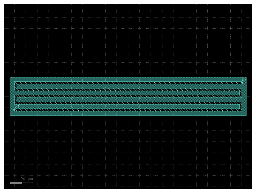
- qpdk.cells.interdigital_capacitor(fingers=4, finger_length=20.0, finger_gap=2.0, thickness=5.0, layer_metal=<LayerMapQPDK.M1_DRAW: 1>, etch_layer='M1_ETCH', etch_bbox_margin=2.0, cross_section='cpw', half=False)[source]#
Generate an interdigital capacitor component with ports on both ends.
An interdigital capacitor consists of interleaved metal fingers that create a distributed capacitance. This component creates a planar capacitor with two sets of interleaved fingers extending from opposite ends.

See for example [LeiZhuW00].
Note
finger_length=0effectively provides a parallel plate capacitor. The capacitance scales approximately linearly with the number of fingers and finger length.- Parameters:
fingers (int) – Total number of fingers of the capacitor (must be >= 1).
finger_length (float) – Length of each finger in μm.
finger_gap (float) – Gap between adjacent fingers in μm.
thickness (float) – Thickness of fingers and the base section in μm.
layer_metal (LayerSpec) – Layer for the metal fingers.
etch_layer (TypeAliasForwardRef('LayerSpec') | None) – Optional layer for etching around the capacitor.
etch_bbox_margin (float) – Margin around the capacitor for the etch layer in μm.
cross_section (CrossSectionSpec) – Cross-section for the short straight from the etch box capacitor.
half (bool) – If True, creates a single-sided capacitor (half of the interdigital capacitor).
- Returns:
- A gdsfactory component with the interdigital capacitor geometry
and two ports (‘o1’ and ‘o2’) on opposing sides.
- Return type:
Component
- Raises:
ValueError – If fingers is less than 1.
josephson_junction#
- qpdk.cells.josephson_junction(junction_overlap_displacement=1.8, wide_straight_length=8.3, narrow_straight_length=0.5, taper_length=4.7, cross_section_wide=<function josephson_junction_cross_section_wide>, cross_section_narrow=<function josephson_junction_cross_section_narrow>, layer_patch=<LayerMapQPDK.JJ_PATCH: 51>, size_patch=(1.5, 1.0))[source]#
Creates a single Josephson junction component.
A Josephson junction consists of two superconducting electrodes separated by a thin insulating barrier allowing tunnelling.

- Parameters:
junction_overlap_displacement (float) – Displacement of the overlap region in µm. Measured from the centers of the junction ports.
wide_straight_length (float) – Length of the wide straight section in µm.
narrow_straight_length (float) – Length of the narrow straight section in µm.
taper_length (float) – Length of the taper section in µm.
cross_section_wide (CrossSectionSpec) – Cross-section specification for the wide section.
cross_section_narrow (CrossSectionSpec) – Cross-section specification for the narrow section.
layer_patch (LayerSpec) – Layer for the patch that creates the overlap region.
size_patch (tuple[float, float]) – Size of the patch that creates the overlap region.
- Returns:
The Josephson junction component.
- Return type:
josephson_junction_long#
- qpdk.cells.josephson_junction_long(**kwargs)[source]#
Josephson junction with wide_straight_length=12.
- Returns:
The Josephson junction component with long wires.
- Return type:
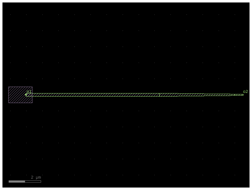
launcher#
- qpdk.cells.launcher(straight_length=200.0, taper_length=100.0, cross_section_big=<function launcher_cross_section_big>, cross_section_small='cpw')[source]#
Generate an RF launcher pad for wirebonding or probe testing.
Creates a launcher component consisting of a straight section with large cross-section connected to a tapered transition down to a smaller cross-section. This design facilitates RF signal access through probes or wirebonds while maintaining good impedance matching.

The default dimensions are taken from [TSKivijarvi+25].
- Parameters:
straight_length (float) – Length of the straight, wirebond landing area, section in µm.
taper_length (float) – Length of the taper section in µm.
cross_section_big (CrossSectionSpec) – Cross-section specification for the large end of the launcher (probe/wirebond interface).
cross_section_small (CrossSectionSpec) – Cross-section specification for the small end of the launcher (circuit interface).
- Returns:
- A gdsfactory component containing the complete launcher
geometry with one output port (“o1”) at the small end.
- Return type:
Component
lumped_element_resonator#
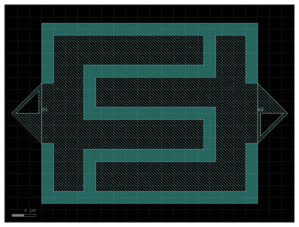
- qpdk.cells.lumped_element_resonator(fingers=20, finger_length=20.0, finger_gap=2.0, finger_thickness=5.0, n_turns=15, bus_bar_spacing=4.0, cross_section=<function meander_inductor_cross_section>, etch_bbox_margin=2.0)[source]#
Creates a lumped-element resonator combining an interdigital capacitor and a meander inductor.
The resonator consists of an interdigital capacitor section (providing capacitance) connected in parallel with a meander inductor section (providing inductance) via shared bus bars. The resonance frequency is:
\[f_r = \frac{1}{2\pi\sqrt{LC}}\]
- o1 –+ (IDC) +– o2
-
Similar structures are described in [CSD+23, KVH+11].
- Parameters:
fingers (int) – Number of interdigital capacitor fingers.
finger_length (float) – Length of each capacitor finger in µm.
finger_gap (float) – Gap between adjacent capacitor fingers in µm.
finger_thickness (float) – Width of each capacitor finger and bus bar in µm.
n_turns (int) – Number of horizontal meander inductor runs.
bus_bar_spacing (float) – Vertical spacing between the capacitor and inductor sections in µm.
cross_section (CrossSectionSpec) – Cross-section specification for the inductor and ports.
etch_bbox_margin (float) – Margin around the structure for the etch region in µm.
- Returns:
- A gdsfactory component with the lumped-element resonator
geometry and two ports (‘o1’ and ‘o2’).
- Return type:
Component
- Raises:
ValueError – If n_turns is even, bus_bar_spacing <= 0, or if the resultant meander run length is non-positive.
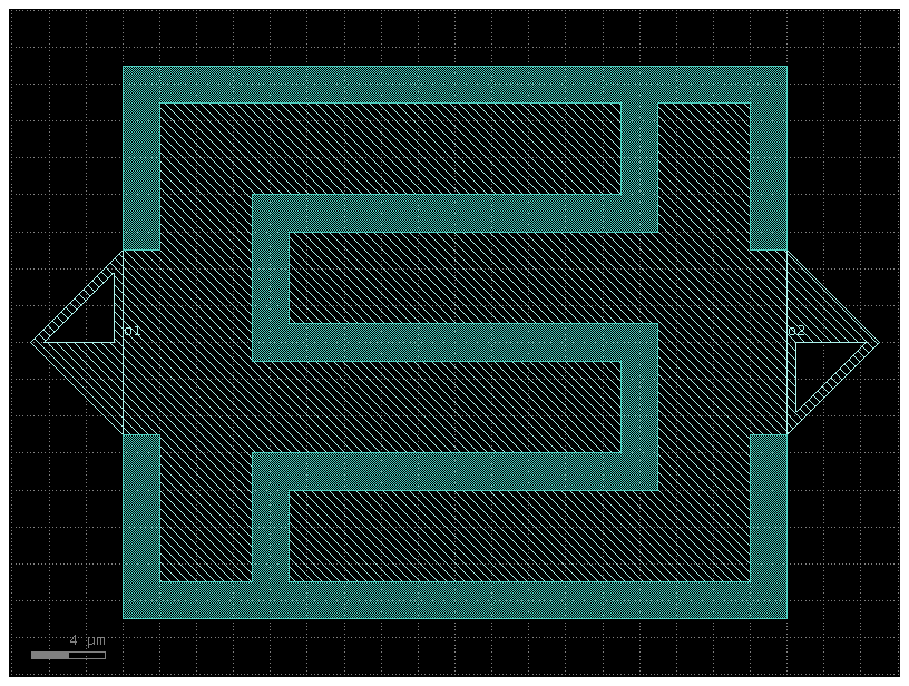
meander_inductor#
- qpdk.cells.meander_inductor(n_turns=5, turn_length=200.0, cross_section=<function meander_inductor_cross_section>, wire_gap=None, etch_bbox_margin=2.0, add_etch=True)[source]#
Creates a meander inductor with Manhattan routing using a narrow wire.
The inductor consists of multiple horizontal runs connected by short vertical segments at alternating ends, forming a serpentine (meander) path. The total inductance is dominated by kinetic inductance for superconducting thin films.

Similar structures are described in [CSD+23, KVH+11].
- Parameters:
n_turns (int) – Number of horizontal meander runs (must be >= 1).
turn_length (float) – Length of each horizontal run in µm.
cross_section (CrossSectionSpec) – Cross-section specification for the meander wire. The center conductor width and etch gap are derived from this specification. The meander’s vertical pitch is set to ensure that the etched regions of adjacent runs do not overlap, maintaining the characteristic impedance of each run. Specifically, the pitch is calculated as \(w + 2g\), where \(w\) is the wire width and \(g\) is the etch gap.
wire_gap (float | None) – Optional explicit gap between adjacent inductor runs in µm. If None (default), it’s inferred as 2x the etch gap from the cross-section.
etch_bbox_margin (float) – Extra margin around the inductor for the etch bounding box in µm. This margin is added in addition to the etch region defined in the cross-section.
add_etch (bool) – Whether to add the etch bounding box. Defaults to True.
- Returns:
- A gdsfactory component with the meander inductor geometry
and two ports (‘o1’ and ‘o2’).
- Return type:
Component
- Raises:
ValueError – If n_turns < 1 or turn_length <= 0.
nxn#
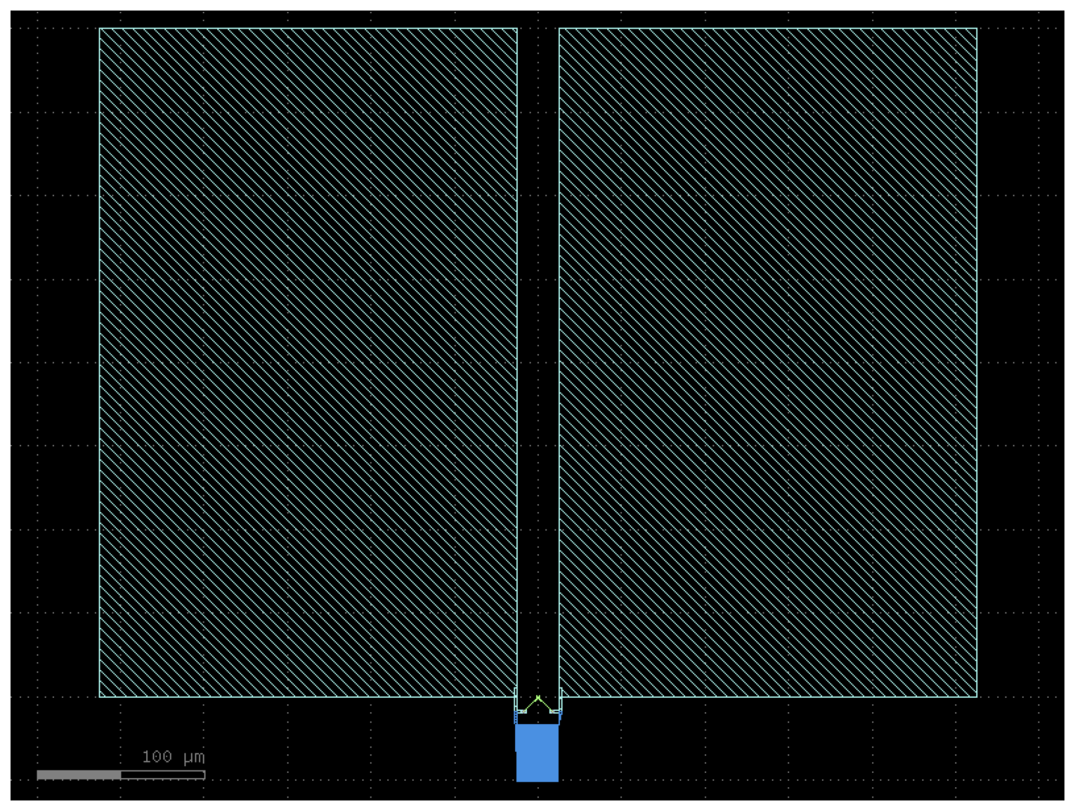
- qpdk.cells.nxn(xsize=10.0, ysize=10.0, wg_width=10.0, layer=<LayerMapQPDK.M1_DRAW: 1>, wg_margin=0.0, north=1, east=1, south=1, west=1, cross_section=<function coplanar_waveguide>)[source]#
Returns an NxN junction with ports on each side.
- Parameters:
xsize (float) – Horizontal size of the junction in μm.
ysize (float) – Vertical size of the junction in μm.
wg_width (float) – Width of the waveguides in μm.
layer (LayerSpec) – Layer specification.
wg_margin (float) – Margin from edge to waveguide in μm.
north (int) – Number of ports on the north side.
east (int) – Number of ports on the east side.
south (int) – Number of ports on the south side.
west (int) – Number of ports on the west side.
cross_section (CrossSectionSpec) – Cross-section specification.
- Return type:
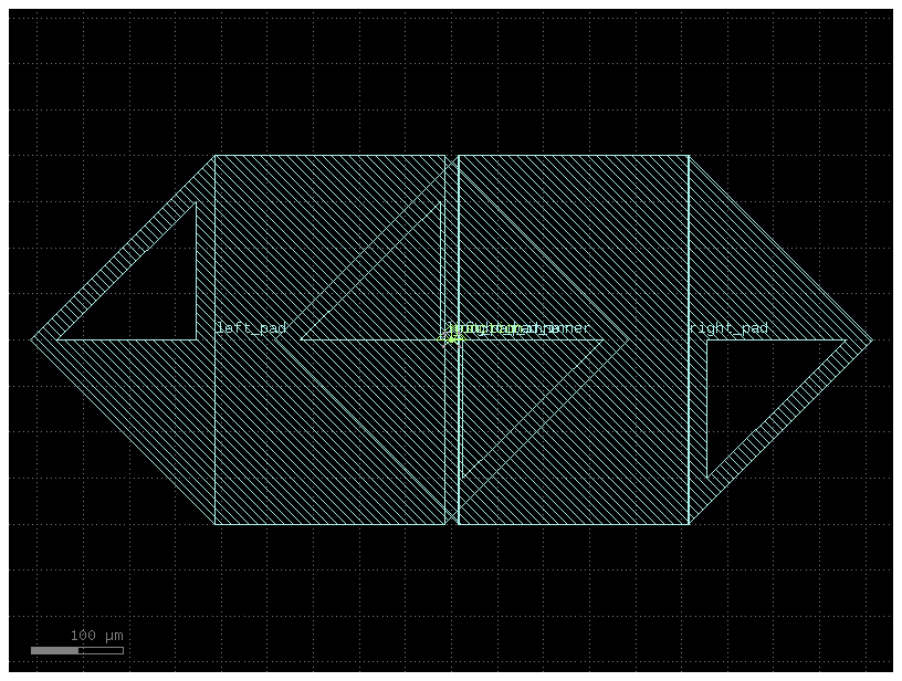
plate_capacitor#
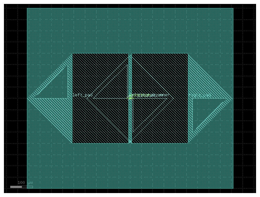
- qpdk.cells.plate_capacitor(length=26.0, width=5.0, gap=7.0, etch_layer='M1_ETCH', etch_bbox_margin=2.0, cross_section='cpw')[source]#
Creates a plate capacitor.
A capacitive coupler consists of two metal pads separated by a small gap, providing capacitive coupling between circuit elements like qubits and resonators.

- Parameters:
length (float) – Length (vertical extent) of the capacitor pad in μm.
width (float) – Width (horizontal extent) of the capacitor pad in μm.
gap (float) – Gap between plates in μm.
etch_layer (TypeAliasForwardRef('LayerSpec') | None) – Optional layer for etching around the capacitor.
etch_bbox_margin (float) – Margin around the capacitor for the etch layer in μm.
cross_section (CrossSectionSpec) – Cross-section for the short straight from the etch box capacitor.
- Returns:
A gdsfactory component with the plate capacitor geometry and two ports (‘o1’ and ‘o2’) on opposing sides.
- Raises:
ValueError – If width or length is not positive.
- Return type:
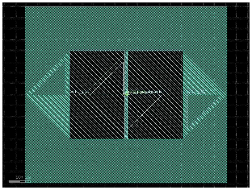
plate_capacitor_single#
- qpdk.cells.plate_capacitor_single(length=26.0, width=5.0, layer_metal=<LayerMapQPDK.M1_DRAW: 1>, etch_layer='M1_ETCH', etch_bbox_margin=2.0, cross_section='cpw')[source]#
Creates a single plate capacitor for coupling.
This is essentially half of a
plate_capacitor().
- Parameters:
length (float) – Length (vertical extent) of the capacitor pad in μm.
width (float) – Width (horizontal extent) of the capacitor pad in μm.
layer_metal (LayerSpec) – Layer for the metal pad.
etch_layer (TypeAliasForwardRef('LayerSpec') | None) – Optional layer for etching around the capacitor.
etch_bbox_margin (float) – Margin around the capacitor for the etch layer in μm.
cross_section (CrossSectionSpec) – Cross-section for the short straight from the etch box capacitor.
- Returns:
A gdsfactory component with the plate capacitor geometry.
- Raises:
ValueError – If width or length is not positive.
- Return type:
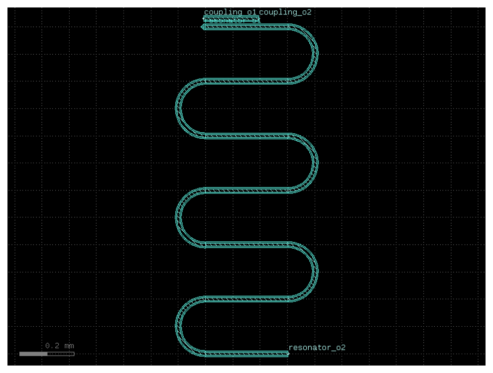
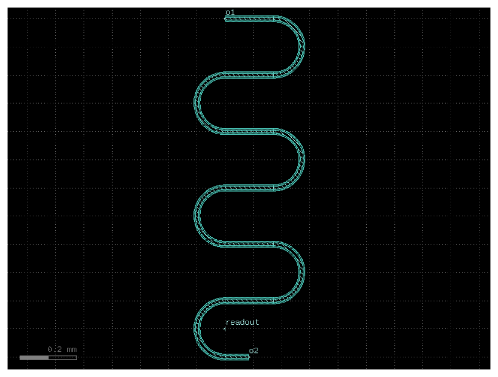
quarter_wave_resonator_coupled#
- qpdk.cells.quarter_wave_resonator_coupled(length=4000.0, meanders=6, bend_spec=<function bend_circular>, cross_section='cpw', *, start_with_bend=False, end_with_bend=False, open_start=True, open_end=False, cross_section_non_resonator='cpw', coupling_straight_length=200.0, coupling_gap=20.0)[source]#
Creates a quarter-wave resonator with a coupling waveguide.
Uses
resonator_coupled()as the basis but removes the shorted end port from the output ports.
- Parameters:
length (float) – Length of the resonator in μm.
meanders (int) – Number of meander sections to fit the resonator in a compact area.
bend_spec (ComponentSpec) – Specification for the bend component used in meanders.
cross_section (CrossSectionSpec) – Cross-section specification for the resonator.
start_with_bend (bool) – If True, starts the resonator with a bend.
end_with_bend (bool) – If True, ends the resonator with a bend.
open_start (bool) – If True, adds an etch section at the start of the resonator.
open_end (bool) – If True, adds an etch section at the end of the resonator.
cross_section_non_resonator (CrossSectionSpec) – Cross-section specification for the coupling waveguide.
coupling_straight_length (float) – Length of the coupling waveguide section in μm.
coupling_gap (float) – Gap between the resonator and coupling waveguide in μm.
- Returns:
The coupled quarter-wave resonator component.
- Return type:
rectangle#
- qpdk.cells.rectangle(size=(4.0, 2.0), layer='M1_DRAW', centered=False, port_type='electrical', port_orientations=(180, 90, 0, -90))[source]#
Returns a rectangle.
- Parameters:
size (Size) – (tuple) Width and height of rectangle.
layer (LayerSpec) – Specific layer to put polygon geometry on.
centered (bool) – True sets center to (0.0, 0.0), False sets south-west to (0.0, 0.0).
port_type (str | None) – optical, electrical.
port_orientations (Ints | None) – list of port_orientations to add. None adds no ports.
- Return type:
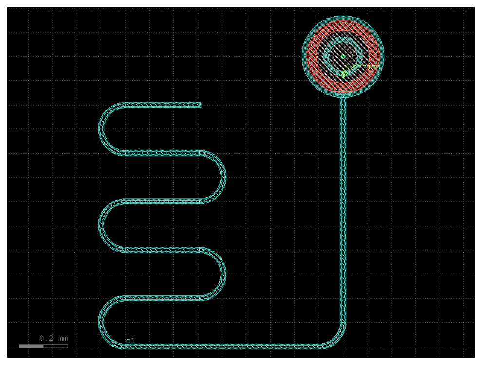
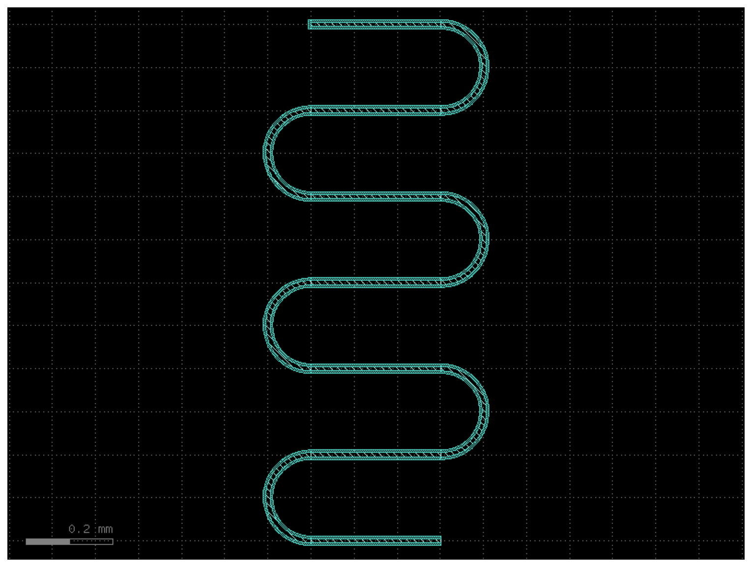
resonator#
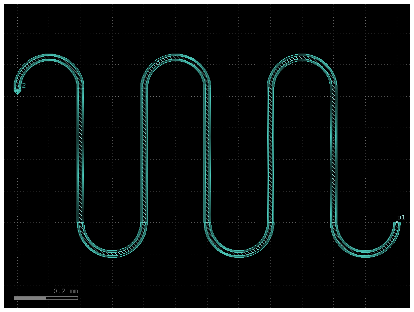
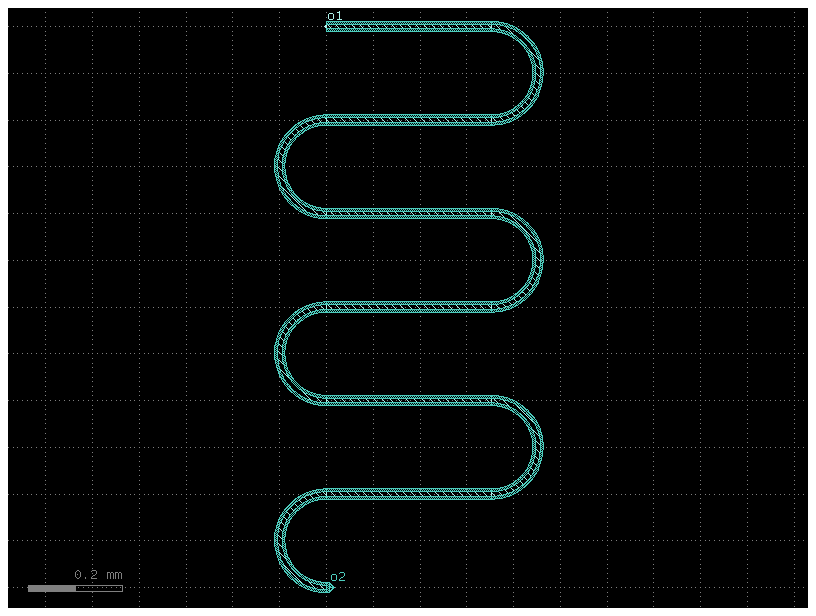
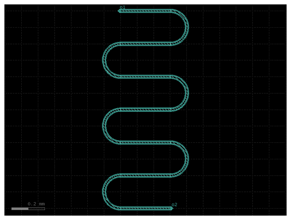
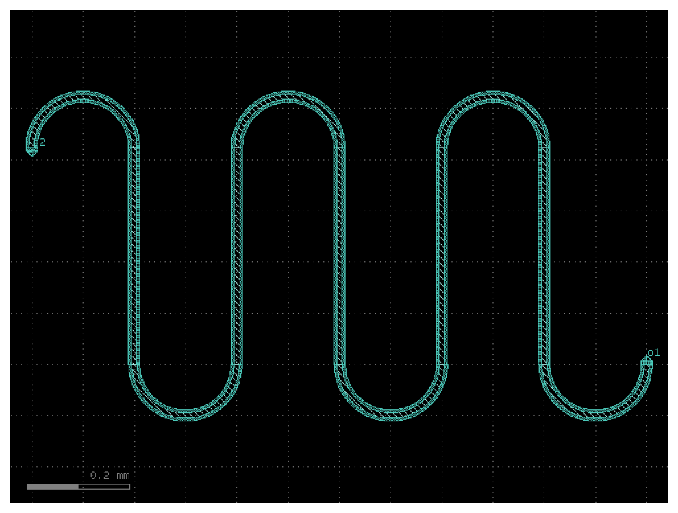
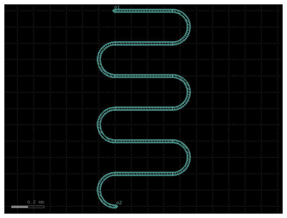
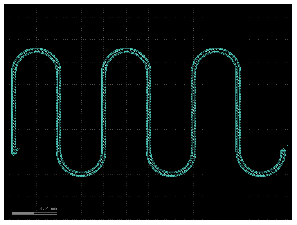
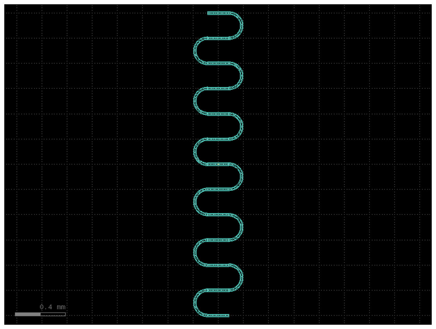
- qpdk.cells.resonator(length=4000.0, meanders=6, bend_spec=<function bend_circular>, cross_section='cpw', *, start_with_bend=False, end_with_bend=False, open_start=True, open_end=False)[source]#
Creates a meandering coplanar waveguide resonator.
Changing open_start and open_end appropriately allows creating a shorted quarter-wave resonator or an open half-wave resonator.

See [MP12] for details
- Parameters:
length (float) – Length of the resonator in μm.
meanders (int) – Number of meander sections to fit the resonator in a compact area.
bend_spec (ComponentSpec) – Specification for the bend component used in meanders.
cross_section (CrossSectionSpec) – Cross-section specification for the resonator.
start_with_bend (bool) – If True, starts the resonator with a bend.
end_with_bend (bool) – If True, ends the resonator with a bend.
open_start (bool) – If True, adds an etch section at the start of the resonator.
open_end (bool) – If True, adds an etch section at the end of the resonator.
- Returns:
A gdsfactory component with meandering resonator geometry.
- Return type:
Component
- Raises:
ValueError – If length is too short for the requested meanders.
resonator_coupled#
- qpdk.cells.resonator_coupled(length=4000.0, meanders=6, bend_spec=<function bend_circular>, cross_section='cpw', *, start_with_bend=False, end_with_bend=False, open_start=True, open_end=False, cross_section_non_resonator='cpw', coupling_straight_length=200.0, coupling_gap=20.0)[source]#
Creates a meandering coplanar waveguide resonator with a coupling waveguide.
This component combines a resonator with a parallel coupling waveguide placed at a specified gap for proximity coupling. Similar to the design described in [BM18].

- Parameters:
length (float) – Length of the resonator in μm.
meanders (int) – Number of meander sections to fit the resonator in a compact area.
bend_spec (ComponentSpec) – Specification for the bend component used in meanders.
cross_section (CrossSectionSpec) – Cross-section specification for the resonator.
start_with_bend (bool) – If True, starts the resonator with a bend.
end_with_bend (bool) – If True, ends the resonator with a bend.
open_start (bool) – If True, adds an etch section at the start of the resonator.
open_end (bool) – If True, adds an etch section at the end of the resonator.
cross_section_non_resonator (CrossSectionSpec) – Cross-section specification for the coupling waveguide.
coupling_straight_length (float) – Length of the coupling waveguide section in μm.
coupling_gap (float) – Gap between the resonator and coupling waveguide in μm. Measured from edges of the center conductors.
- Returns:
A gdsfactory component with meandering resonator and coupling waveguide.
- Return type:
Component
resonator_half_wave#
- qpdk.cells.resonator_half_wave(length=4000.0, meanders=6, bend_spec=<function bend_circular>, cross_section='cpw', *, start_with_bend=False, end_with_bend=False, open_start=True, open_end=True)#
Creates a meandering coplanar waveguide resonator.
Changing open_start and open_end appropriately allows creating a shorted quarter-wave resonator or an open half-wave resonator.
See [MP12] for details
- Parameters:
length (float) – Length of the resonator in μm.
meanders (int) – Number of meander sections to fit the resonator in a compact area.
bend_spec (ComponentSpec) – Specification for the bend component used in meanders.
cross_section (CrossSectionSpec) – Cross-section specification for the resonator.
start_with_bend (bool) – If True, starts the resonator with a bend.
end_with_bend (bool) – If True, ends the resonator with a bend.
open_start (bool) – If True, adds an etch section at the start of the resonator.
open_end (bool) – If True, adds an etch section at the end of the resonator.
- Returns:
A gdsfactory component with meandering resonator geometry.
- Return type:
Component
- Raises:
ValueError – If length is too short for the requested meanders.
resonator_half_wave_bend_both#
- qpdk.cells.resonator_half_wave_bend_both(length=4000.0, meanders=6, bend_spec=<function bend_circular>, cross_section='cpw', *, start_with_bend=True, end_with_bend=True, open_start=True, open_end=True)#
Creates a meandering coplanar waveguide resonator.
Changing open_start and open_end appropriately allows creating a shorted quarter-wave resonator or an open half-wave resonator.
See [MP12] for details
- Parameters:
length (float) – Length of the resonator in μm.
meanders (int) – Number of meander sections to fit the resonator in a compact area.
bend_spec (ComponentSpec) – Specification for the bend component used in meanders.
cross_section (CrossSectionSpec) – Cross-section specification for the resonator.
start_with_bend (bool) – If True, starts the resonator with a bend.
end_with_bend (bool) – If True, ends the resonator with a bend.
open_start (bool) – If True, adds an etch section at the start of the resonator.
open_end (bool) – If True, adds an etch section at the end of the resonator.
- Returns:
A gdsfactory component with meandering resonator geometry.
- Return type:
Component
- Raises:
ValueError – If length is too short for the requested meanders.
resonator_half_wave_bend_end#
- qpdk.cells.resonator_half_wave_bend_end(length=4000.0, meanders=6, bend_spec=<function bend_circular>, cross_section='cpw', *, start_with_bend=False, end_with_bend=True, open_start=True, open_end=True)#
Creates a meandering coplanar waveguide resonator.
Changing open_start and open_end appropriately allows creating a shorted quarter-wave resonator or an open half-wave resonator.
See [MP12] for details
- Parameters:
length (float) – Length of the resonator in μm.
meanders (int) – Number of meander sections to fit the resonator in a compact area.
bend_spec (ComponentSpec) – Specification for the bend component used in meanders.
cross_section (CrossSectionSpec) – Cross-section specification for the resonator.
start_with_bend (bool) – If True, starts the resonator with a bend.
end_with_bend (bool) – If True, ends the resonator with a bend.
open_start (bool) – If True, adds an etch section at the start of the resonator.
open_end (bool) – If True, adds an etch section at the end of the resonator.
- Returns:
A gdsfactory component with meandering resonator geometry.
- Return type:
Component
- Raises:
ValueError – If length is too short for the requested meanders.
resonator_half_wave_bend_start#
- qpdk.cells.resonator_half_wave_bend_start(length=4000.0, meanders=6, bend_spec=<function bend_circular>, cross_section='cpw', *, start_with_bend=True, end_with_bend=False, open_start=True, open_end=True)#
Creates a meandering coplanar waveguide resonator.
Changing open_start and open_end appropriately allows creating a shorted quarter-wave resonator or an open half-wave resonator.
See [MP12] for details
- Parameters:
length (float) – Length of the resonator in μm.
meanders (int) – Number of meander sections to fit the resonator in a compact area.
bend_spec (ComponentSpec) – Specification for the bend component used in meanders.
cross_section (CrossSectionSpec) – Cross-section specification for the resonator.
start_with_bend (bool) – If True, starts the resonator with a bend.
end_with_bend (bool) – If True, ends the resonator with a bend.
open_start (bool) – If True, adds an etch section at the start of the resonator.
open_end (bool) – If True, adds an etch section at the end of the resonator.
- Returns:
A gdsfactory component with meandering resonator geometry.
- Return type:
Component
- Raises:
ValueError – If length is too short for the requested meanders.
resonator_quarter_wave#
- qpdk.cells.resonator_quarter_wave(length=4000.0, meanders=6, bend_spec=<function bend_circular>, cross_section='cpw', *, start_with_bend=False, end_with_bend=False, open_start=False, open_end=True)#
Creates a meandering coplanar waveguide resonator.
Changing open_start and open_end appropriately allows creating a shorted quarter-wave resonator or an open half-wave resonator.
See [MP12] for details
- Parameters:
length (float) – Length of the resonator in μm.
meanders (int) – Number of meander sections to fit the resonator in a compact area.
bend_spec (ComponentSpec) – Specification for the bend component used in meanders.
cross_section (CrossSectionSpec) – Cross-section specification for the resonator.
start_with_bend (bool) – If True, starts the resonator with a bend.
end_with_bend (bool) – If True, ends the resonator with a bend.
open_start (bool) – If True, adds an etch section at the start of the resonator.
open_end (bool) – If True, adds an etch section at the end of the resonator.
- Returns:
A gdsfactory component with meandering resonator geometry.
- Return type:
Component
- Raises:
ValueError – If length is too short for the requested meanders.
resonator_quarter_wave_bend_both#
- qpdk.cells.resonator_quarter_wave_bend_both(length=4000.0, meanders=6, bend_spec=<function bend_circular>, cross_section='cpw', *, start_with_bend=True, end_with_bend=True, open_start=False, open_end=True)#
Creates a meandering coplanar waveguide resonator.
Changing open_start and open_end appropriately allows creating a shorted quarter-wave resonator or an open half-wave resonator.
See [MP12] for details
- Parameters:
length (float) – Length of the resonator in μm.
meanders (int) – Number of meander sections to fit the resonator in a compact area.
bend_spec (ComponentSpec) – Specification for the bend component used in meanders.
cross_section (CrossSectionSpec) – Cross-section specification for the resonator.
start_with_bend (bool) – If True, starts the resonator with a bend.
end_with_bend (bool) – If True, ends the resonator with a bend.
open_start (bool) – If True, adds an etch section at the start of the resonator.
open_end (bool) – If True, adds an etch section at the end of the resonator.
- Returns:
A gdsfactory component with meandering resonator geometry.
- Return type:
Component
- Raises:
ValueError – If length is too short for the requested meanders.
resonator_quarter_wave_bend_end#
- qpdk.cells.resonator_quarter_wave_bend_end(length=4000.0, meanders=6, bend_spec=<function bend_circular>, cross_section='cpw', *, start_with_bend=False, end_with_bend=True, open_start=False, open_end=True)#
Creates a meandering coplanar waveguide resonator.
Changing open_start and open_end appropriately allows creating a shorted quarter-wave resonator or an open half-wave resonator.
See [MP12] for details
- Parameters:
length (float) – Length of the resonator in μm.
meanders (int) – Number of meander sections to fit the resonator in a compact area.
bend_spec (ComponentSpec) – Specification for the bend component used in meanders.
cross_section (CrossSectionSpec) – Cross-section specification for the resonator.
start_with_bend (bool) – If True, starts the resonator with a bend.
end_with_bend (bool) – If True, ends the resonator with a bend.
open_start (bool) – If True, adds an etch section at the start of the resonator.
open_end (bool) – If True, adds an etch section at the end of the resonator.
- Returns:
A gdsfactory component with meandering resonator geometry.
- Return type:
Component
- Raises:
ValueError – If length is too short for the requested meanders.
resonator_quarter_wave_bend_start#
- qpdk.cells.resonator_quarter_wave_bend_start(length=4000.0, meanders=6, bend_spec=<function bend_circular>, cross_section='cpw', *, start_with_bend=True, end_with_bend=False, open_start=False, open_end=True)#
Creates a meandering coplanar waveguide resonator.
Changing open_start and open_end appropriately allows creating a shorted quarter-wave resonator or an open half-wave resonator.
See [MP12] for details
- Parameters:
length (float) – Length of the resonator in μm.
meanders (int) – Number of meander sections to fit the resonator in a compact area.
bend_spec (ComponentSpec) – Specification for the bend component used in meanders.
cross_section (CrossSectionSpec) – Cross-section specification for the resonator.
start_with_bend (bool) – If True, starts the resonator with a bend.
end_with_bend (bool) – If True, ends the resonator with a bend.
open_start (bool) – If True, adds an etch section at the start of the resonator.
open_end (bool) – If True, adds an etch section at the end of the resonator.
- Returns:
A gdsfactory component with meandering resonator geometry.
- Return type:
Component
- Raises:
ValueError – If length is too short for the requested meanders.

ring#
- qpdk.cells.ring(radius=10.0, width=0.5, angle_resolution=2.5, layer='WG', angle=360, distance_resolution=None)[source]#
Returns a ring.
- Parameters:
radius (float) – ring radius.
width (float) – of the ring.
angle_resolution (float) – max number of degrees per point.
layer (LayerSpec) – layer.
angle (float) – angular coverage of the ring
distance_resolution (float | None) – max distance between points. This is an alternate way to describe the resolution besides setting angle_resolution. If distance_resolution and angle_resolution are both set, distance_resolution determines the resolution.
- Return type:
single_josephson_junction_wire#
- qpdk.cells.single_josephson_junction_wire(wide_straight_length=8.3, narrow_straight_length=0.5, taper_length=4.7, cross_section_wide=<function josephson_junction_cross_section_wide>, cross_section_narrow=<function josephson_junction_cross_section_narrow>, layer_patch=<LayerMapQPDK.JJ_PATCH: 51>, size_patch=(1.5, 1.0))[source]#
Creates a single wire to use in a Josephson junction.

- Parameters:
wide_straight_length (float) – Length of the wide straight section in µm.
narrow_straight_length (float) – Length of the narrow straight section in µm.
taper_length (float) – Length of the taper section in µm.
cross_section_wide (CrossSectionSpec) – Cross-section specification for the wide section.
cross_section_narrow (CrossSectionSpec) – Cross-section specification for the narrow section.
layer_patch (LayerSpec) – Layer for the patch that creates the overlap region.
size_patch (tuple[float, float]) – Size of the patch that creates the overlap region.
- Returns:
The junction wire component.
- Return type:
snspd#
- qpdk.cells.snspd(wire_width=0.2, wire_pitch=0.6, size=(10, 8), num_squares=None, turn_ratio=4, terminals_same_side=False, layer=<LayerMapQPDK.NbTiN: 18>, port_type='electrical')[source]#
Creates an optimally-rounded SNSPD.

- Parameters:
wire_width (float) – Width of the wire.
wire_pitch (float) – Distance between two adjacent wires. Must be greater than width.
size (Size) – Float2 (width, height) of the rectangle formed by the outer boundary of the SNSPD.
num_squares (int | None) – int | None = None Total number of squares inside the SNSPD length.
turn_ratio (float) – float Specifies how much of the SNSPD width is dedicated to the 180 degree turn. A turn_ratio of 10 will result in 20% of the width being comprised of the turn.
terminals_same_side (bool) – If True, both ports will be located on the same side of the SNSPD.
layer (LayerSpec) – layer spec to put polygon geometry on.
port_type (str) – type of port to add to the component.
- Returns:
A Component containing the SNSPD geometry.
- Return type:
squid_junction#
- qpdk.cells.squid_junction(junction_spec=<function josephson_junction>, loop_area=4)[source]#
Creates a SQUID (Superconducting Quantum Interference Device) junction component.
A SQUID consists of two Josephson junctions connected in parallel, forming a loop.
See [CB04] for details.
squid_junction_long#
- qpdk.cells.squid_junction_long(**kwargs)[source]#
SQUID junction with josephson_junction_long.
- Returns:
The SQUID junction component with long wires.
- Return type:
straight#
- qpdk.cells.straight(length=10.0, cross_section=<function coplanar_waveguide>, width=None, npoints=2)[source]#
Returns a straight waveguide.

straight_all_angle#
- qpdk.cells.straight_all_angle(length=10.0, npoints=2, cross_section=<function coplanar_waveguide>, width=None)[source]#
Returns a Straight waveguide with offgrid ports.
- Parameters:
- Return type:
o1  ──────────────── o2
        length
straight_double_open#
- qpdk.cells.straight_double_open(length=10.0, cross_section=<function coplanar_waveguide>, width=None, npoints=2)[source]#
Returns a straight waveguide with etched gaps at both ends.
Note
This may be treated as a \(\lambda/2\) straight resonator in some contexts.
straight_open#
- qpdk.cells.straight_open(length=10.0, cross_section=<function coplanar_waveguide>, width=None, npoints=2)[source]#
Returns a straight waveguide with etched gap at one end.
straight_shorted#
- qpdk.cells.straight_shorted(length=10.0, cross_section=<function coplanar_waveguide>, width=None, npoints=2)#
Returns a straight waveguide.
taper_cross_section#
- qpdk.cells.taper_cross_section(*, cross_section1='cpw', cross_section2='cpw', length=10, npoints=100, linear=False, width_type='sine', exclude_layers=None)#
Returns taper transition between cross_section1 and cross_section2.
- Parameters:
cross_section1 (CrossSectionSpec) – start cross_section factory.
cross_section2 (CrossSectionSpec) – end cross_section factory.
length (float) – transition length.
npoints (int) – number of points.
linear (bool) – shape of the transition, sine when False.
width_type (str) – shape of the transition ONLY IF linear is False
exclude_layers (LayerSpecs | None) – layers to exclude from the transition. Sections on these layers will be omitted from the component.
- Return type:
Component

tee#
- qpdk.cells.tee(cross_section='cpw')[source]#
Returns a three-way tee waveguide.
- Parameters:
cross_section (CrossSectionSpec) – specification (CrossSection, string or dict).
- Return type:
transform_component#
transmon_with_resonator#
- qpdk.cells.transmon_with_resonator(qubit='double_pad_transmon_with_bbox', resonator=functools.partial(<function resonator>, open_start=False, open_end=True, start_with_bend=True, length=4000, meanders=6), resonator_meander_start=(-900, -1200), resonator_length=5000.0, resonator_meanders=5, resonator_bend_spec='bend_circular', resonator_cross_section='cpw', resonator_open_start=False, resonator_open_end=True, coupler=functools.partial(<function plate_capacitor_single>, width=20, length=394), qubit_rotation=90, coupler_port='left_pad', coupler_offset=(-45, 0))[source]#
Returns a transmon qubit coupled to a quarter wave resonator.
- Parameters:
qubit (ComponentSpec) – Qubit component.
resonator (ComponentSpec) – Resonator component.
resonator_meander_start (tuple[float, float]) – (x, y) position of the start of the resonator meander.
resonator_length (float) – Length of the resonator in µm.
resonator_meanders (int) – Number of meander sections for the resonator.
resonator_bend_spec (ComponentSpec) – Specification for the bend component used in meanders.
resonator_cross_section (CrossSectionSpec) – Cross-section specification for the resonator.
resonator_open_start (bool) – If True, adds an etch section at the start of the resonator.
resonator_open_end (bool) – If True, adds an etch section at the end of the resonator.
coupler (ComponentSpec) – Coupler spec.
qubit_rotation (float) – Rotation angle for the qubit in degrees.
coupler_port (str) – Name of the qubit port to position the coupler relative to.
coupler_offset (tuple[float, float]) – (x, y) offset for the coupler position.
- Return type:
transmon_with_resonator_and_probeline#
- qpdk.cells.transmon_with_resonator_and_probeline(qubit='double_pad_transmon_with_bbox', resonator=functools.partial(<function resonator>, open_start=False, open_end=True, start_with_bend=True, length=4000, meanders=6), resonator_meander_start=(-900, -1200), resonator_length=5000.0, resonator_meanders=5, resonator_bend_spec='bend_circular', resonator_cross_section='cpw', resonator_open_start=False, resonator_open_end=True, coupler=functools.partial(<function plate_capacitor_single>, width=20, length=394), qubit_rotation=90, coupler_port='left_pad', coupler_offset=(-45, 0), probeline_coupler=functools.partial(<function coupler_straight>, cross_section='cpw', gap=16), probeline_coupling_gap=16.0, probeline_coupling_length=None)[source]#
Returns a transmon qubit coupled to a quarter wave resonator and a probeline.
Uses a
coupler_straight()to couple the resonator to a probeline. The coupling section is inserted at the start of the resonator meander, with one waveguide carrying the resonator signal and the other providing ports for probeline routing.- Parameters:
qubit (ComponentSpec) – Qubit component.
resonator (ComponentSpec) – Resonator component.
resonator_meander_start (tuple[float, float]) – (x, y) position of the start of the resonator meander.
resonator_length (float) – Length of the resonator in µm.
resonator_meanders (int) – Number of meander sections for the resonator.
resonator_bend_spec (ComponentSpec) – Specification for the bend component used in meanders.
resonator_cross_section (CrossSectionSpec) – Cross-section specification for the resonator.
resonator_open_start (bool) – If True, adds an etch section at the start of the resonator.
resonator_open_end (bool) – If True, adds an etch section at the end of the resonator.
coupler (ComponentSpec) – Coupler spec.
qubit_rotation (float) – Rotation angle for the qubit in degrees.
coupler_port (str) – Name of the qubit port to position the coupler relative to.
coupler_offset (tuple[float, float]) – (x, y) offset for the coupler position.
probeline_coupler (ComponentSpec) – Component spec for the probeline coupling section.
probeline_coupling_gap (float) – Gap between the resonator and probeline waveguides in the coupling section in µm.
probeline_coupling_length (float | None) – Length of the coupling section in µm.
- Return type:
tsv#
- qpdk.cells.tsv(diameter=15.0)[source]#
Creates a Through-silicon via (TSV) component for 3D integration.
See [YSM+20].
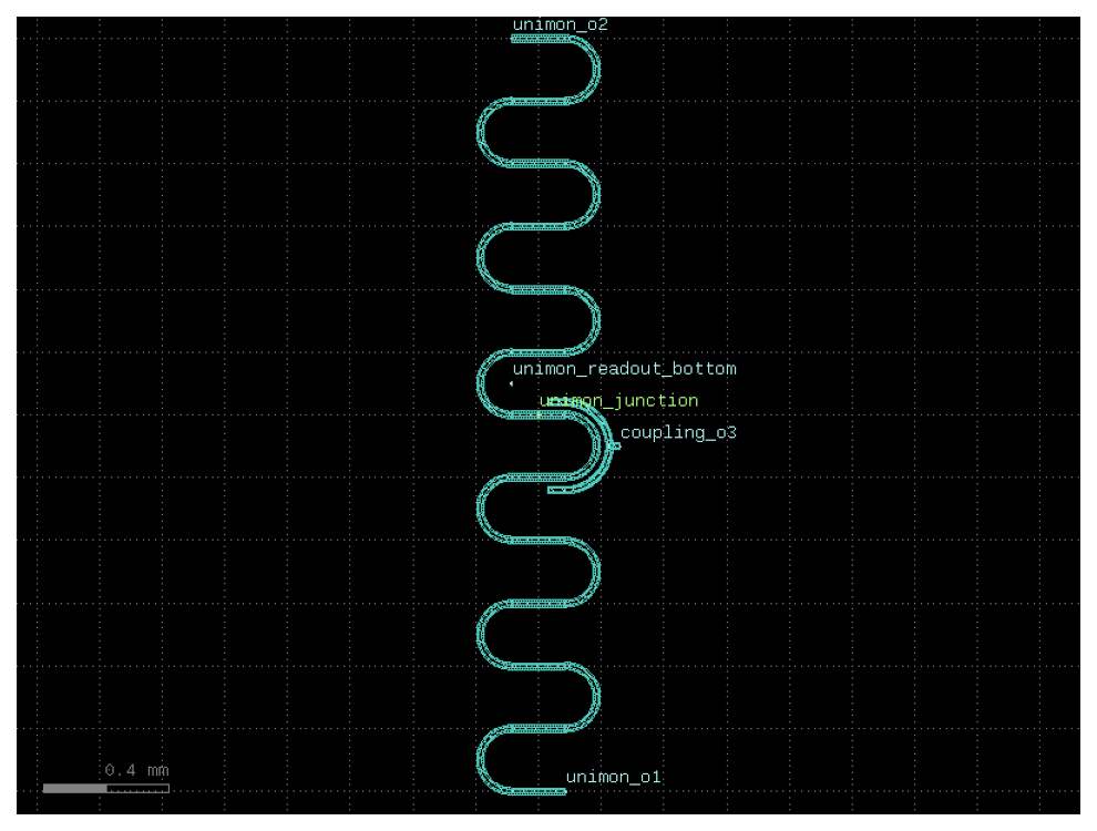
unimon#
- qpdk.cells.unimon(arm_length=3000.0, arm_meanders=6, bend_spec=<function bend_circular>, cross_section='cpw', junction_spec=functools.partial(<function squid_junction>, junction_spec=functools.partial(<function josephson_junction>, junction_overlap_displacement=1.8, wide_straight_length=4.0, narrow_straight_length=0.5, taper_length=4)), junction_gap=10.0, junction_etch_width=22.0)[source]#
Creates a unimon qubit from two grounded \(\lambda/4\) CPW resonator arms connected by a SQUID junction.
The unimon is a superconducting qubit consisting of a single Josephson junction (or SQUID for flux tunability) embedded in the center of a two grounded \(\lambda/4\) CPW resonators, providing a large geometric inductance that, together with the Josephson nonlinearity, yields high anharmonicity and resilience to charge noise.

See [HKC+22, TVT+24] for details.
- Parameters:
arm_length (float) – Length of each \(\lambda/4\) resonator arm in µm.
arm_meanders (int) – Number of meander sections in each arm.
bend_spec (ComponentSpec) – Specification for the bend component used in meanders.
cross_section (CrossSectionSpec) – Cross-section specification for the resonator arms.
junction_spec (ComponentSpec) – Component specification for the junction (SQUID) component.
junction_gap (float) – Length of the etched gap on which the junction sits in µm.
junction_etch_width (float) – Width of the etched region where the junction sits in µm.
- Returns:
A gdsfactory component with the unimon qubit geometry.
- Return type:
Component
unimon_arm#
- qpdk.cells.unimon_arm(arm_length=3000.0, arm_meanders=6, bend_spec=<function bend_circular>, cross_section='cpw', junction_gap=6.0)[source]#
Creates a quarter-wave resonator arm for the unimon qubit.
- Parameters:
arm_length (float) – Length of the resonator arm in µm.
arm_meanders (int) – Number of meanders in the arm.
bend_spec (ComponentSpec) – Specification for the bend component.
cross_section (CrossSectionSpec) – Cross-section specification for the arm.
junction_gap (float) – Gap for the junction in µm.
- Returns:
The quarter-wave resonator arm component.
- Return type:
Component
unimon_coupled#
- qpdk.cells.unimon_coupled(arm_length=3000.0, arm_meanders=6, bend_spec=<function bend_circular>, cross_section='cpw', junction_spec=functools.partial(<function squid_junction>, junction_spec=functools.partial(<function josephson_junction>, junction_overlap_displacement=1.8, wide_straight_length=4.0, narrow_straight_length=0.5, taper_length=4)), junction_gap=6.0, junction_etch_width=22.0, coupling_gap=30.0, coupling_angle=180.0, coupling_extension_length=50.0, cross_section_non_resonator='cpw')[source]#
Creates a unimon qubit with a half-circle coupling waveguide for readout.
This component combines a
unimon()qubit with a half-circle coupler placed at a specified gap for proximity coupling to a readout resonator.
- Parameters:
arm_length (float) – Length of each \(\lambda/4\) resonator arm in µm.
arm_meanders (int) – Number of meander sections in each arm.
bend_spec (ComponentSpec) – Specification for the bend component used in meanders.
cross_section (CrossSectionSpec) – Cross-section specification for the resonator arms.
junction_spec (ComponentSpec) – Component specification for the junction (SQUID) component.
junction_gap (float) – Length of the etched gap on which the junction sits in µm.
junction_etch_width (float) – Width of the etched region where the junction sits in µm.
coupling_gap (float) – Edge-to-edge gap between M1_DRAW centre conductors of the unimon resonator and the coupling waveguide in µm. The coupling radius is automatically computed as
meander_radius + coupling_gap + width_resonator/2 + width_coupler/2to ensure a uniform gap across the bend.coupling_angle (float) – Angle of the circular arc in degrees.
coupling_extension_length (float) – Length of the straight sections extending from the ends of the half-circle in μm.
cross_section_non_resonator (CrossSectionSpec) – Cross-section for the coupling waveguide.
- Returns:
A gdsfactory component with the unimon and half-circle coupler.
- Return type:
Component
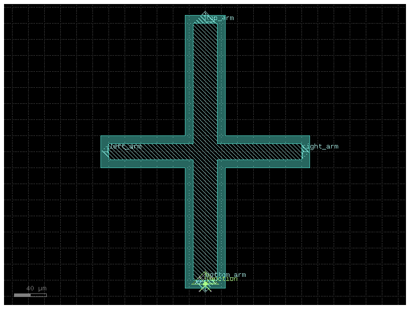
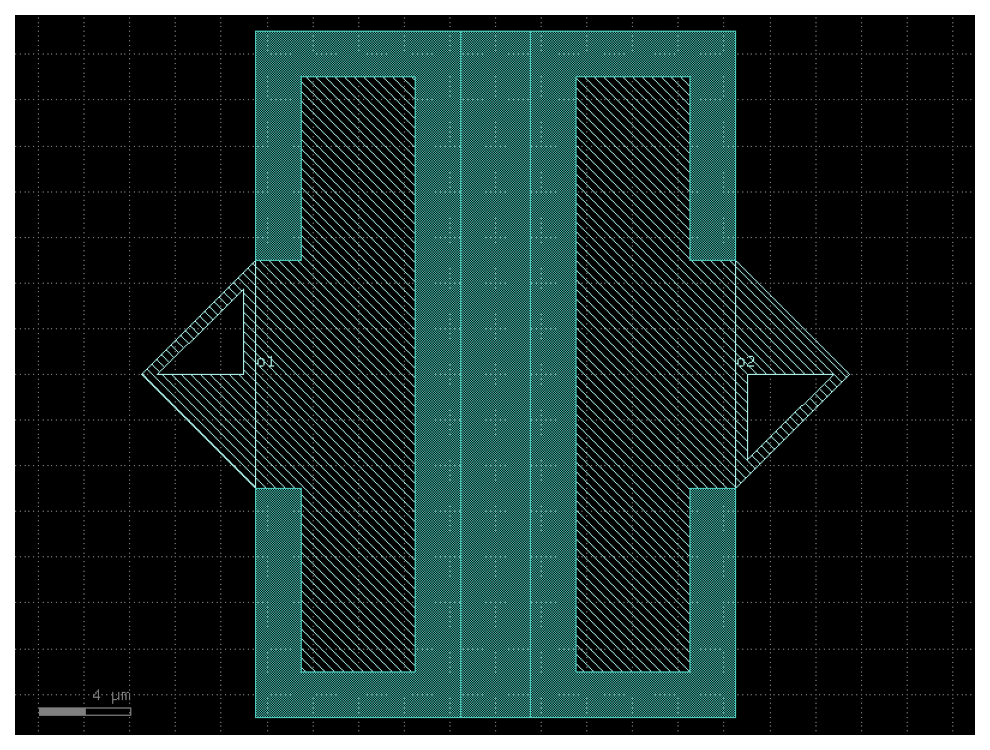
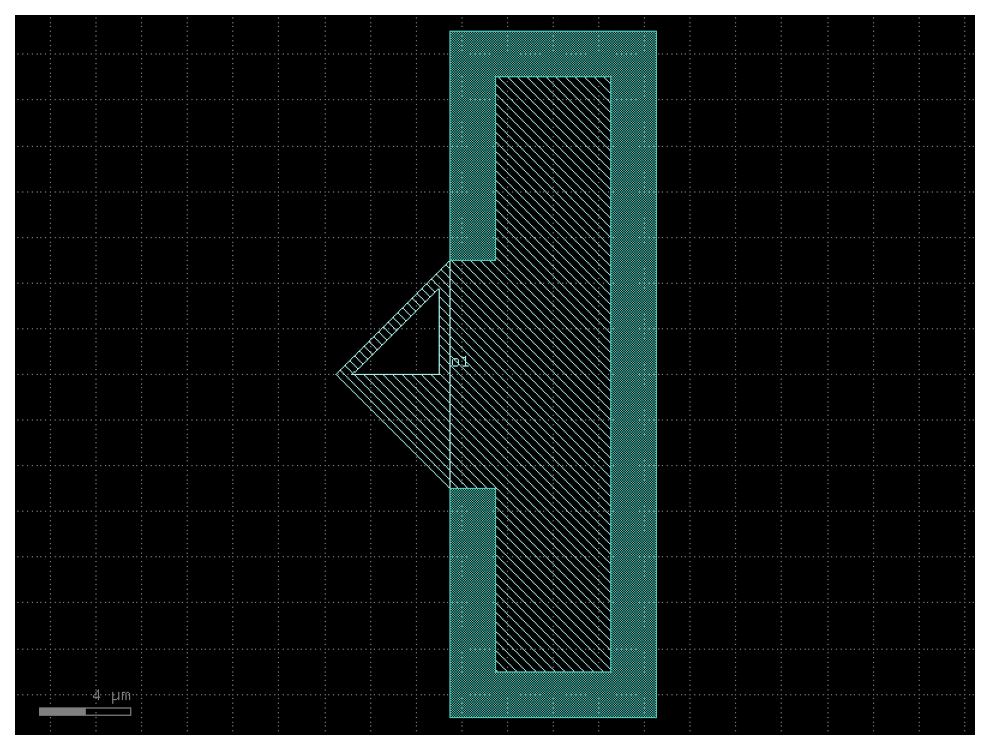
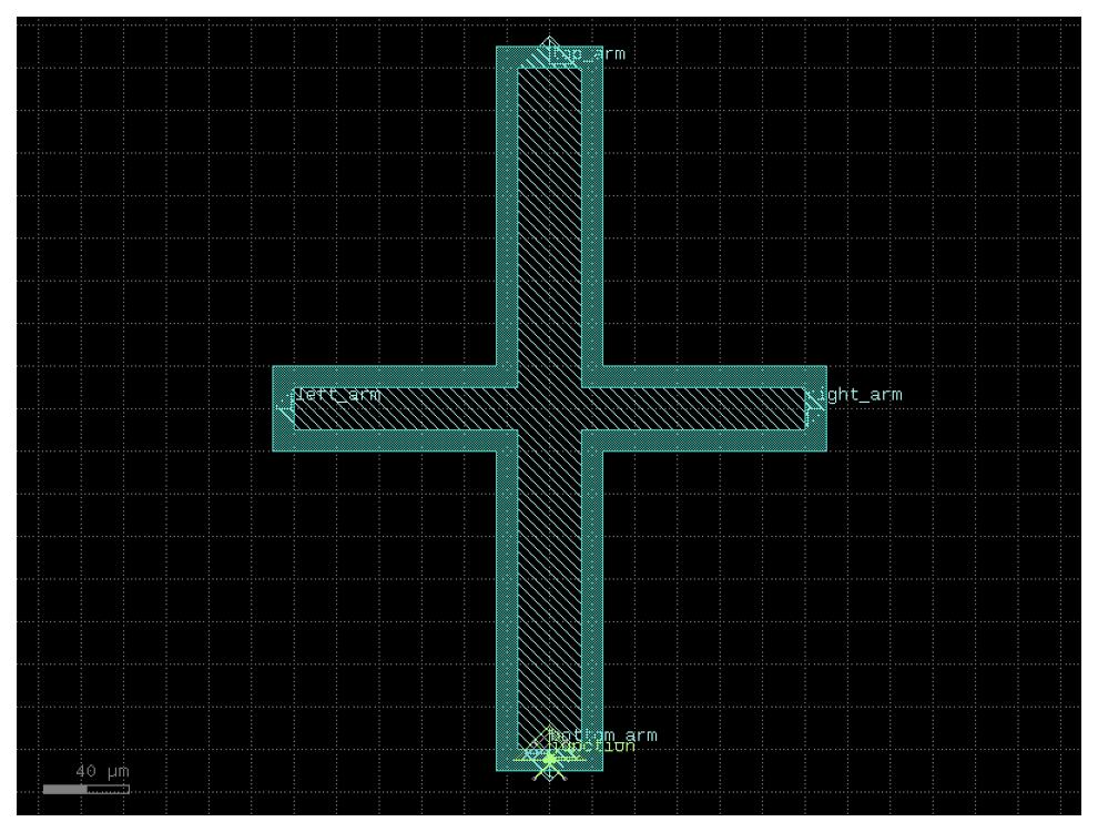
xmon_transmon#
- qpdk.cells.xmon_transmon(arm_width=(30.0, 20.0, 30.0, 20.0), arm_lengths=(160.0, 120.0, 160.0, 120.0), gap_width=10.0, junction_spec=<function squid_junction>, junction_displacement=None, layer_metal=<LayerMapQPDK.M1_DRAW: 1>, layer_etch=<LayerMapQPDK.M1_ETCH: 47>)[source]#
Creates an Xmon style transmon qubit with cross-shaped geometry.
An Xmon transmon consists of a cross-shaped capacitor pad with four arms extending from a central region, connected by a Josephson junction at the center. The design provides better control over the coupling to readout resonators and neighboring qubits through the individual arm geometries.

See [BKM+13] for details about the Xmon design.
- Parameters:
arm_width (tuple[float, float, float, float]) – Tuple of (top, right, bottom, left) arm widths in μm.
arm_lengths (tuple[float, float, float, float]) – Tuple of (top, right, bottom, left) arm lengths in μm. Computed from center to end of each arm.
gap_width (float) – Width of the etched gap around arms in μm.
junction_spec (ComponentSpec) – Component specification for the Josephson junction component.
junction_displacement (DCplxTrans | None) – Optional complex transformation to apply to the junction.
layer_metal (LayerSpec) – Layer for the metal pads.
layer_etch (LayerSpec) – Layer for the etched regions.
- Returns:
A gdsfactory component with the Xmon transmon geometry.
- Return type:
Component
References#
R. Barends, J. Kelly, A. Megrant, D. Sank, E. Jeffrey, Y. Chen, Y. Yin, B. Chiaro, J. Mutus, C. Neill, P. O'Malley, P. Roushan, J. Wenner, T. C. White, A. N. Cleland, and John M. Martinis. Coherent Josephson Qubit Suitable for Scalable Quantum Integrated Circuits. Physical Review Letters, 111(8):080502, August 2013. doi:10.1103/PhysRevLett.111.080502.
Ilya Besedin and Alexey P Menushenkov. Quality factor of a transmission line coupled coplanar waveguide resonator. EPJ Quantum Technology, 5(1):2, December 2018. doi:10.1140/epjqt/s40507-018-0066-3.
Qi-Ming Chen, Priyank Singh, Rostislav Duda, Giacomo Catto, Aarne Keränen, Arman Alizadeh, Timm Mörstedt, Aashish Sah, András Gunyhó, Wei Liu, and Mikko Möttönen. Compact inductor-capacitor resonators at sub-gigahertz frequencies. Physical Review Research, 5(4):043126, November 2023. doi:10.1103/PhysRevResearch.5.043126.
John Clarke and Alex I. Braginski. The SQUID Handbook. Wiley-VCH, Weinheim, 2004. ISBN 978-3-527-40229-8.
Eric Hyyppa, Suman Kundu, Chun Fai Chan, András Gunyhó, Juho Hotari, David Janzso, Kristinn Juliusson, Olavi Kiuru, Janne Kotilahti, Alessandro Landra, Wei Liu, Fabian Marxer, Akseli Mäkinen, Jean-Luc Orgiazzi, Mario Partanen, Jukka Räbinä, Joni Rönkkö, Mykhailo Seppälä, Slawomir Simbierowicz, Vasilii Sokolov, Jani Suuronen, Francesca Tozzini, Mikko Tuokkola, Jami Viitanen, Visa Vesterinen, Zijun Zhang, Leif Grönberg, Joonas Govenius, and Mikko Möttönen. Unimon qubit. Nature Communications, 13(1):6895, November 2022. doi:10.1038/s41467-022-34614-w.
Z. Kim, C. P. Vlahacos, J. E. Hoffman, J. A. Grover, K. D. Voigt, B. K. Cooper, C. J. Ballard, B. S. Palmer, M. Hafezi, J. M. Taylor, J. R. Anderson, A. J. Dragt, C. J. Lobb, L. A. Orozco, S. L. Rolston, and F. C. Wellstood. Thin-film superconducting resonator tunable to the ground-state hyperfine splitting of ⁸⁷Rb. AIP Advances, 1(4):042107, December 2011. doi:10.1063/1.3651466.
Jens Koch, Terri M. Yu, Jay Gambetta, A. A. Houck, D. I. Schuster, J. Majer, Alexandre Blais, M. H. Devoret, S. M. Girvin, and R. J. Schoelkopf. Charge-insensitive qubit design derived from the Cooper pair box. Physical Review A, 76(4):042319, October 2007. doi:10.1103/PhysRevA.76.042319.
Xuegang Li, Junhua Wang, Yao-Yao Jiang, Guang-Ming Xue, Xiaoxia Cai, Jun Zhou, Ming Gong, Zhao-Feng Liu, Shuang-Yu Zheng, Deng-Ke Ma, Mo Chen, Wei-Jie Sun, Shuang Yang, Fei Yan, Yi-Rong Jin, S. P. Zhao, Xue-Feng Ding, and Hai-Feng Yu. Cosmic-ray-induced correlated errors in superconducting qubit array. Nature Communications, 16(1):4677, May 2025. doi:10.1038/s41467-025-59778-z.
Xuegang Li, Yingshan Zhang, Chuhong Yang, Zhiyuan Li, Junhua Wang, Tang Su, Mo Chen, Yongchao Li, Chengyao Li, Zhenyu Mi, Xuehui Liang, Chenlu Wang, Zhen Yang, Yulong Feng, Kehuan Linghu, Huikai Xu, Jiaxiu Han, Weiyang Liu, Peng Zhao, Teng Ma, Ruixia Wang, Jingning Zhang, Yu Song, Pei Liu, Ziting Wang, Zhaohua Yang, Guangming Xue, Yirong Jin, and Haifeng Yu. Vacuum-gap transmon qubits realized using flip-chip technology. Applied Physics Letters, 119(18):184003, November 2021. doi:10.1063/5.0068255.
David M. Pozar. Microwave Engineering. John Wiley & Sons, Inc., 4 edition, 2012. ISBN 978-0-470-63155-3.
Vladimir E. Manucharyan, Jens Koch, Leonid I. Glazman, and Michel H. Devoret. Fluxonium: Single Cooper-Pair Circuit Free of Charge Offsets. Science, 326(5949):113–116, October 2009. doi:10.1126/science.1175552.
Long B. Nguyen, Yen-Hsiang Lin, Aaron Somoroff, Raymond Mencia, Nicholas Grabon, and Vladimir E. Manucharyan. High-Coherence Fluxonium Qubit. Physical Review X, 9(4):041041, December 2019. doi:10.1103/PhysRevX.9.041041.
D. Rosenberg, D. Kim, R. Das, D. Yost, S. Gustavsson, D. Hover, P. Krantz, A. Melville, L. Racz, G. O. Samach, S. J. Weber, F. Yan, J. L. Yoder, A. J. Kerman, and W. D. Oliver. 3D integrated superconducting qubits. npj Quantum Information, 3(1):42, October 2017. doi:10.1038/s41534-017-0044-0.
Sasu Tuohino, Vasilii Vadimov, Wallace Teixeira, Tommi Malmelin, Matti Silveri, and Mikko Möttönen. Multimode physics of the unimon circuit. Physical Review Research, 6(3):033001, July 2024. doi:10.1103/PhysRevResearch.6.033001.
Mikko Tuokkola, Yoshiki Sunada, Heidi Kivijärvi, Jonatan Albanese, Leif Grönberg, Jukka-Pekka Kaikkonen, Visa Vesterinen, Joonas Govenius, and Mikko Möttönen. Methods to achieve near-millisecond energy relaxation and dephasing times for a superconducting transmon qubit. Nature Communications, 16(1):5421, July 2025. doi:10.1038/s41467-025-61126-0.
D. R. W. Yost, M. E. Schwartz, J. Mallek, D. Rosenberg, C. Stull, J. L. Yoder, G. Calusine, M. Cook, R. Das, A. L. Day, E. B. Golden, D. K. Kim, A. Melville, B. M. Niedzielski, W. Woods, A. J. Kerman, and W. D. Oliver. Solid-state qubits integrated with superconducting through-silicon vias. npj Quantum Information, 6(1):59, July 2020. doi:10.1038/s41534-020-00289-8.
Lei Zhu and Ke Wu. Accurate circuit model of interdigital capacitor and its application to design of new quasi-lumped miniaturized filters with suppression of harmonic resonance. IEEE Transactions on Microwave Theory and Techniques, 48(3):347–356, March 2000. doi:10.1109/22.826833.