PyCell Reference (cells2)#
These are reference implementations of the IHP SG13G2 PyCells, ported from the
original CNI (Cadence PyCell) library to GDSFactory. The ihp_pycell subfolder
contains the original CNI-based source code.
These cells serve as a validation reference for the primary parametric cells in Parametric Cells. They can also be used directly if needed.
add_pads_top#
- ihp.cells2.add_pads_top(component='straight', port_names=None, component_name=None, cross_section='metal_routing', pad_port_name='e1', pad='CuPillarPad', bend='wire_corner', straight_separation=15.0, pad_pitch=100.0, taper=None, port_type='electrical', allow_width_mismatch=True, fanout_length=80, route_width=0, **kwargs)[source]#
Returns new component with ports connected top pads.
- Parameters:
component (str | Callable[[...], Component] | dict[str, Any] | DKCell | partial[Component]) – component spec to connect to.
port_names (Sequence[str] | None) – list of port names to connect to pads.
component_name (str | None) – optional for the label.
cross_section (CrossSection | str | dict[str, Any] | Callable[[...], CrossSection] | SymmetricalCrossSection | DCrossSection) – cross_section function.
pad_port_name (str) – pad port name.
pad (str | Callable[[...], Component] | dict[str, Any] | DKCell | partial[Component]) – pad function.
bend (str | Callable[[...], Component] | dict[str, Any] | DKCell | partial[Component]) – bend function.
straight_separation (float) – from edge to edge.
pad_pitch (float) – spacing between pads.
taper (str | Callable[[...], Component] | dict[str, Any] | DKCell | partial[Component] | None) – taper function.
port_type (str) – port type.
allow_width_mismatch (bool) – if True, allows width mismatch.
fanout_length (float | None) – length of the fanout.
route_width (float | list[float] | None) – width of the route.
kwargs – additional arguments.
- Return type:
Component
import gdsfactory as gf
c = gf.c.nxn(
    xsize=600,
    ysize=200,
    north=2,
    south=3,
    wg_width=10,
    layer="M3",
    port_type="electrical",
)
cc = gf.routing.add_pads_top(component=c, port_names=("e1", "e4"), fanout_length=50)
cc.plot()
import warnings
warnings.filterwarnings("ignore", category=DeprecationWarning)

from ihp import PDK
from ihp import cells2

PDK.activate()

c = cells2.add_pads_top(component='straight', cross_section='metal_routing', pad_port_name='e1', pad='CuPillarPad', bend='wire_corner', straight_separation=15.0, pad_pitch=100.0, port_type='electrical', allow_width_mismatch=True, fanout_length=80, route_width=0).copy()
c.draw_ports()
c.plot()
bend_euler#
- ihp.cells2.bend_euler(radius=None, angle=90, p=0.5, width=None, cross_section='strip', allow_min_radius_violation=False)[source]#
Regular degree euler bend.
- Parameters:
radius (float | None) – in um. Defaults to cross_section_radius.
angle (float) – total angle of the curve.
p (float) – Proportion of the curve that is an Euler curve.
width (float | None) – width to use. Defaults to cross_section.width.
cross_section (CrossSection | str | dict[str, Any] | Callable[[...], CrossSection] | SymmetricalCrossSection | DCrossSection) – specification (CrossSection, string, CrossSectionFactory dict).
allow_min_radius_violation (bool) – if True allows radius to be smaller than cross_section radius.
- Return type:
Component
import warnings
warnings.filterwarnings("ignore", category=DeprecationWarning)

from ihp import PDK
from ihp import cells2

PDK.activate()

c = cells2.bend_euler(angle=90, p=0.5, cross_section='strip', allow_min_radius_violation=False).copy()
c.draw_ports()
c.plot()
(Source code, png, hires.png, pdf)

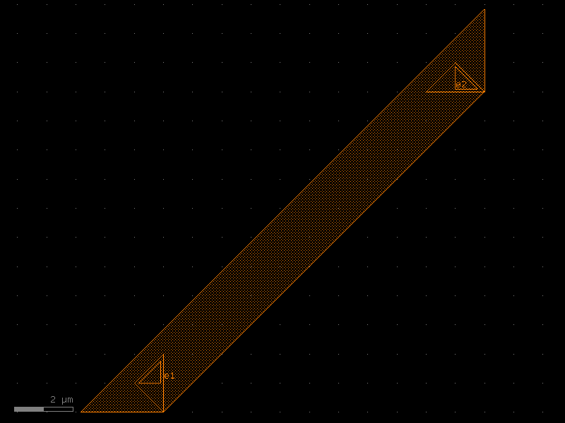
bend_metal#
- ihp.cells2.bend_metal(radius=None, angle=90, width=None, cross_section='metal_routing')[source]#
Regular degree euler bend.
- Parameters:
radius (float | None)
angle (float)
width (float | None)
cross_section (CrossSection | str | dict[str, Any] | Callable[[...], CrossSection] | SymmetricalCrossSection | DCrossSection)
- Return type:
Component
import warnings
warnings.filterwarnings("ignore", category=DeprecationWarning)

from ihp import PDK
from ihp import cells2

PDK.activate()

c = cells2.bend_metal(angle=90, cross_section='metal_routing').copy()
c.draw_ports()
c.plot()
(Source code, png, hires.png, pdf)
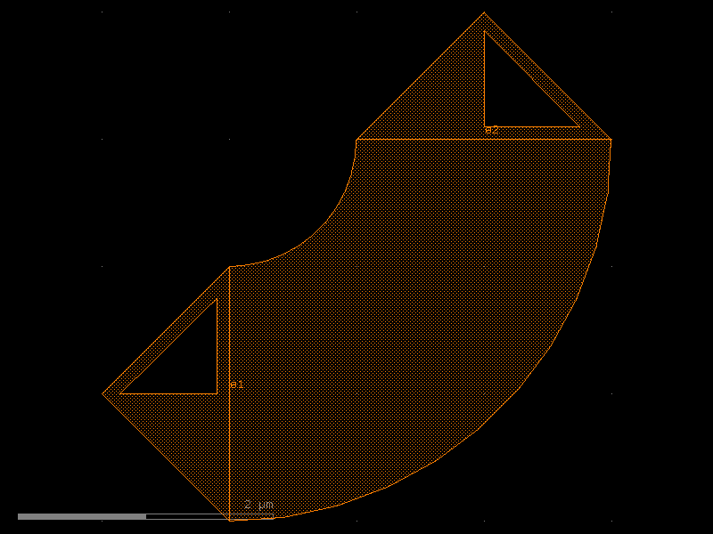
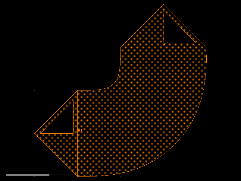
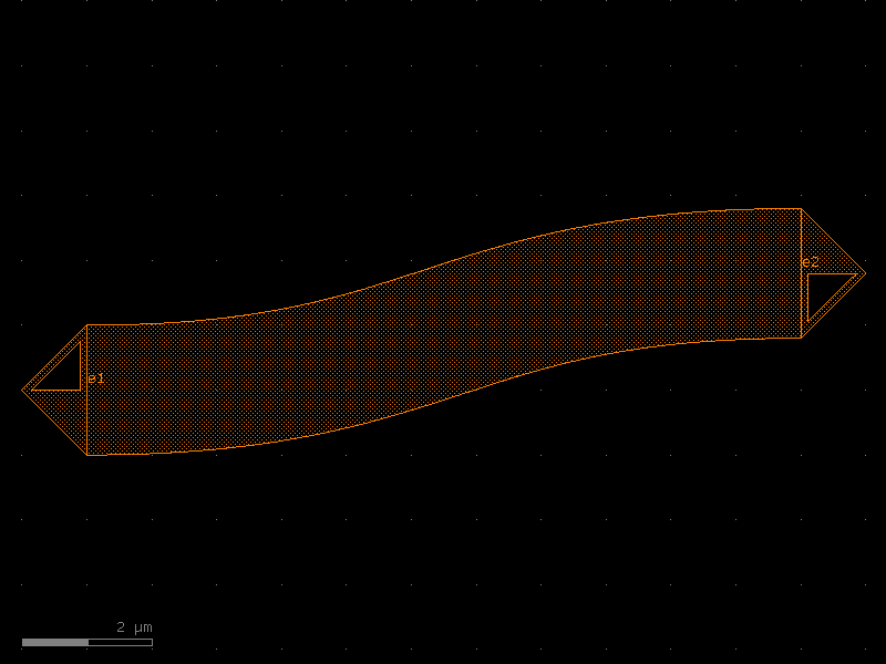
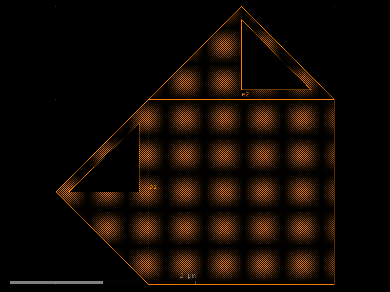
bend_s#
- ihp.cells2.bend_s(size=(11, 1.8), cross_section='strip', width=None, allow_min_radius_violation=False)[source]#
Return S bend with bezier curve.
stores min_bend_radius property in self.info[‘min_bend_radius’] min_bend_radius depends on height and length
- Parameters:
size (tuple[float, float]) – in x and y direction.
cross_section (CrossSection | str | dict[str, Any] | Callable[[...], CrossSection] | SymmetricalCrossSection | DCrossSection) – spec.
width (float | None) – width of the waveguide. If None, it will use the width of the cross_section.
allow_min_radius_violation (bool) – allows min radius violations.
- Return type:
Component
import warnings
warnings.filterwarnings("ignore", category=DeprecationWarning)

from ihp import PDK
from ihp import cells2

PDK.activate()

c = cells2.bend_s(size=(11, 1.8), cross_section='strip', allow_min_radius_violation=False).copy()
c.draw_ports()
c.plot()
(Source code, png, hires.png, pdf)

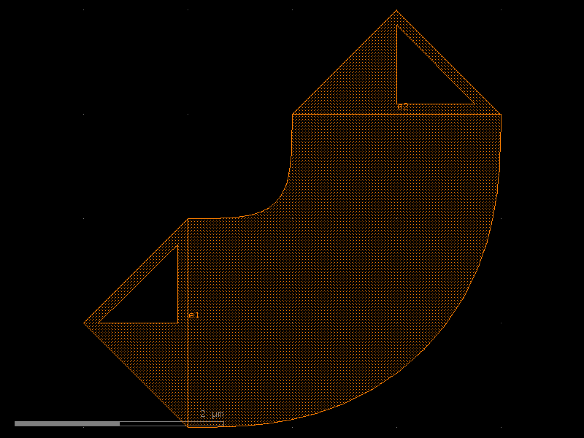
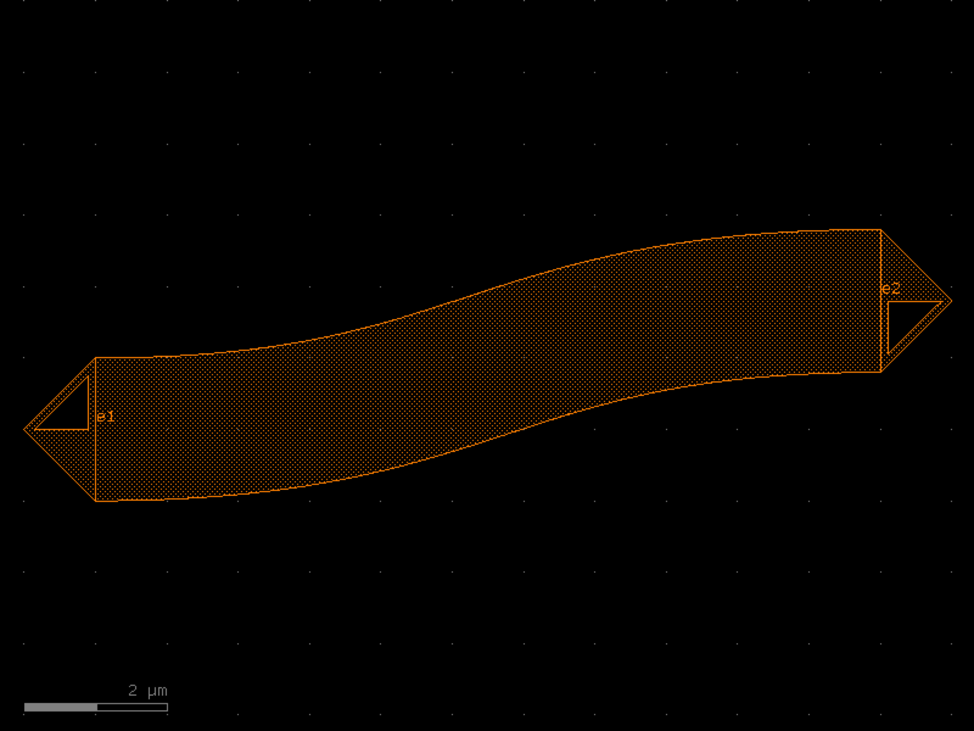
bend_s_metal#
- ihp.cells2.bend_s_metal(size=(11, 1.8), cross_section='metal_routing', width=None, allow_min_radius_violation=True)[source]#
Return S bend with bezier curve.
stores min_bend_radius property in self.info[‘min_bend_radius’] min_bend_radius depends on height and length
- Parameters:
size (tuple[float, float]) – in x and y direction.
cross_section (CrossSection | str | dict[str, Any] | Callable[[...], CrossSection] | SymmetricalCrossSection | DCrossSection) – spec.
width (float | None) – width of the waveguide. If None, it will use the width of the cross_section.
allow_min_radius_violation (bool) – allows min radius violations.
- Return type:
Component
import warnings
warnings.filterwarnings("ignore", category=DeprecationWarning)

from ihp import PDK
from ihp import cells2

PDK.activate()

c = cells2.bend_s_metal(size=(11, 1.8), cross_section='metal_routing', allow_min_radius_violation=True).copy()
c.draw_ports()
c.plot()
(Source code, png, hires.png, pdf)

bondpad#
- ihp.cells2.bondpad(shape='octagon', stack='t', fillMetals='nil', flipChip='no', diameter=80.0, hwQuota=1, topMetal='TM2', bottomMetal='3', addFillerEx='nil', passEncl=2.1, padType='bondpad')[source]#
Create a bondpad for wire bonding or flip-chip connection.
This function generates a parametric bondpad with configurable shape, metal stack, size, passivation, filler, and flip-chip options.
- Parameters:
shape (Literal['octagon', 'square', 'circle']) – Shape of the bondpad. Options: ‘octagon’, ‘square’, ‘circle’.
stack (Literal['t', 'nil']) – Stack all metal layers from bottom to top (‘t’ or ‘nil’).
fillMetals (Literal['t', 'nil']) – Add metal fill patterns (‘t’ for yes, ‘nil’ for no).
flipChip (Literal['yes', 'no']) – Enable flip-chip configuration (‘yes’ or ‘no’).
diameter (float) – Diameter or size of the bondpad in micrometers.
hwQuota (float) – Height/width quota for pad design rules.
topMetal (Literal['TM1', 'TM2']) – Name of the top metal layer. Options: ‘TM1’, ‘TM2’.
bottomMetal (Literal['1', '2', '3', '4', '5', 'TM1']) – Name of the bottom metal layer. Options: ‘1’, ‘2’, ‘3’, ‘4’, ‘5’, ‘TM1’.
addFillerEx (Literal['t', 'nil']) – Exclude metal filler (‘t’ or ‘nil’).
passEncl (float) – Passivation enclosure around the pad, in micrometers.
padType (Literal['bondpad', 'probepad']) – Type of pad. Options: ‘bondpad’, ‘probepad’.
- Returns:
The generated bondpad layout.
- Return type:
gdsfactory.Component
import warnings
warnings.filterwarnings("ignore", category=DeprecationWarning)

from ihp import PDK
from ihp import cells2

PDK.activate()

c = cells2.bondpad(shape='octagon', stack='t', fillMetals='nil', flipChip='no', diameter=80.0, hwQuota=1, topMetal='TM2', bottomMetal='3', addFillerEx='nil', passEncl=2.1, padType='bondpad').copy()
c.draw_ports()
c.plot()
(Source code, png, hires.png, pdf)

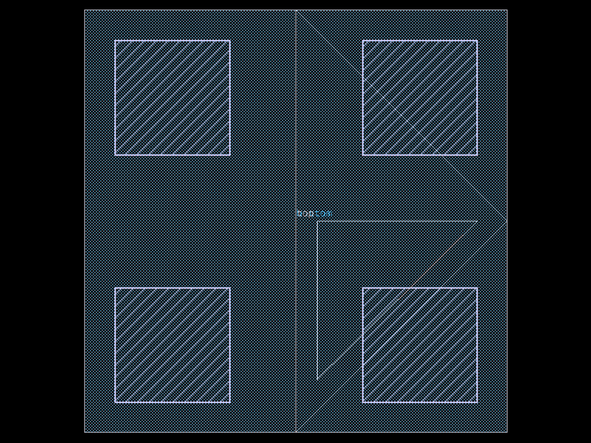
bondpad_array#
- ihp.cells2.bondpad_array(n_pads=4, pad_pitch=100.0, pad_diameter=68.0, shape='octagon', stack_metals='t')[source]#
Create an array of bondpads.
- Parameters:
n_pads (int) – Number of bondpads.
pad_pitch (float) – Pitch between bondpad centers in micrometers.
pad_diameter (float) – Diameter of each bondpad in micrometers.
shape (Literal['octagon', 'square', 'circle']) – Shape of the bondpads.
stack_metals (Literal['t', 'nil']) – Stack all metal layers.
- Returns:
Component with bondpad array.
- Return type:
Component
import warnings
warnings.filterwarnings("ignore", category=DeprecationWarning)

from ihp import PDK
from ihp import cells2

PDK.activate()

c = cells2.bondpad_array(n_pads=4, pad_pitch=100.0, pad_diameter=68.0, shape='octagon', stack_metals='t').copy()
c.draw_ports()
c.plot()
(Source code, png, hires.png, pdf)

cmim#
- ihp.cells2.cmim(width=6.99, length=6.99, guardRingType='none', guardRingDistance=1)[source]#
Create a MIM (Metal-Insulator-Metal) capacitor.
This function generates a layout cell for a MIM capacitor with optional guard rings. The capacitor dimensions and the spacing to the guard ring can be customized.
- Parameters:
width (float) – Width of the capacitor in micrometers.
length (float) – Length of the capacitor in micrometers.
guardRingType (Literal['none', 'psub', 'nwell']) – Type of guard ring to include. Options: - ‘none’: No guard ring. - ‘psub’: P-substrate guard ring surrounding the capacitor. - ‘nwell’: N-well guard ring surrounding the capacitor.
guardRingDistance (float) – Spacing between the capacitor body and the guard ring, in micrometers.
- Returns:
The generated MIM capacitor layout.
- Return type:
gdsfactory.Component
import warnings
warnings.filterwarnings("ignore", category=DeprecationWarning)

from ihp import PDK
from ihp import cells2

PDK.activate()

c = cells2.cmim(width=6.99, length=6.99, guardRingType='none', guardRingDistance=1).copy()
c.draw_ports()
c.plot()
(Source code, png, hires.png, pdf)
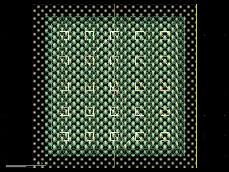
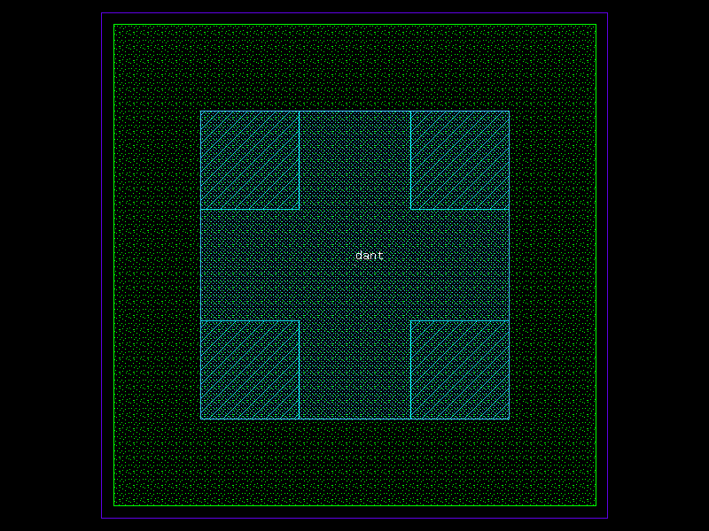
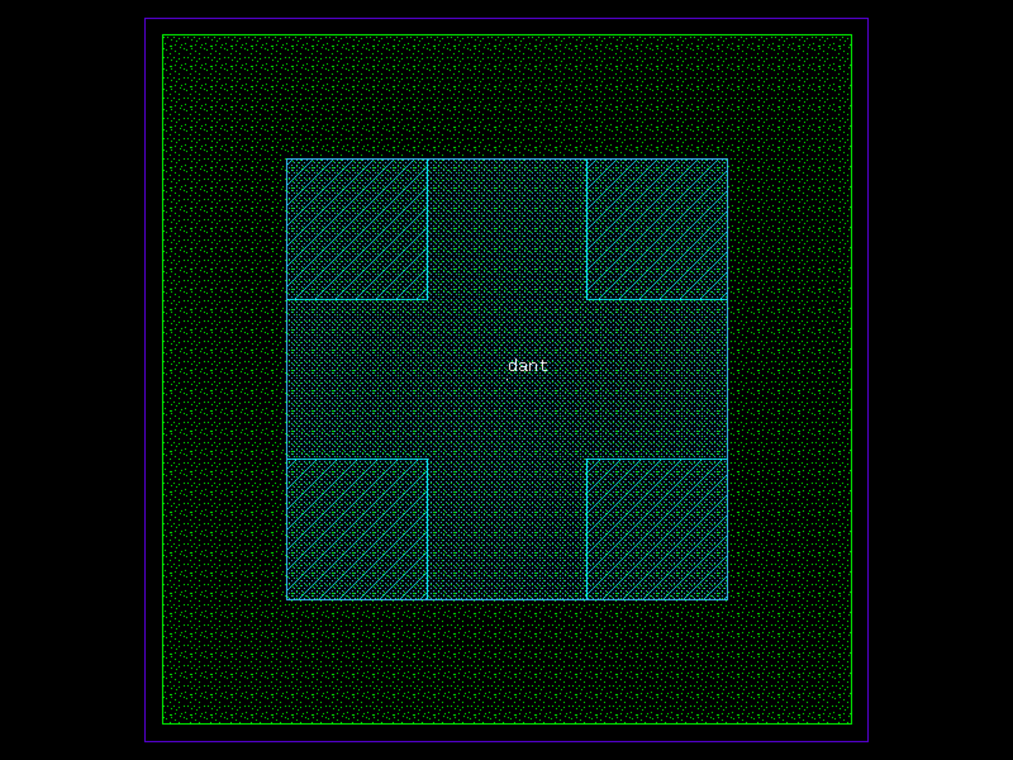
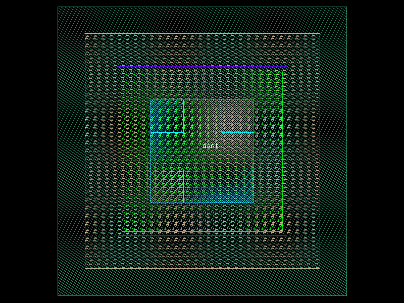
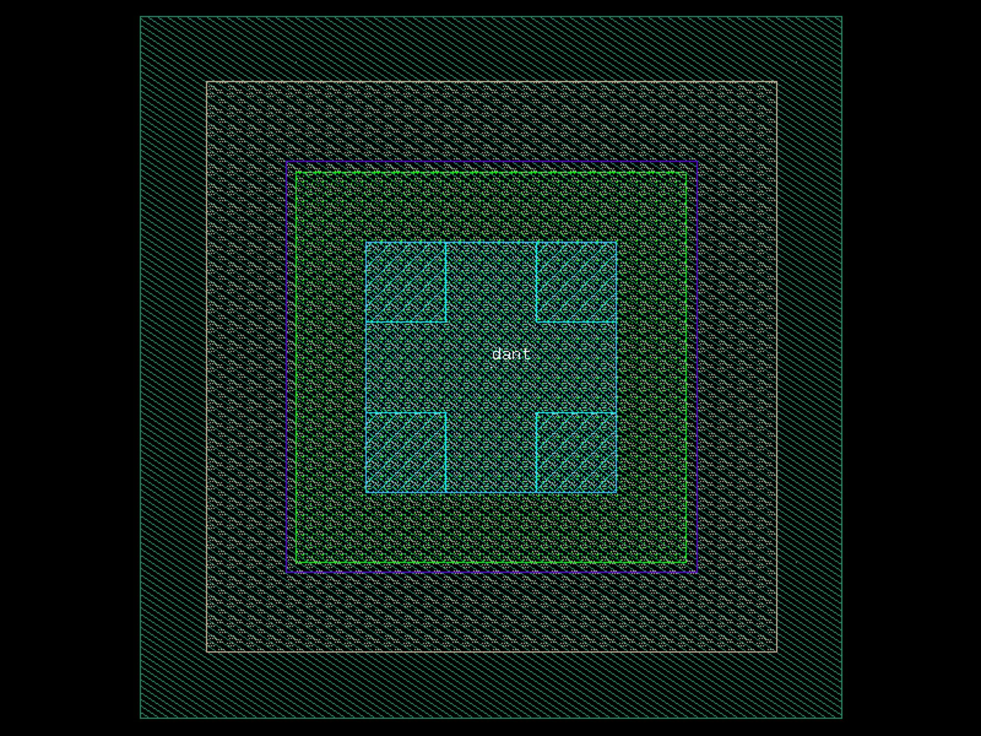
dantenna#
- ihp.cells2.dantenna(width=0.78, length=0.78, addRecLayer='t', guardRingType='none', guardRingDistance=1)[source]#
Creates a diode antenna (dantenna) structure.
This function generates a layout cell containing a rectangular antenna region with optional recognition layers and guard ring structures. Parameters allow customization of the antenna geometry and the type and spacing of guard rings.
- Parameters:
width (float) – Width of the antenna rectangle in microns.
length (float) – Length of the antenna rectangle in microns.
addRecLayer (str) – Recognition layer to add (e.g., ‘t’ for top, ‘b’ for bottom, or ‘’ for none).
guardRingType (Literal['none', 'psub']) – Type of guard ring to include. Options include: - ‘none’: No guard ring - ‘psub’: P-type guard ring
guardRingDistance (float) – Spacing between the antenna body and guard ring in microns.
- Returns:
The generated antenna component.
- Return type:
gdsfactory.Component
import warnings
warnings.filterwarnings("ignore", category=DeprecationWarning)

from ihp import PDK
from ihp import cells2

PDK.activate()

c = cells2.dantenna(width=0.78, length=0.78, addRecLayer='t', guardRingType='none', guardRingDistance=1).copy()
c.draw_ports()
c.plot()
(Source code, png, hires.png, pdf)

dpantenna#
- ihp.cells2.dpantenna(width=0.78, length=0.78, addRecLayer='t', guardRingType='none', guardRingDistance=1)[source]#
Creates a dual-polarity antenna (dpantenna) structure.
Generates a layout cell containing a rectangular antenna region with an optional recognition layer and an optional n-well guard ring. Parameters allow customization of the antenna geometry and the spacing between the antenna body and the surrounding guard ring.
- Parameters:
width (float) – Width of the antenna rectangle in microns.
length (float) – Length of the antenna rectangle in microns.
addRecLayer (Literal['t', 'f']) – Whether to add a recognition layer. Valid values: - ‘t’: Add recognition layer. - ‘f’: Do not add a recognition layer.
guardRingType (Literal['none', 'nwell']) – Type of guard ring to include. Valid values: - ‘none’: No guard ring. - ‘nwell’: Surrounding n-well guard ring.
guardRingDistance (float) – Spacing between the antenna body and the n-well guard ring, in microns.
- Returns:
The generated antenna component.
- Return type:
gdsfactory.Component
import warnings
warnings.filterwarnings("ignore", category=DeprecationWarning)

from ihp import PDK
from ihp import cells2

PDK.activate()

c = cells2.dpantenna(width=0.78, length=0.78, addRecLayer='t', guardRingType='none', guardRingDistance=1).copy()
c.draw_ports()
c.plot()
(Source code, png, hires.png, pdf)

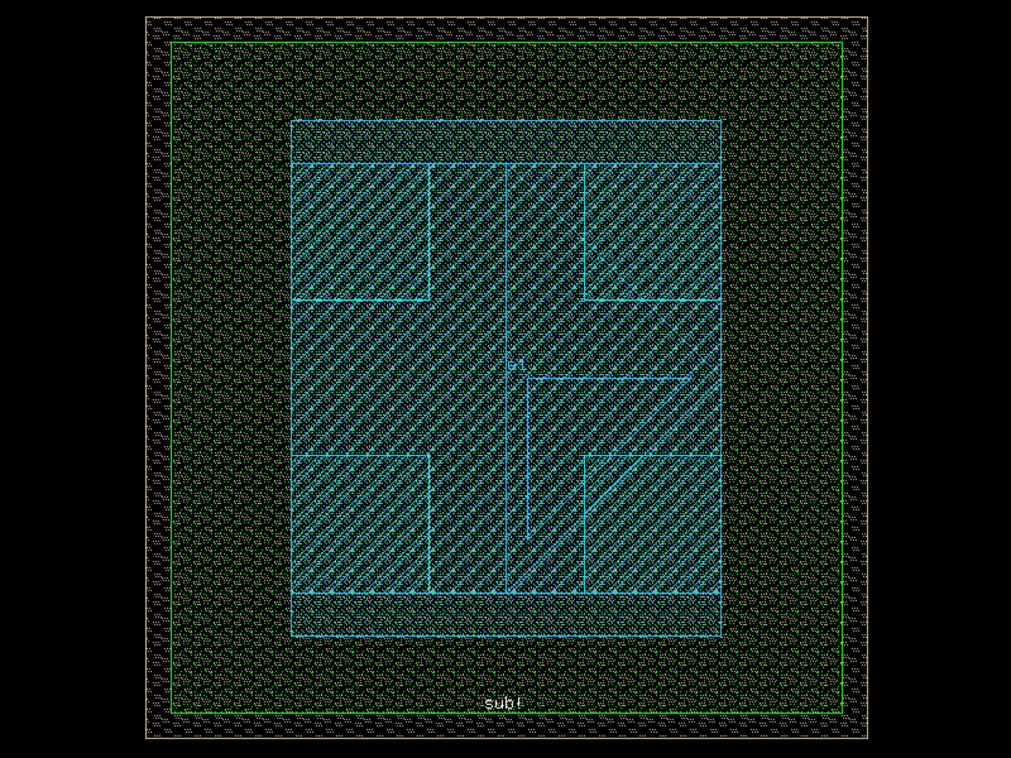
esd#
- ihp.cells2.esd(model='diodevdd_2kv')[source]#
Create an ESD protection device layout.
This function generates an electrostatic discharge (ESD) protection device using the specified model. Available models include diodes and NMOS clamps for different voltage ratings.
- Parameters:
model (Literal['diodevdd_2kv', 'diodevss_2kv', 'diodevdd_4kv', 'diodevss_4kv', 'nmoscl_2', 'nmoscl_4']) – Device model name. Options: - ‘diodevdd_2kv’: Diode from VDD for 2 kV rating. - ‘diodevss_2kv’: Diode to VSS for 2 kV rating. - ‘diodevdd_4kv’: Diode from VDD for 4 kV rating. - ‘diodevss_4kv’: Diode to VSS for 4 kV rating. - ‘nmoscl_2’: NMOS clamp for 2 kV rating. - ‘nmoscl_4’: NMOS clamp for 4 kV rating.
- Returns:
The generated ESD protection layout.
- Return type:
gdsfactory.Component
import warnings
warnings.filterwarnings("ignore", category=DeprecationWarning)

from ihp import PDK
from ihp import cells2

PDK.activate()

c = cells2.esd(model='diodevdd_2kv').copy()
c.draw_ports()
c.plot()
generate_gf_from_ihp#
- ihp.cells2.generate_gf_from_ihp(cell_name, cell_params, function_name)[source]#
- Return type:
Component
import warnings
warnings.filterwarnings("ignore", category=DeprecationWarning)

from ihp import PDK
from ihp import cells2

PDK.activate()

c = cells2.generate_gf_from_ihp().copy()
c.draw_ports()
c.plot()
inductor2#
- ihp.cells2.inductor2(width=2, space=2.1, distance=15.48, resistance=1, inductance=1, num_turns=1, block_qrc=True, subE=False, guardRingType='none', guardRingDistance=1)[source]#
Create a parametric inductor layout.
This function generates a planar inductor with customizable width, spacing, number of turns, and optional guard rings. The layout can also include blocking of QRC structures and substrate connections.
- Parameters:
width (float) – Width of the inductor trace in micrometers.
space (float) – Spacing between turns of the inductor in micrometers.
distance (float) – Total distance of the inductor layout in micrometers.
resistance (float) – Target series resistance in Ohms.
inductance (float) – Target inductance in nH (used for layout optimization).
num_turns (int) – Number of turns in the inductor.
block_qrc (bool) – Whether to block QRC (quasi-resistor-capacitor) structures.
subE (bool) – Whether to connect to substrate for shielding or grounding.
guardRingType (Literal['none', 'psub', 'nwell']) – Type of guard ring to include. Options: - ‘none’: No guard ring. - ‘psub’: P-substrate guard ring. - ‘nwell’: N-well guard ring.
guardRingDistance (float) – Spacing between the inductor and the guard ring, in micrometers.
- Returns:
The generated inductor layout.
- Return type:
gdsfactory.Component
import warnings
warnings.filterwarnings("ignore", category=DeprecationWarning)

from ihp import PDK
from ihp import cells2

PDK.activate()

c = cells2.inductor2(width=2, space=2.1, distance=15.48, resistance=1, inductance=1, num_turns=1, block_qrc=True, subE=False, guardRingType='none', guardRingDistance=1).copy()
c.draw_ports()
c.plot()
inductor3#
- ihp.cells2.inductor3(width=2, space=2.1, distance=25.84, resistance=1, inductance=1, num_turns=2, block_qrc=True, subE=False, guardRingType='none', guardRingDistance=1)[source]#
Create a parametric inductor layout.
This function generates a planar inductor with customizable width, spacing, total distance, number of turns, and optional guard rings. The layout can also include blocking of QRC structures and substrate connections.
- Parameters:
width (float) – Width of the inductor trace in micrometers.
space (float) – Spacing between turns of the inductor in micrometers.
distance (float) – Total distance of the inductor layout in micrometers.
resistance (float) – Target series resistance in Ohms.
inductance (float) – Target inductance in nH (used for layout optimization).
num_turns (int) – Number of turns in the inductor.
block_qrc (bool) – Whether to block QRC (quasi-resistor-capacitor) structures.
subE (bool) – Whether to connect to substrate for shielding or grounding.
guardRingType (Literal['none', 'psub', 'nwell']) – Type of guard ring to include. Options: - ‘none’: No guard ring. - ‘psub’: P-substrate guard ring. - ‘nwell’: N-well guard ring.
guardRingDistance (float) – Spacing between the inductor and the guard ring, in micrometers.
- Returns:
The generated inductor layout.
- Return type:
gdsfactory.Component
import warnings
warnings.filterwarnings("ignore", category=DeprecationWarning)

from ihp import PDK
from ihp import cells2

PDK.activate()

c = cells2.inductor3(width=2, space=2.1, distance=25.84, resistance=1, inductance=1, num_turns=2, block_qrc=True, subE=False, guardRingType='none', guardRingDistance=1).copy()
c.draw_ports()
c.plot()
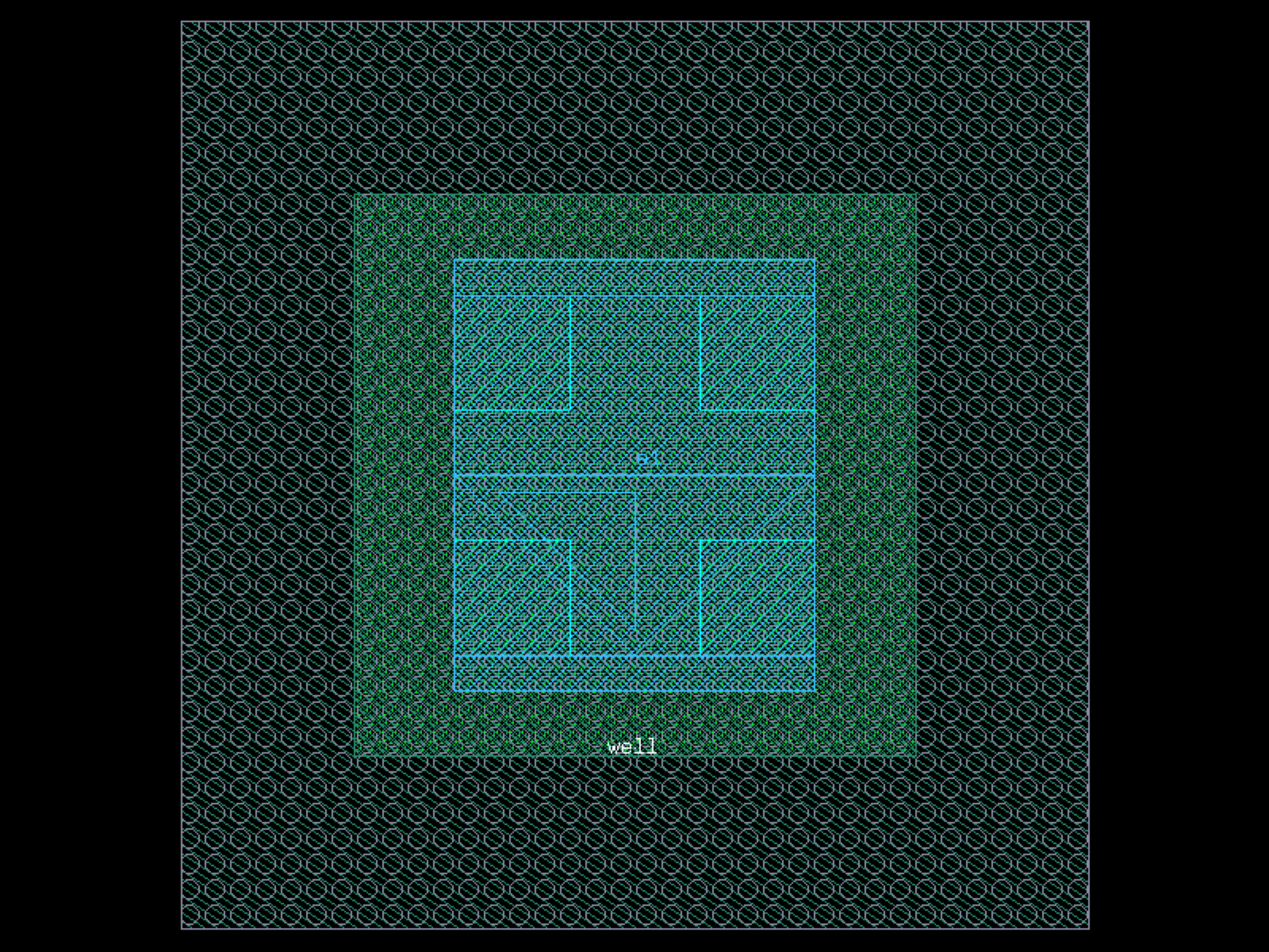
nmos#
- ihp.cells2.nmos(w=0.15, l=0.13, ng=1, guardRingType='none', guardRingDistance=1)[source]#
Create an NMOS transistor layout.
This function generates a parametric NMOS transistor with configurable width, length, number of gates/fingers, and optional P-substrate guard ring.
- Parameters:
w (float) – Total width of the transistor in micrometers.
l (float) – Length of the transistor in micrometers.
ng (int) – Number of gates/fingers.
guardRingType (Literal['none', 'psub']) – Type of guard ring to include. Options: - ‘none’: No guard ring. - ‘psub’: P-substrate guard ring.
guardRingDistance (float) – Spacing between the transistor and the guard ring, in micrometers.
- Returns:
The generated NMOS transistor layout.
- Return type:
gdsfactory.Component
import warnings
warnings.filterwarnings("ignore", category=DeprecationWarning)

from ihp import PDK
from ihp import cells2

PDK.activate()

c = cells2.nmos(w=0.15, l=0.13, ng=1, guardRingType='none', guardRingDistance=1).copy()
c.draw_ports()
c.plot()
(Source code, png, hires.png, pdf)
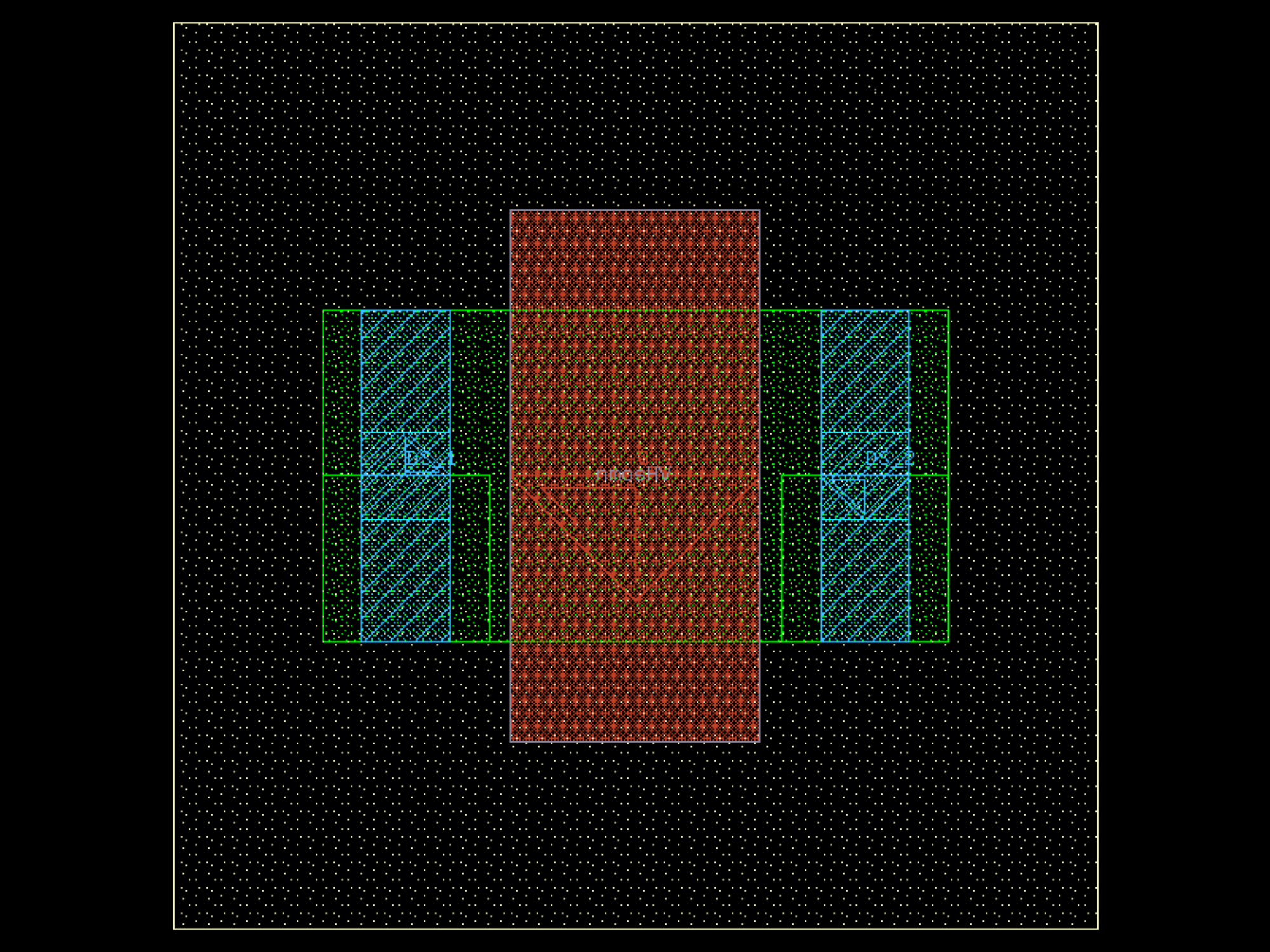
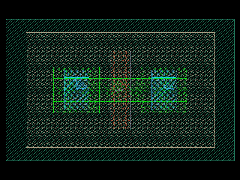
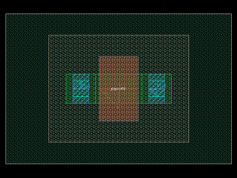
nmosHV#
- ihp.cells2.nmosHV(w=0.6, l=0.45, ng=1, guardRingType='none', guardRingDistance=1)[source]#
Create a high-voltage NMOS transistor layout.
This function generates a parametric high-voltage NMOS transistor with configurable width, length, number of gates/fingers, and optional P-substrate guard ring.
- Parameters:
w (float) – Total width of the transistor in micrometers.
l (float) – Length of the transistor in micrometers.
ng (int) – Number of gates/fingers.
guardRingType (Literal['none', 'psub']) – Type of guard ring to include. Options: - ‘none’: No guard ring. - ‘psub’: P-substrate guard ring.
guardRingDistance (float) – Spacing between the transistor and the guard ring, in micrometers.
- Returns:
The generated high-voltage NMOS transistor layout.
- Return type:
gdsfactory.Component
import warnings
warnings.filterwarnings("ignore", category=DeprecationWarning)

from ihp import PDK
from ihp import cells2

PDK.activate()

c = cells2.nmosHV(w=0.6, l=0.45, ng=1, guardRingType='none', guardRingDistance=1).copy()
c.draw_ports()
c.plot()
(Source code, png, hires.png, pdf)

no_filler_stack#
- ihp.cells2.no_filler_stack(width=10, length=10, noAct='Yes', noGP='Yes', noM1='Yes', noM2='Yes', noM3='Yes', noM4='Yes', noM5='Yes', noTM1='Yes', noTM2='Yes')[source]#
Create a NoFiller via stack test component.
This function generates a via stack layout without filler structures for the selected layers. Each layer can be individually excluded from filler insertion using Yes/No flags.
- Parameters:
width (int) – Device width in micrometers.
length (int) – Device length in micrometers.
noAct (Literal['Yes', 'No']) – Exclude filler for the active layer. Options: ‘Yes’, ‘No’.
noGP (Literal['Yes', 'No']) – Exclude filler for the GatePoly layer. Options: ‘Yes’, ‘No’.
noM1 (Literal['Yes', 'No']) – Exclude filler for Metal1. Options: ‘Yes’, ‘No’.
noM2 (Literal['Yes', 'No']) – Exclude filler for Metal2. Options: ‘Yes’, ‘No’.
noM3 (Literal['Yes', 'No']) – Exclude filler for Metal3. Options: ‘Yes’, ‘No’.
noM4 (Literal['Yes', 'No']) – Exclude filler for Metal4. Options: ‘Yes’, ‘No’.
noM5 (Literal['Yes', 'No']) – Exclude filler for Metal5. Options: ‘Yes’, ‘No’.
noTM1 (Literal['Yes', 'No']) – Exclude filler for TopMetal1. Options: ‘Yes’, ‘No’.
noTM2 (Literal['Yes', 'No']) – Exclude filler for TopMetal2. Options: ‘Yes’, ‘No’.
- Returns:
The generated NoFiller via stack layout.
- Return type:
gdsfactory.Component
import warnings
warnings.filterwarnings("ignore", category=DeprecationWarning)

from ihp import PDK
from ihp import cells2

PDK.activate()

c = cells2.no_filler_stack(width=10, length=10, noAct='Yes', noGP='Yes', noM1='Yes', noM2='Yes', noM3='Yes', noM4='Yes', noM5='Yes', noTM1='Yes', noTM2='Yes').copy()
c.draw_ports()
c.plot()
(Source code, png, hires.png, pdf)

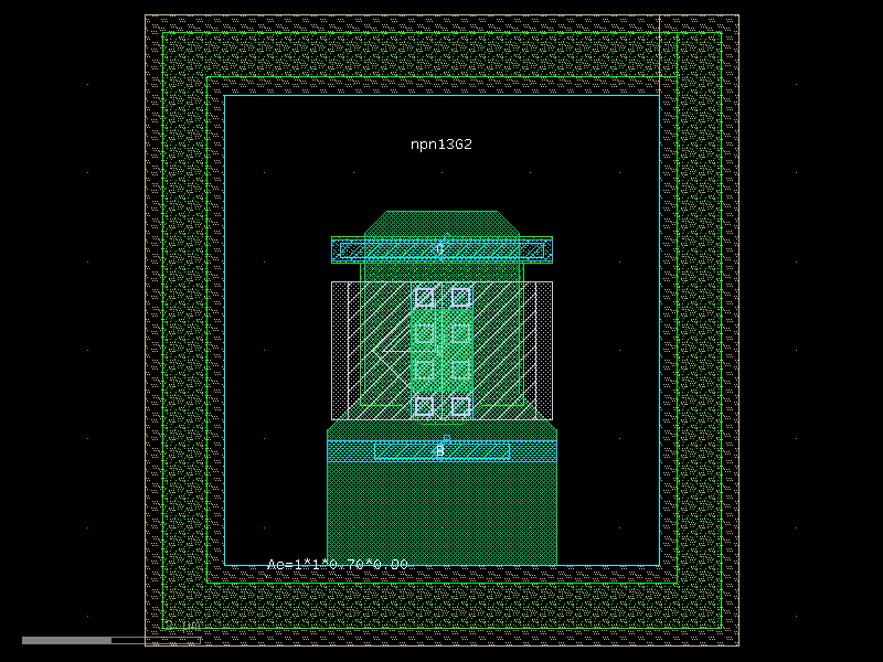
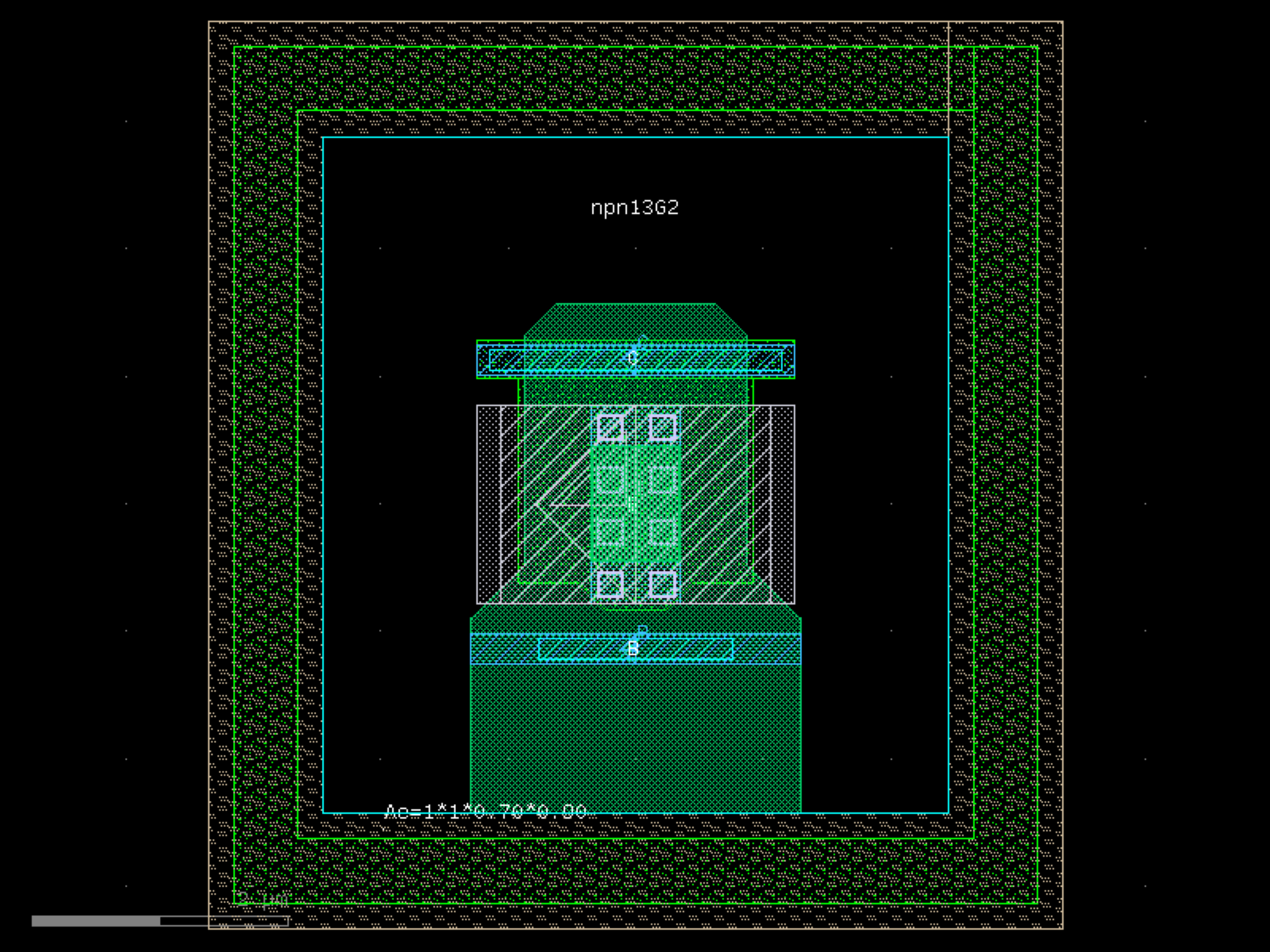
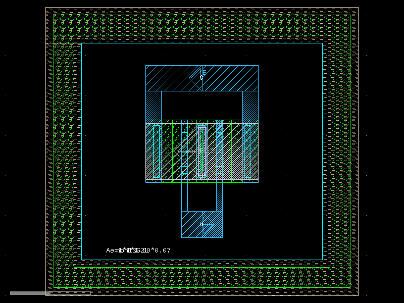
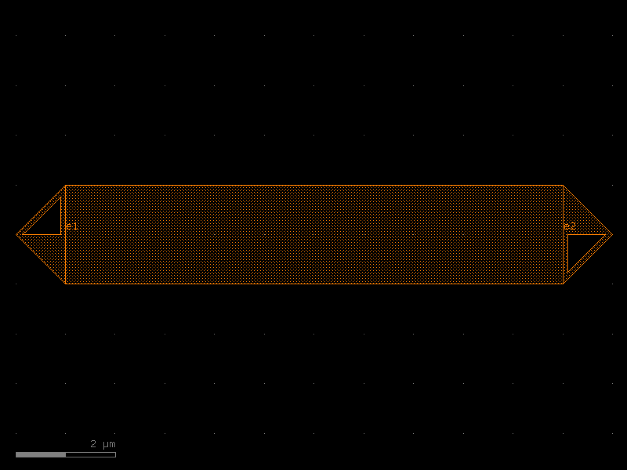
npn13G2#
- ihp.cells2.npn13G2(STI=0.44, baspolyx=0.3, bipwinx=0.07, bipwiny=0.1, empolyx=0.15, empolyy=0.18, emitter_length=0.9, emitter_width=0.7, Nx=1, Ny=1, text='npn13G2', CMetY1=0, CMetY2=0)[source]#
Returns the IHP npn13G2 BJT transistor as a gdsfactory Component.
This function generates a parametric layout of the npn13G2 heterojunction bipolar transistor (HBT) from the IHP SG13G2 process. Geometry parameters control the emitter, base, and implant enclosure sizes, while Nx and Ny define the emitter finger array configuration.
- Parameters:
STI (float) – STI enclosure around the active device, in microns.
baspolyx (float) – Base poly enclosure in the x-direction, in microns.
bipwinx (float) – BIP window enclosure in the x-direction, in microns.
bipwiny (float) – BIP window enclosure in the y-direction, in microns.
empolyx (float) – Emitter poly enclosure in the x-direction, in microns.
empolyy (float) – Emitter poly enclosure in the y-direction, in microns.
emitter_length (float) – Length of each emitter finger, in microns.
emitter_width (float) – Width of each emitter finger, in microns.
Nx (int) – Number of emitter fingers.
Ny (int) – Number of emitter rows (not used by current IHP PyCell implementation).
text (str) – Label text to place on the device.
CMetY1 (float) – Optional metal extension on the collector side (lower side), in microns.
CMetY2 (float) – Optional metal extension on the collector side (upper side), in microns.
- Returns:
The generated npn13G2 transistor layout.
- Return type:
gdsfactory.Component
import warnings
warnings.filterwarnings("ignore", category=DeprecationWarning)

from ihp import PDK
from ihp import cells2

PDK.activate()

c = cells2.npn13G2(STI=0.44, baspolyx=0.3, bipwinx=0.07, bipwiny=0.1, empolyx=0.15, empolyy=0.18, emitter_length=0.9, emitter_width=0.7, Nx=1, Ny=1, text='npn13G2', CMetY1=0, CMetY2=0).copy()
c.draw_ports()
c.plot()
(Source code, png, hires.png, pdf)

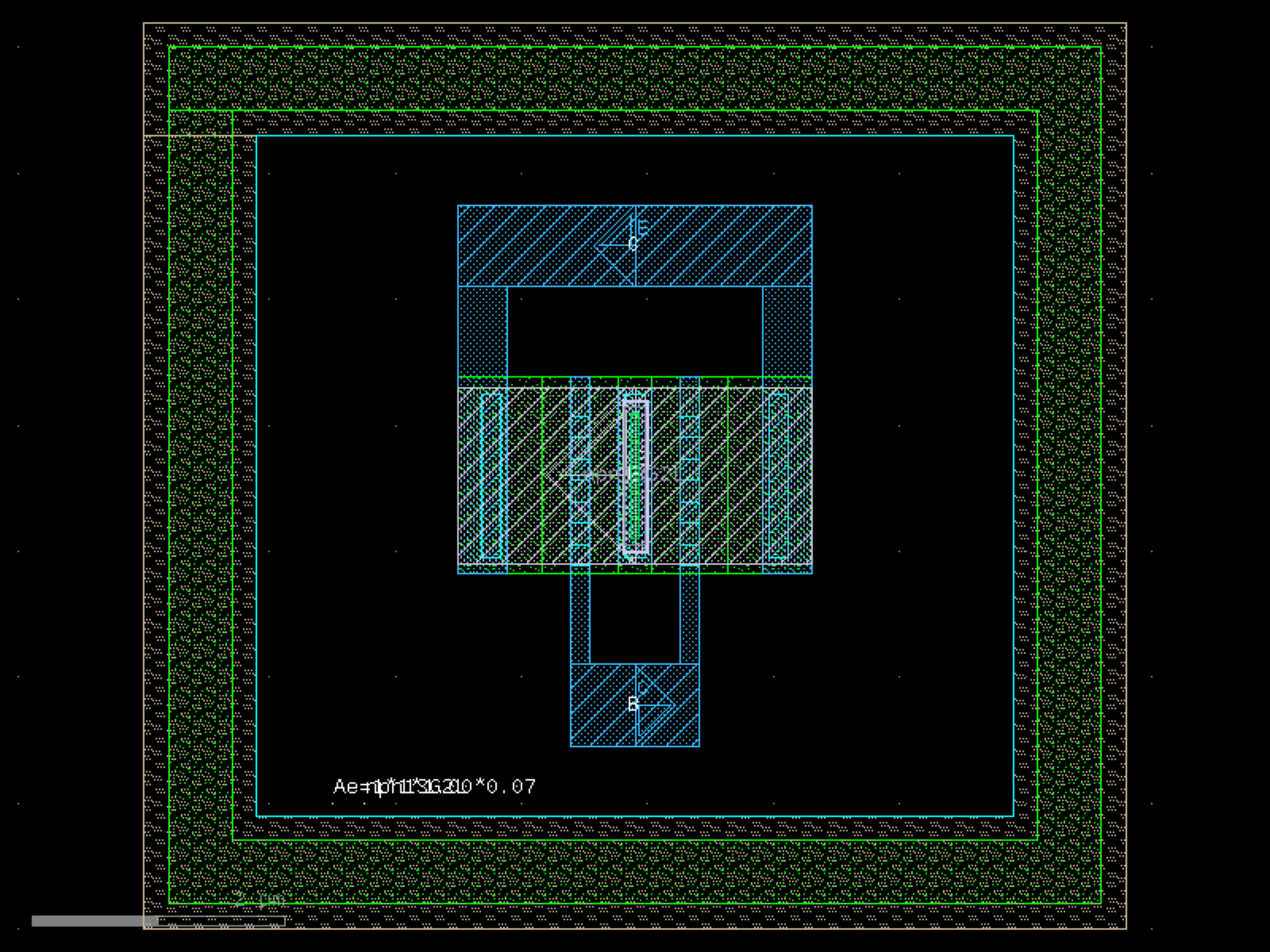
npn13G2L#
- ihp.cells2.npn13G2L(Nx=1, emitter_length=1, emitter_width=0.07)[source]#
Returns the IHP npn13G2L BJT transistor as a gdsfactory Component.
This function generates a layout for the npn13G2L heterojunction bipolar transistor (HBT) from the IHP SG13G2 process. The transistor geometry is defined by the number of emitter fingers and the dimensions of each emitter finger.
- Parameters:
Nx (int) – Number of emitter fingers.
emitter_length (float) – Length of each emitter finger, in microns.
emitter_width (float) – Width of each emitter finger, in microns.
- Returns:
The generated npn13G2L transistor layout.
- Return type:
gdsfactory.Component
import warnings
warnings.filterwarnings("ignore", category=DeprecationWarning)

from ihp import PDK
from ihp import cells2

PDK.activate()

c = cells2.npn13G2L(Nx=1, emitter_length=1, emitter_width=0.07).copy()
c.draw_ports()
c.plot()
(Source code, png, hires.png, pdf)
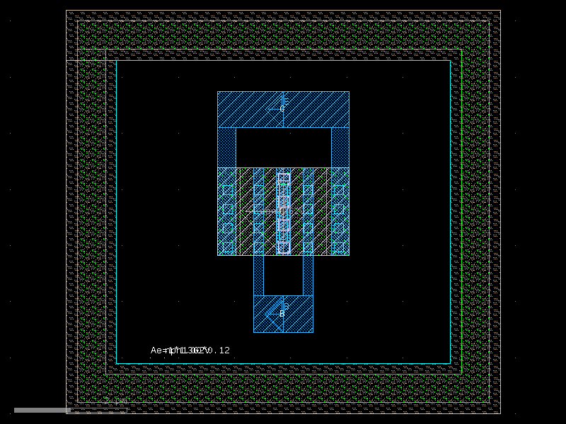
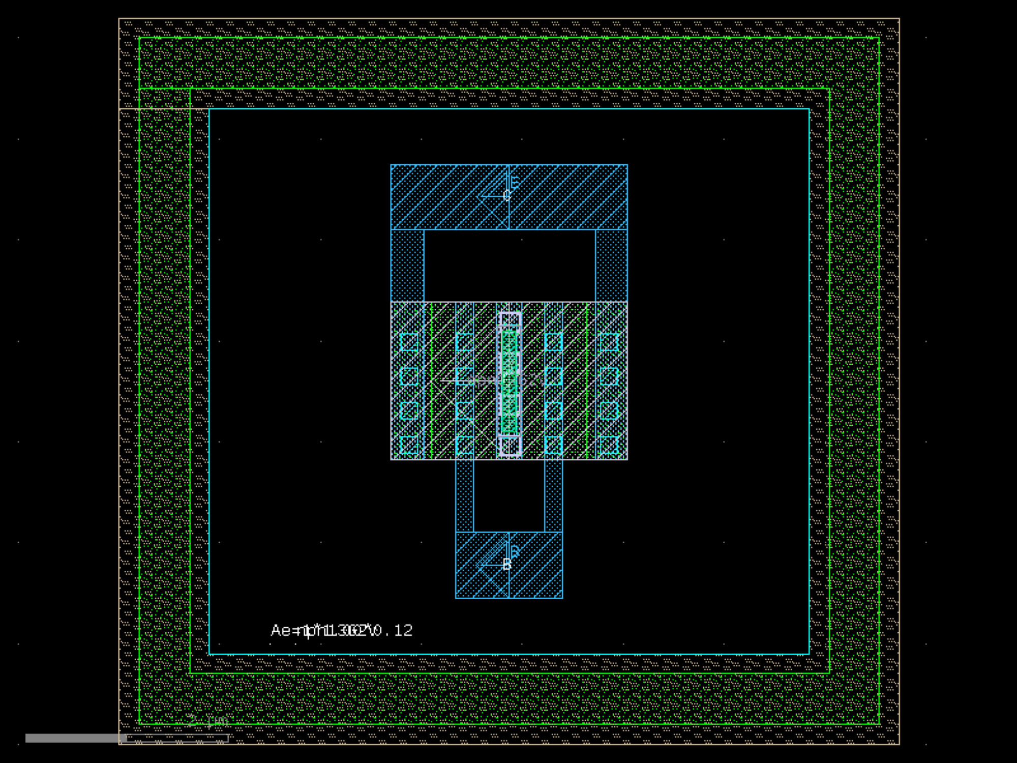
npn13G2V#
- ihp.cells2.npn13G2V(Nx=1, emitter_length=1, emitter_width=0.12)[source]#
Returns the IHP npn13G2V BJT transistor as a gdsfactory Component.
This function generates a layout for the npn13G2V heterojunction bipolar transistor (HBT) from the IHP SG13G2 process. The transistor geometry is defined by the number of emitter fingers and the dimensions of each emitter finger.
- Parameters:
Nx (int) – Number of emitter fingers. Valid range: [1, 8].
emitter_length (float) – Length of each emitter finger, in microns.
emitter_width (float) – Width of each emitter finger, in microns.
- Returns:
The generated npn13G2V transistor layout.
- Return type:
gdsfactory.Component
import warnings
warnings.filterwarnings("ignore", category=DeprecationWarning)

from ihp import PDK
from ihp import cells2

PDK.activate()

c = cells2.npn13G2V(Nx=1, emitter_length=1, emitter_width=0.12).copy()
c.draw_ports()
c.plot()
(Source code, png, hires.png, pdf)

ntap1#
- ihp.cells2.ntap1(width=0.78, length=0.78)[source]#
Create an N+ substrate tap.
- Parameters:
width – Width of the tap in micrometers.
length – Length of the tap in micrometers.
rows – Number of contact rows.
cols – Number of contact columns.
- Returns:
Component with N+ tap layout.
- Return type:
Component
import warnings
warnings.filterwarnings("ignore", category=DeprecationWarning)

from ihp import PDK
from ihp import cells2

PDK.activate()

c = cells2.ntap1(width=0.78, length=0.78).copy()
c.draw_ports()
c.plot()
(Source code, png, hires.png, pdf)

pack_doe#
- ihp.cells2.pack_doe(doe, settings, do_permutations=False, function=None, **kwargs)[source]#
Packs a component DOE (Design of Experiment) using pack.
- Parameters:
doe (str | Callable[[...], Component] | dict[str, Any] | DKCell | partial[Component]) – function to return Components.
settings (dict[str, tuple[Any, ...]]) – component settings.
do_permutations (bool) – for each setting.
function (str | Callable[[...], Component] | dict[str, Any] | None) – to apply (add padding, grating couplers).
kwargs – for pack.
- Keyword Arguments:
spacing – Minimum distance between adjacent shapes.
aspect_ratio – (width, height) ratio of the rectangular bin.
max_size – Limits the size into which the shapes will be packed.
sort_by_area – Pre-sorts the shapes by area.
density – Values closer to 1 pack tighter but require more computation.
precision – Desired precision for rounding vertex coordinates.
text – Optional function to add text labels.
text_prefix – for labels. For example. ‘A’ for ‘A1’, ‘A2’…
text_offsets – relative to component size info anchor. Defaults to center.
text_anchors – relative to component (ce cw nc ne nw sc se sw center cc).
name_prefix – for each packed component (avoids the Unnamed cells warning). Note that the suffix contains a uuid so the name will not be deterministic.
rotation – for each component in degrees.
h_mirror – horizontal mirror in y axis (x, 1) (1, 0). This is the most common.
v_mirror – vertical mirror using x axis (1, y) (0, y).
- Return type:
Component
import warnings
warnings.filterwarnings("ignore", category=DeprecationWarning)

from ihp import PDK
from ihp import cells2

PDK.activate()

c = cells2.pack_doe(do_permutations=False).copy()
c.draw_ports()
c.plot()
pack_doe_grid#
- ihp.cells2.pack_doe_grid(doe, settings, do_permutations=False, function=None, with_text=False, **kwargs)[source]#
Packs a component DOE (Design of Experiment) using grid.
- Parameters:
doe (str | Callable[[...], Component] | dict[str, Any] | DKCell | partial[Component]) – function to return Components.
settings (dict[str, tuple[Any, ...]]) – component settings.
do_permutations (bool) – for each setting.
function (str | Callable[[...], Component] | dict[str, Any] | None) – to apply to component (add padding, grating couplers).
with_text (bool) – includes text label.
kwargs – for grid.
- Keyword Arguments:
spacing – between adjacent elements on the grid, can be a tuple for different distances in height and width.
separation – If True, guarantees elements are separated with fixed spacing if False, elements are spaced evenly along a grid.
shape – x, y shape of the grid (see np.reshape). If no shape and the list is 1D, if np.reshape were run with (1, -1).
align_x – {‘x’, ‘xmin’, ‘xmax’} for x (column) alignment along.
align_y – {‘y’, ‘ymin’, ‘ymax’} for y (row) alignment along.
edge_x – {‘x’, ‘xmin’, ‘xmax’} for x (column) (ignored if separation = True).
edge_y – {‘y’, ‘ymin’, ‘ymax’} for y (row) (ignored if separation = True).
rotation – for each component in degrees.
h_mirror – horizontal mirror y axis (x, 1) (1, 0). most common mirror.
v_mirror – vertical mirror using x axis (1, y) (0, y).
- Return type:
Component
import warnings
warnings.filterwarnings("ignore", category=DeprecationWarning)

from ihp import PDK
from ihp import cells2

PDK.activate()

c = cells2.pack_doe_grid(do_permutations=False, with_text=False).copy()
c.draw_ports()
c.plot()
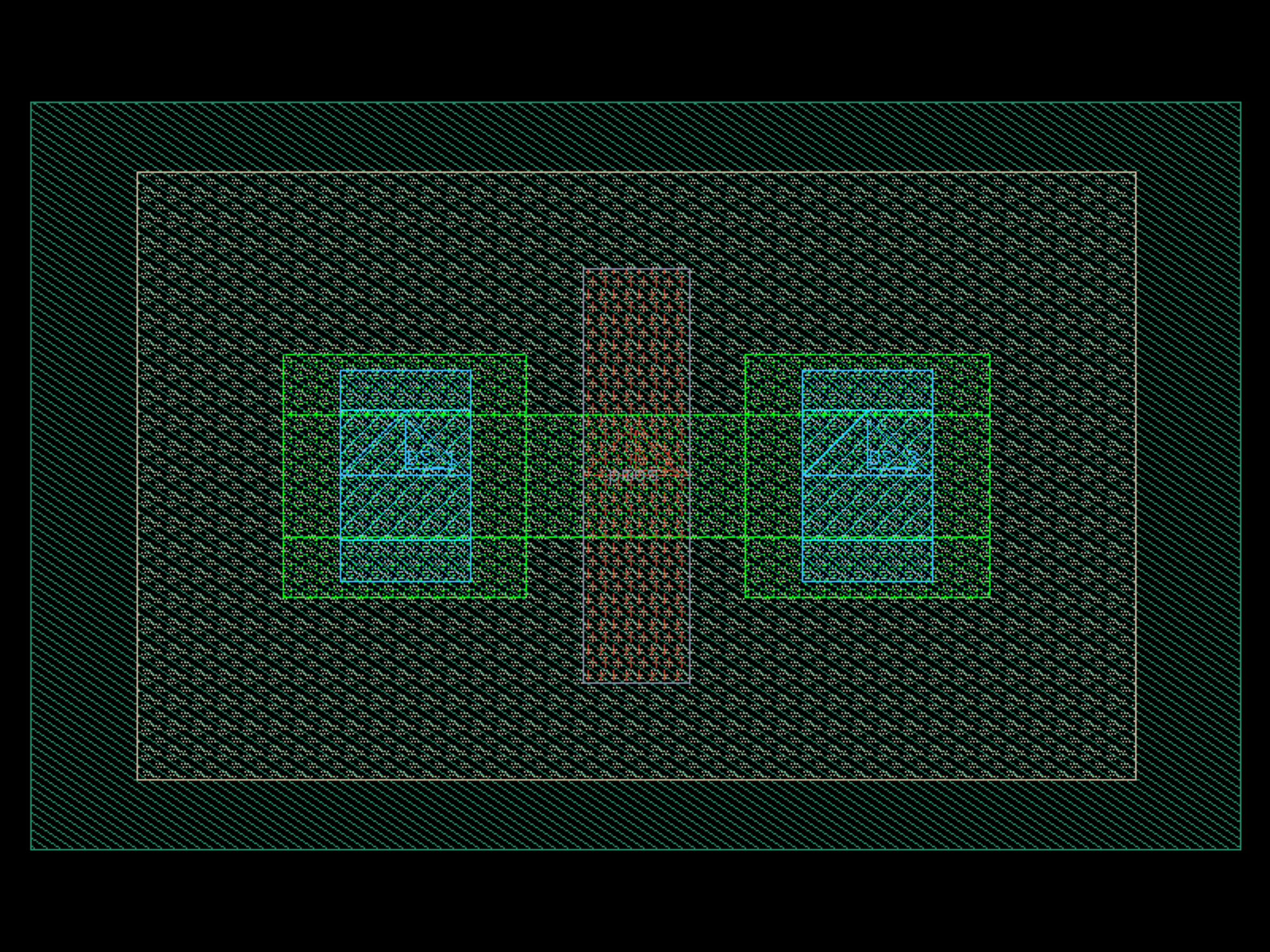
pmos#
- ihp.cells2.pmos(w=0.15, l=0.13, ng=1, guardRingType='none', guardRingDistance=1)[source]#
Create a PMOS transistor layout.
This function generates a parametric PMOS transistor with configurable width, length, number of gates/fingers, and optional guard ring.
- Parameters:
w (float) – Total width of the transistor in micrometers.
l (float) – Length of the transistor in micrometers.
ng (int) – Number of gates/fingers.
guardRingType (Literal['none', 'nwell']) – Type of guard ring to include. Options: - ‘none’: No guard ring. - ‘nwell’: N-well guard ring.
guardRingDistance (float) – Spacing between the transistor and the guard ring, in micrometers.
- Returns:
The generated PMOS transistor layout.
- Return type:
gdsfactory.Component
import warnings
warnings.filterwarnings("ignore", category=DeprecationWarning)

from ihp import PDK
from ihp import cells2

PDK.activate()

c = cells2.pmos(w=0.15, l=0.13, ng=1, guardRingType='none', guardRingDistance=1).copy()
c.draw_ports()
c.plot()
(Source code, png, hires.png, pdf)

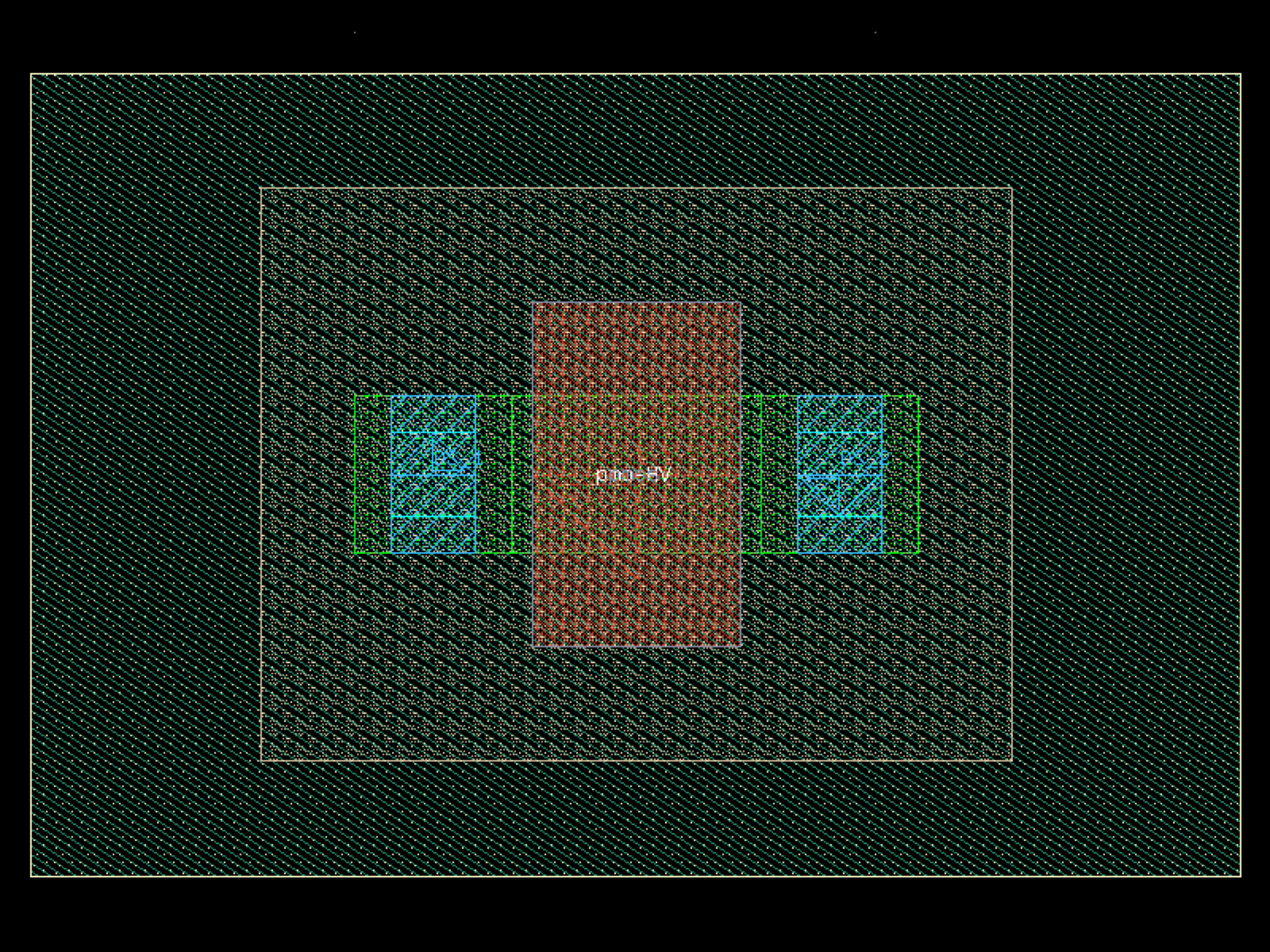
pmosHV#
- ihp.cells2.pmosHV(w=0.3, l=0.4, ng=1, guardRingType='none', guardRingDistance=1)[source]#
Create a high-voltage PMOS (PMOSHV) transistor layout.
This function generates a parametric high-voltage PMOS transistor with configurable width, length, number of gates/fingers, and optional P-substrate guard ring.
- Parameters:
w (float) – Total width of the transistor in micrometers.
l (float) – Length of the transistor in micrometers.
ng (int) – Number of gates/fingers.
guardRingType (Literal['none', 'psub']) – Type of guard ring to include. Options: - ‘none’: No guard ring. - ‘psub’: P-substrate guard ring.
guardRingDistance (float) – Spacing between the transistor and the guard ring, in micrometers.
- Returns:
The generated high-voltage PMOS transistor layout.
- Return type:
gdsfactory.Component
import warnings
warnings.filterwarnings("ignore", category=DeprecationWarning)

from ihp import PDK
from ihp import cells2

PDK.activate()

c = cells2.pmosHV(w=0.3, l=0.4, ng=1, guardRingType='none', guardRingDistance=1).copy()
c.draw_ports()
c.plot()
(Source code, png, hires.png, pdf)
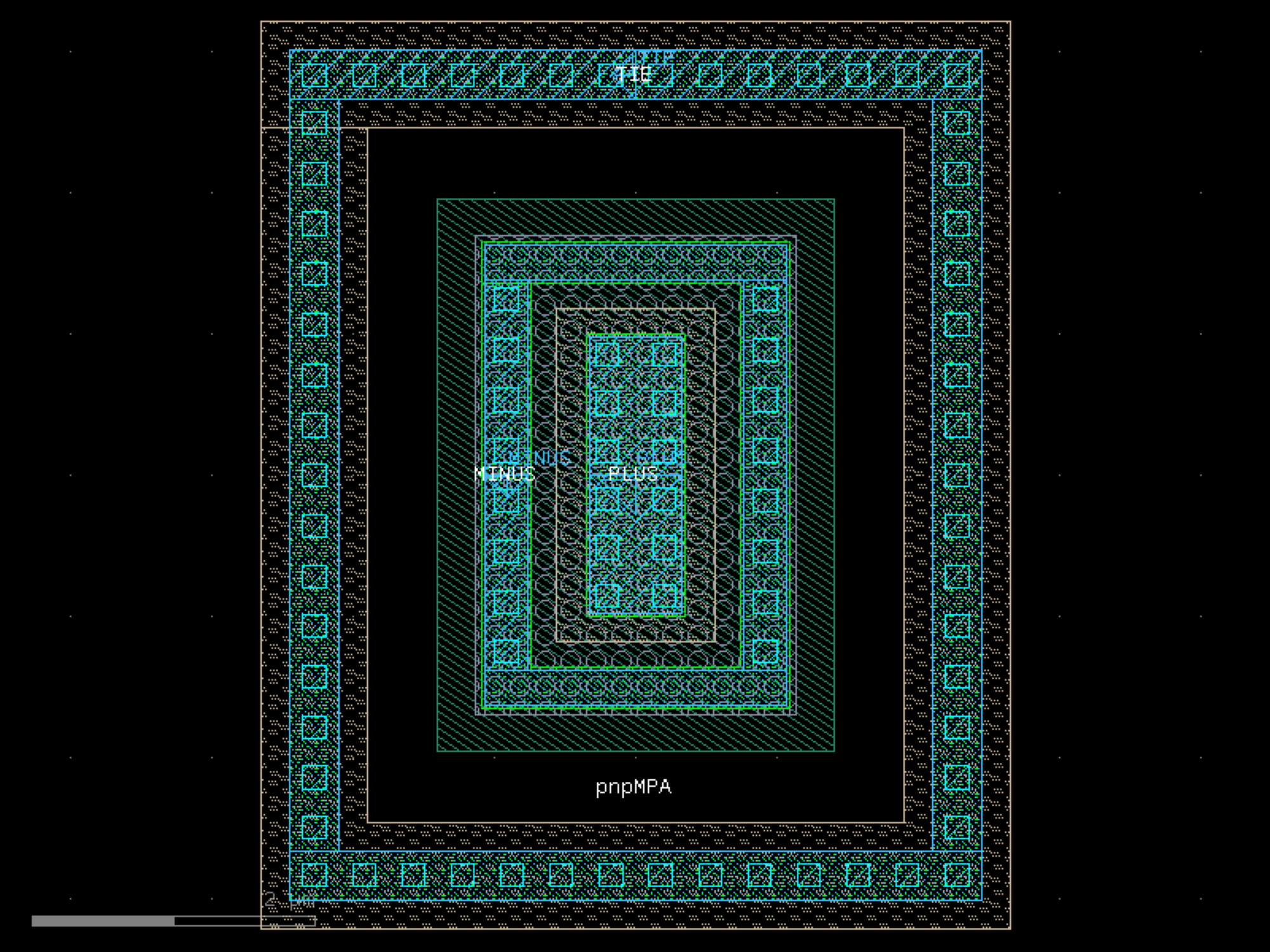
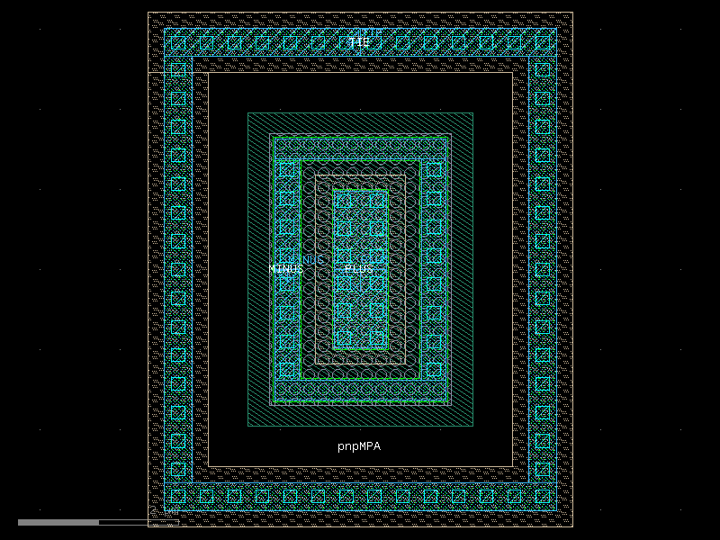
pnpMPA#
- ihp.cells2.pnpMPA(width=0.7, length=2)[source]#
Returns the IHP pnpMPA BJT transistor as a gdsfactory Component.
This function generates a layout for a PNP transistor using the IHP process. The geometry of the transistor is defined by its width and length.
- Parameters:
width (float) – Width of the transistor, in microns.
length (float) – Length of the transistor, in microns.
- Returns:
The generated pnpMPA transistor layout.
- Return type:
gdsfactory.Component
import warnings
warnings.filterwarnings("ignore", category=DeprecationWarning)

from ihp import PDK
from ihp import cells2

PDK.activate()

c = cells2.pnpMPA(width=0.7, length=2).copy()
c.draw_ports()
c.plot()
(Source code, png, hires.png, pdf)
ptap1#
- ihp.cells2.ptap1(width=0.78, length=0.78)[source]#
Create a P+ substrate tap layout.
This function generates a parametric P+ substrate tap with configurable width and length. It is typically used for connecting the P-substrate to a reference potential.
- Parameters:
width (float) – Width of the tap in micrometers.
length (float) – Length of the tap in micrometers.
- Returns:
The generated P+ substrate tap layout.
- Return type:
gdsfactory.Component
import warnings
warnings.filterwarnings("ignore", category=DeprecationWarning)

from ihp import PDK
from ihp import cells2

PDK.activate()

c = cells2.ptap1(width=0.78, length=0.78).copy()
c.draw_ports()
c.plot()
(Source code, png, hires.png, pdf)

rfcmim#
- ihp.cells2.rfcmim(width=6.99, length=6.99, feed_width=3)[source]#
Create an RF MIM (Metal-Insulator-Metal) capacitor with optimized layout.
This function generates a layout for an RF MIM capacitor with a feed line. The capacitor dimensions and feed width can be customized.
- Parameters:
width (float) – Width of the capacitor in micrometers.
length (float) – Length of the capacitor in micrometers.
feed_width (float) – Width of the feed line connecting to the capacitor, in micrometers.
- Returns:
The generated RF MIM capacitor layout.
- Return type:
gdsfactory.Component
import warnings
warnings.filterwarnings("ignore", category=DeprecationWarning)

from ihp import PDK
from ihp import cells2

PDK.activate()

c = cells2.rfcmim(width=6.99, length=6.99, feed_width=3).copy()
c.draw_ports()
c.plot()
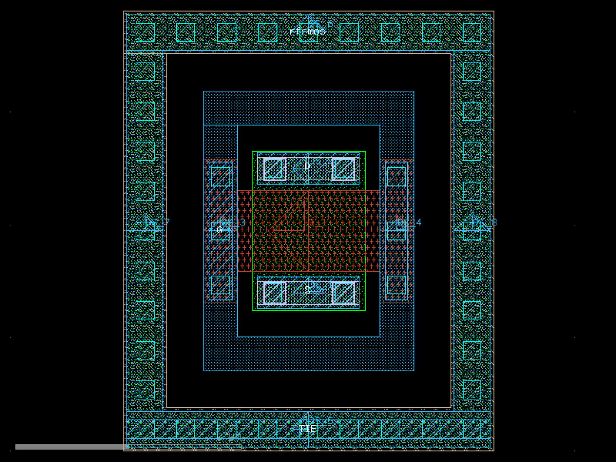
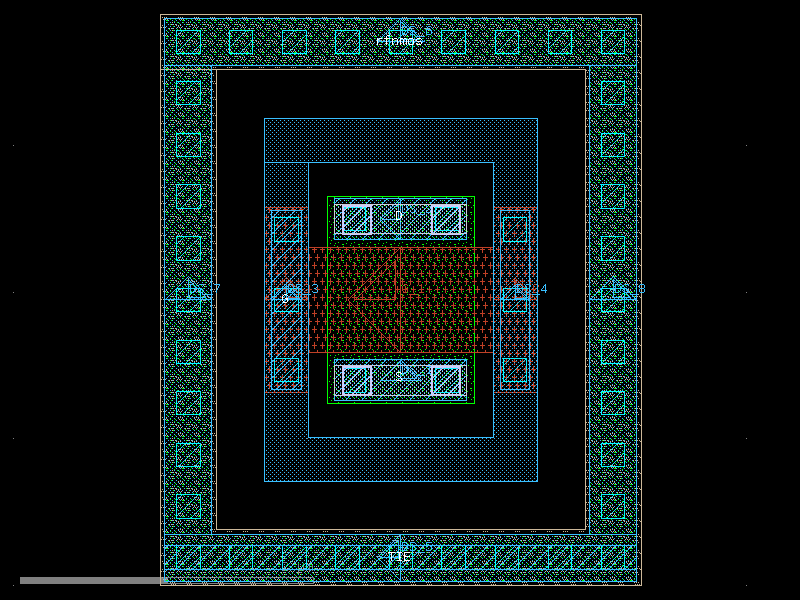
rfnmos#
- ihp.cells2.rfnmos(w=1.0, l=0.72, ng=1, cnt_rows=1, Met2Cont='Yes', gat_ring='Yes', guard_ring='Yes')[source]#
Create an RF NMOS transistor layout.
This function generates a parametric RF NMOS transistor with configurable width, length, number of gates/fingers, number of rows, and optional contacts and guard structures.
- Parameters:
w (float) – Total width of the transistor in micrometers.
l (float) – Length of the transistor in micrometers.
ng (int) – Number of gates/fingers.
cnt_rows (int) – Number of transistor rows (vertical stacking of fingers).
Met2Cont (Literal['Yes', 'No']) – Include Metal2-to-contact connection. Options: ‘Yes’ or ‘No’.
gat_ring (Literal['Yes', 'No']) – Include gate ring around the transistor. Options: ‘Yes’ or ‘No’.
guard_ring (Literal['Yes', 'No', 'U', 'Top+Bottom']) – Include guard ring around the transistor. Options: - ‘U’: U-shaped guard ring (One side stays open). - ‘Top+Bottom’: Guard ring on top and bottom (North/South). - ‘Yes’: Default guard ring. - ‘No’: No guard ring.
- Returns:
The generated RF NMOS transistor layout.
- Return type:
gdsfactory.Component
import warnings
warnings.filterwarnings("ignore", category=DeprecationWarning)

from ihp import PDK
from ihp import cells2

PDK.activate()

c = cells2.rfnmos(w=1.0, l=0.72, ng=1, cnt_rows=1, Met2Cont='Yes', gat_ring='Yes', guard_ring='Yes').copy()
c.draw_ports()
c.plot()
(Source code, png, hires.png, pdf)
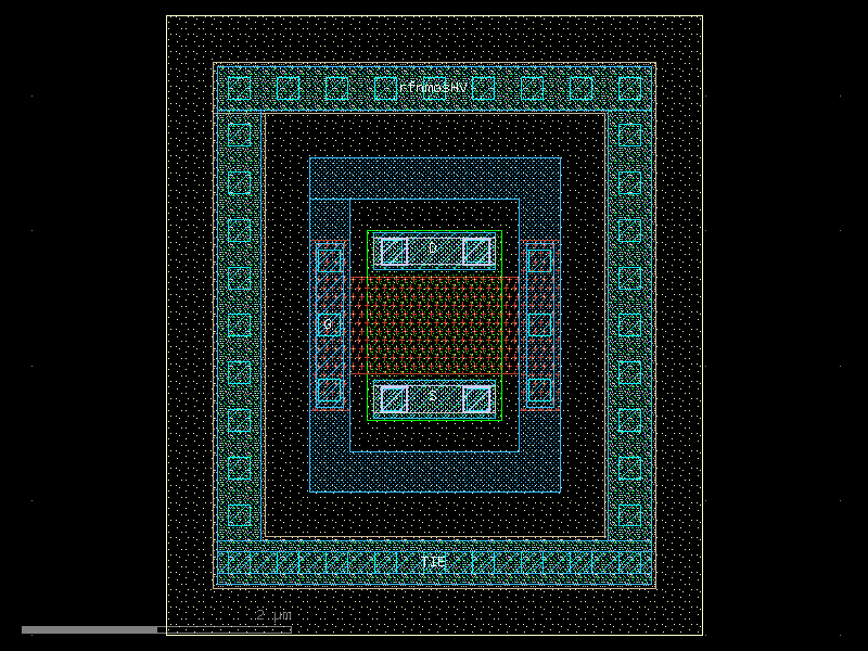
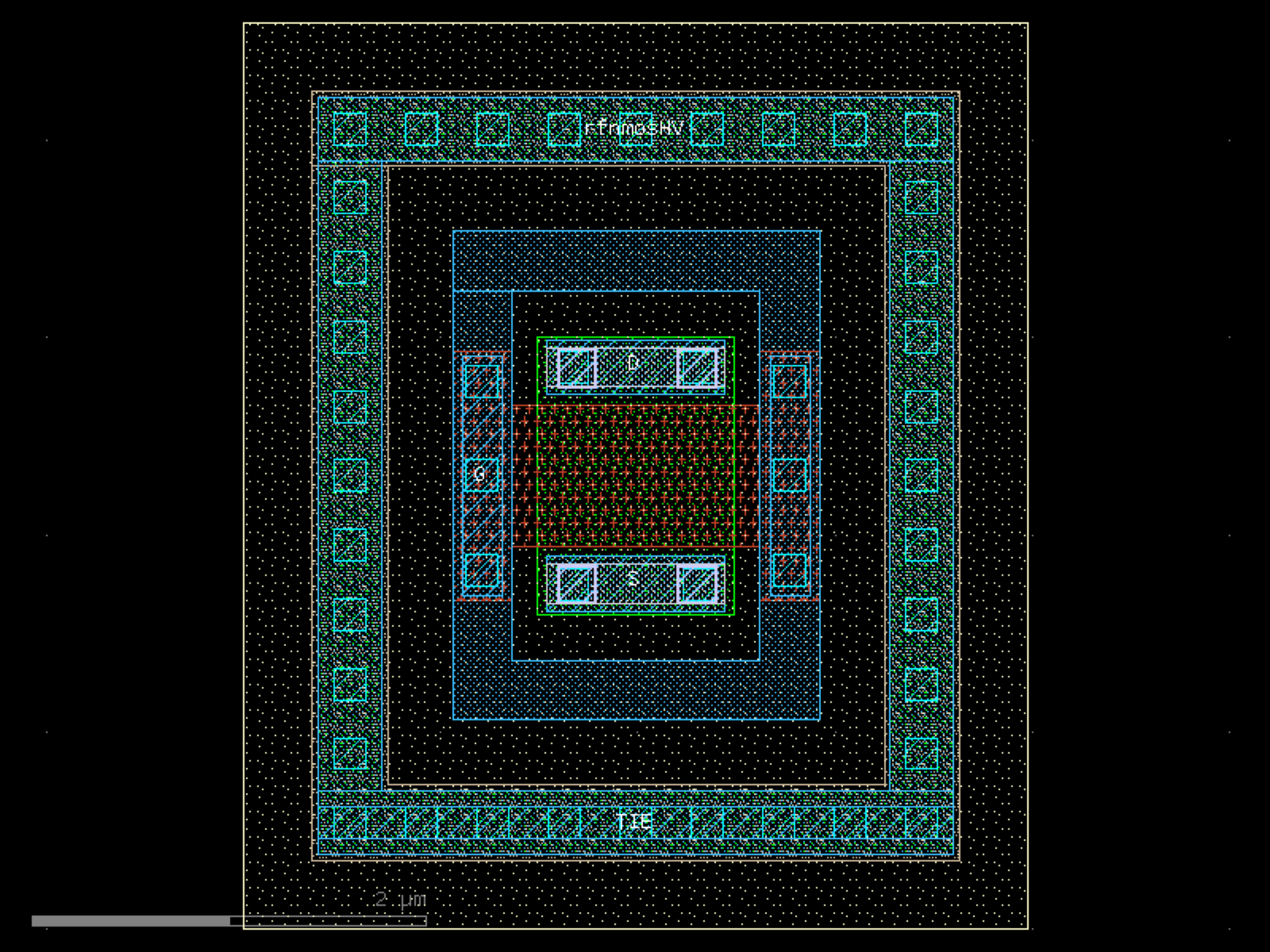
rfnmosHV#
- ihp.cells2.rfnmosHV(w=1.0, l=0.72, ng=1, cnt_rows=1, Met2Cont='Yes', gat_ring='Yes', guard_ring='Yes')[source]#
Create a high-voltage RF NMOS (rfnmosHV) transistor layout.
This function generates a parametric high-voltage RF NMOS transistor with configurable width, length, number of gates/fingers, number of rows, and optional contacts, gate ring, and guard ring structures.
- Parameters:
w (float) – Total width of the transistor in micrometers.
l (float) – Length of the transistor in micrometers.
ng (int) – Number of gates/fingers.
cnt_rows (int) – Number of transistor rows (vertical stacking of fingers).
Met2Cont (Literal['Yes', 'No']) – Include Metal2-to-contact connection. Options: ‘Yes’ or ‘No’.
gat_ring (Literal['Yes', 'No']) – Include gate ring around the transistor. Options: ‘Yes’ or ‘No’.
guard_ring (Literal['Yes', 'No', 'U', 'Top+Bottom']) – Include guard ring around the transistor. Options: - ‘U’: U-shaped guard ring (One side stays open). - ‘Top+Bottom’: Guard ring on top and bottom (North/South). - ‘Yes’: Default guard ring. - ‘No’: No guard ring.
- Returns:
The generated high-voltage RF NMOS transistor layout.
- Return type:
gdsfactory.Component
import warnings
warnings.filterwarnings("ignore", category=DeprecationWarning)

from ihp import PDK
from ihp import cells2

PDK.activate()

c = cells2.rfnmosHV(w=1.0, l=0.72, ng=1, cnt_rows=1, Met2Cont='Yes', gat_ring='Yes', guard_ring='Yes').copy()
c.draw_ports()
c.plot()
(Source code, png, hires.png, pdf)

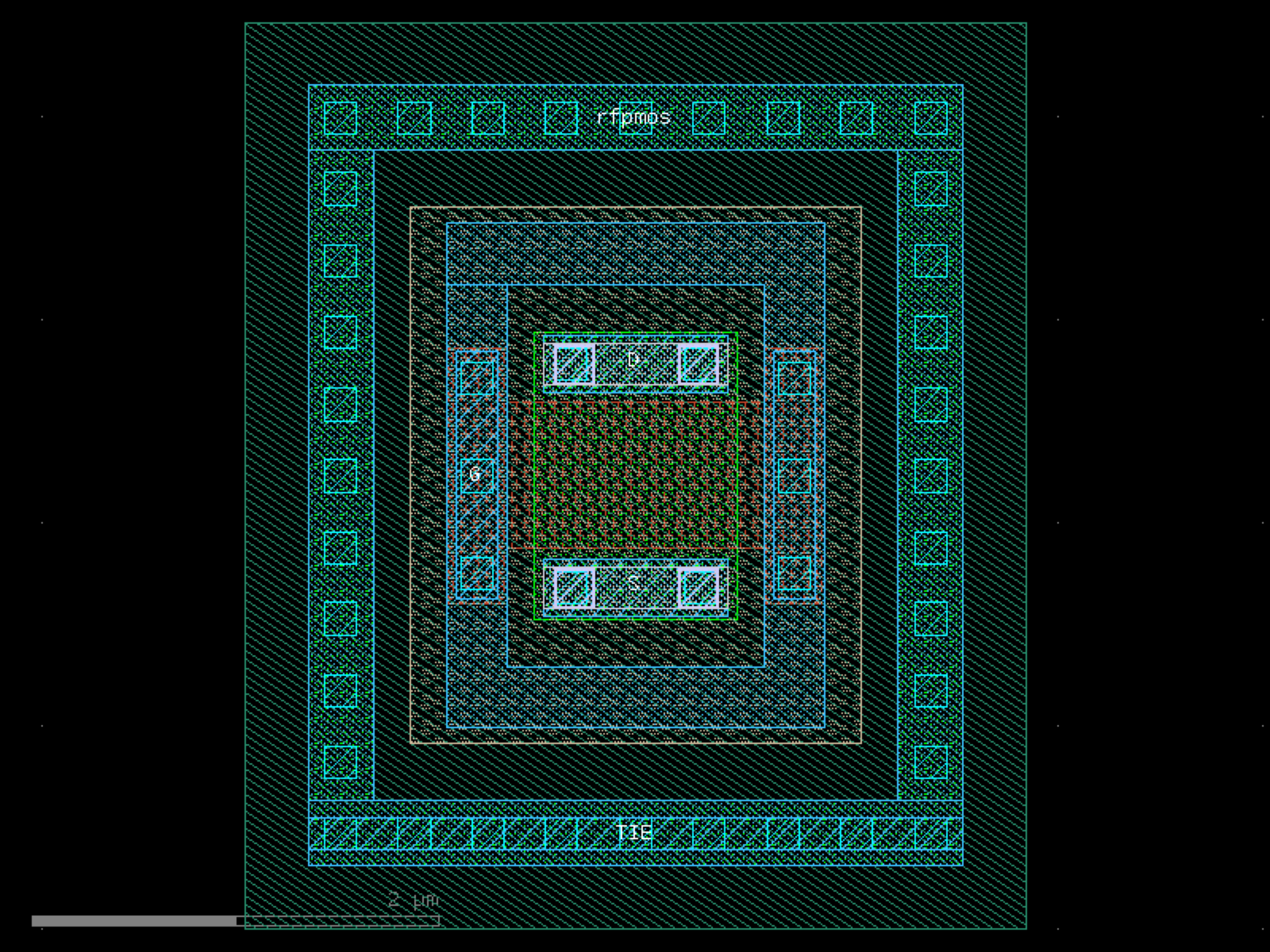
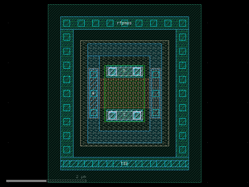
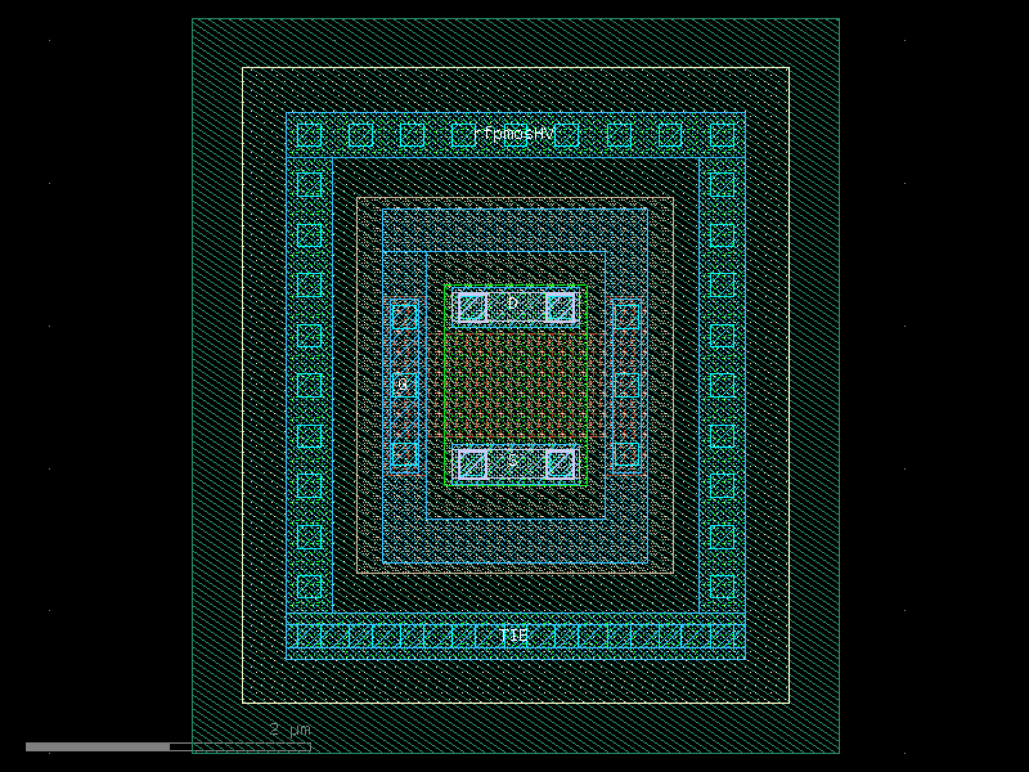
rfpmos#
- ihp.cells2.rfpmos(w=1.0, l=0.72, ng=1, cnt_rows=1, Met2Cont='Yes', gat_ring='Yes', guard_ring='Yes')[source]#
Create an RF PMOS transistor layout.
This function generates a parametric RF PMOS transistor with configurable width, length, number of gates/fingers, number of rows, and optional contacts, gate ring, and guard ring structures.
- Parameters:
w (float) – Total width of the transistor in micrometers.
l (float) – Length of the transistor in micrometers.
ng (int) – Number of gates/fingers.
cnt_rows (int) – Number of transistor rows (vertical stacking of fingers).
Met2Cont (Literal['Yes', 'No']) – Include Metal2-to-contact connection. Options: ‘Yes’ or ‘No’.
gat_ring (Literal['Yes', 'No']) – Include gate ring around the transistor. Options: ‘Yes’ or ‘No’.
guard_ring (Literal['Yes', 'No', 'U', 'Top+Bottom']) – Include guard ring around the transistor. Options: - ‘U’: U-shaped guard ring (One side stays open). - ‘Top+Bottom’: Guard ring on top and bottom (North/South). - ‘Yes’: Default guard ring. - ‘No’: No guard ring.
- Returns:
The generated RF PMOS transistor layout.
- Return type:
gdsfactory.Component
import warnings
warnings.filterwarnings("ignore", category=DeprecationWarning)

from ihp import PDK
from ihp import cells2

PDK.activate()

c = cells2.rfpmos(w=1.0, l=0.72, ng=1, cnt_rows=1, Met2Cont='Yes', gat_ring='Yes', guard_ring='Yes').copy()
c.draw_ports()
c.plot()
(Source code, png, hires.png, pdf)
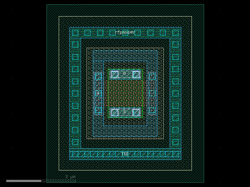
rfpmosHV#
- ihp.cells2.rfpmosHV(w=1.0, l=0.72, ng=1, cnt_rows=1, Met2Cont='Yes', gat_ring='Yes', guard_ring='Yes')[source]#
Create a high-voltage RF PMOS (rfpmosHV) transistor layout.
This function generates a parametric high-voltage RF PMOS transistor with configurable width, length, number of gates/fingers, number of rows, and optional contacts, gate ring, and guard ring structures.
- Parameters:
w (float) – Total width of the transistor in micrometers.
l (float) – Length of the transistor in micrometers.
ng (int) – Number of gates/fingers.
cnt_rows (int) – Number of transistor rows (vertical stacking of fingers).
Met2Cont (Literal['Yes', 'No']) – Include Metal2-to-contact connection. Options: ‘Yes’ or ‘No’.
gat_ring (Literal['Yes', 'No']) – Include gate ring around the transistor. Options: ‘Yes’ or ‘No’.
guard_ring (Literal['Yes', 'No', 'U', 'Top+Bottom']) – Include guard ring around the transistor. Options: - ‘U’: U-shaped guard ring (One side stays open). - ‘Top+Bottom’: Guard ring on top and bottom (North/South). - ‘Yes’: Default guard ring. - ‘No’: No guard ring.
- Returns:
The generated high-voltage RF PMOS transistor layout.
- Return type:
gdsfactory.Component
import warnings
warnings.filterwarnings("ignore", category=DeprecationWarning)

from ihp import PDK
from ihp import cells2

PDK.activate()

c = cells2.rfpmosHV(w=1.0, l=0.72, ng=1, cnt_rows=1, Met2Cont='Yes', gat_ring='Yes', guard_ring='Yes').copy()
c.draw_ports()
c.plot()
(Source code, png, hires.png, pdf)

rhigh#
- ihp.cells2.rhigh(length=0.96, width=0.5, bends=0, polySpace=0.18, numberOfSegments=1, segmentConnection='Serial', segmentSpacing=2, guardRingType='none', guardRingDistance=1)[source]#
Create a high-resistance polysilicon resistor layout.
This function generates a parametric high-resistance polysilicon resistor with configurable width, length, bends, and multiple segments. Optional guard rings can be added for isolation.
- Parameters:
length (float) – Length of the resistor in micrometers.
width (float) – Width of the resistor in micrometers.
bends (int) – Number of bends in the resistor path.
polySpace (float) – Spacing between polysilicon lines in micrometers.
numberOfSegments (int) – Number of resistor segments.
segmentConnection (Literal['None', 'Serial', 'Parallel']) – Connection type between segments. Options: - ‘None’: Segments not connected. - ‘Serial’: Segments connected in series. - ‘Parallel’: Segments connected in parallel.
segmentSpacing (float) – Spacing between segments in micrometers.
guardRingType (Literal['none', 'nwell', 'psub']) – Type of guard ring to include. Options: - ‘none’: No guard ring. - ‘nwell’: N-well guard ring. - ‘psub’: P-substrate guard ring.
guardRingDistance (float) – Distance between the resistor and guard ring in micrometers.
- Returns:
The generated high-resistance polysilicon resistor layout.
- Return type:
gdsfactory.Component
import warnings
warnings.filterwarnings("ignore", category=DeprecationWarning)

from ihp import PDK
from ihp import cells2

PDK.activate()

c = cells2.rhigh(length=0.96, width=0.5, bends=0, polySpace=0.18, numberOfSegments=1, segmentConnection='Serial', segmentSpacing=2, guardRingType='none', guardRingDistance=1).copy()
c.draw_ports()
c.plot()
(Source code, png, hires.png, pdf)

rppd#
- ihp.cells2.rppd(length=0.5, width=0.5, bends=0, polySpace=0.18, numberOfSegments=1, segmentConnection='Serial', segmentSpacing=2, guardRingType='none', guardRingDistance=1)[source]#
Create a high-resistance polysilicon resistor layout.
This function generates a parametric high-resistance polysilicon resistor with configurable width, length, bends, and multiple segments. Optional guard rings can be added for isolation.
- Parameters:
length (float) – Length of the resistor in micrometers.
width (float) – Width of the resistor in micrometers.
bends (int) – Number of bends in the resistor path.
polySpace (float) – Spacing between polysilicon lines in micrometers.
numberOfSegments (int) – Number of resistor segments.
segmentConnection (Literal['None', 'Serial', 'Parallel']) – Connection type between segments. Options: - ‘None’: Segments not connected. - ‘Serial’: Segments connected in series. - ‘Parallel’: Segments connected in parallel.
segmentSpacing (float) – Spacing between segments in micrometers.
guardRingType (Literal['none', 'nwell', 'psub']) – Type of guard ring to include. Options: - ‘none’: No guard ring. - ‘nwell’: N-well guard ring. - ‘psub’: P-substrate guard ring.
guardRingDistance (float) – Distance between the resistor and guard ring in micrometers.
- Returns:
The generated high-resistance polysilicon resistor layout.
- Return type:
gdsfactory.Component
import warnings
warnings.filterwarnings("ignore", category=DeprecationWarning)

from ihp import PDK
from ihp import cells2

PDK.activate()

c = cells2.rppd(length=0.5, width=0.5, bends=0, polySpace=0.18, numberOfSegments=1, segmentConnection='Serial', segmentSpacing=2, guardRingType='none', guardRingDistance=1).copy()
c.draw_ports()
c.plot()
(Source code, png, hires.png, pdf)

rsil#
- ihp.cells2.rsil(length=0.5, width=0.5, polySpace=0.18, resistance=24.9, numberOfSegments=1, segmentConnection='Serial', segmentSpacing=2, guardRingType='none', guardRingDistance=1)[source]#
Create a high-resistance polysilicon resistor layout (RSIL type).
This function generates a parametric high-resistance polysilicon resistor of RSIL type with configurable width, length, target resistance, bends, multiple segments, and optional guard rings for isolation.
- Parameters:
length (float) – Length of the resistor in micrometers.
width (float) – Width of the resistor in micrometers.
polySpace (float) – Spacing between polysilicon lines in micrometers.
resistance (float) – Target resistance value in ohms.
numberOfSegments (int) – Number of resistor segments.
segmentConnection (Literal['None', 'Serial', 'Parallel']) – Connection type between segments. Options: - ‘None’: Segments not connected. - ‘Serial’: Segments connected in series. - ‘Parallel’: Segments connected in parallel.
segmentSpacing (float) – Spacing between segments in micrometers.
guardRingType (Literal['none', 'nwell', 'psub']) – Type of guard ring to include. Options: - ‘none’: No guard ring. - ‘nwell’: N-well guard ring. - ‘psub’: P-substrate guard ring.
guardRingDistance (float) – Distance between the resistor and guard ring in micrometers.
- Returns:
The generated RSIL polysilicon resistor layout.
- Return type:
gdsfactory.Component
import warnings
warnings.filterwarnings("ignore", category=DeprecationWarning)

from ihp import PDK
from ihp import cells2

PDK.activate()

c = cells2.rsil(length=0.5, width=0.5, polySpace=0.18, resistance=24.9, numberOfSegments=1, segmentConnection='Serial', segmentSpacing=2, guardRingType='none', guardRingDistance=1).copy()
c.draw_ports()
c.plot()
(Source code, png, hires.png, pdf)

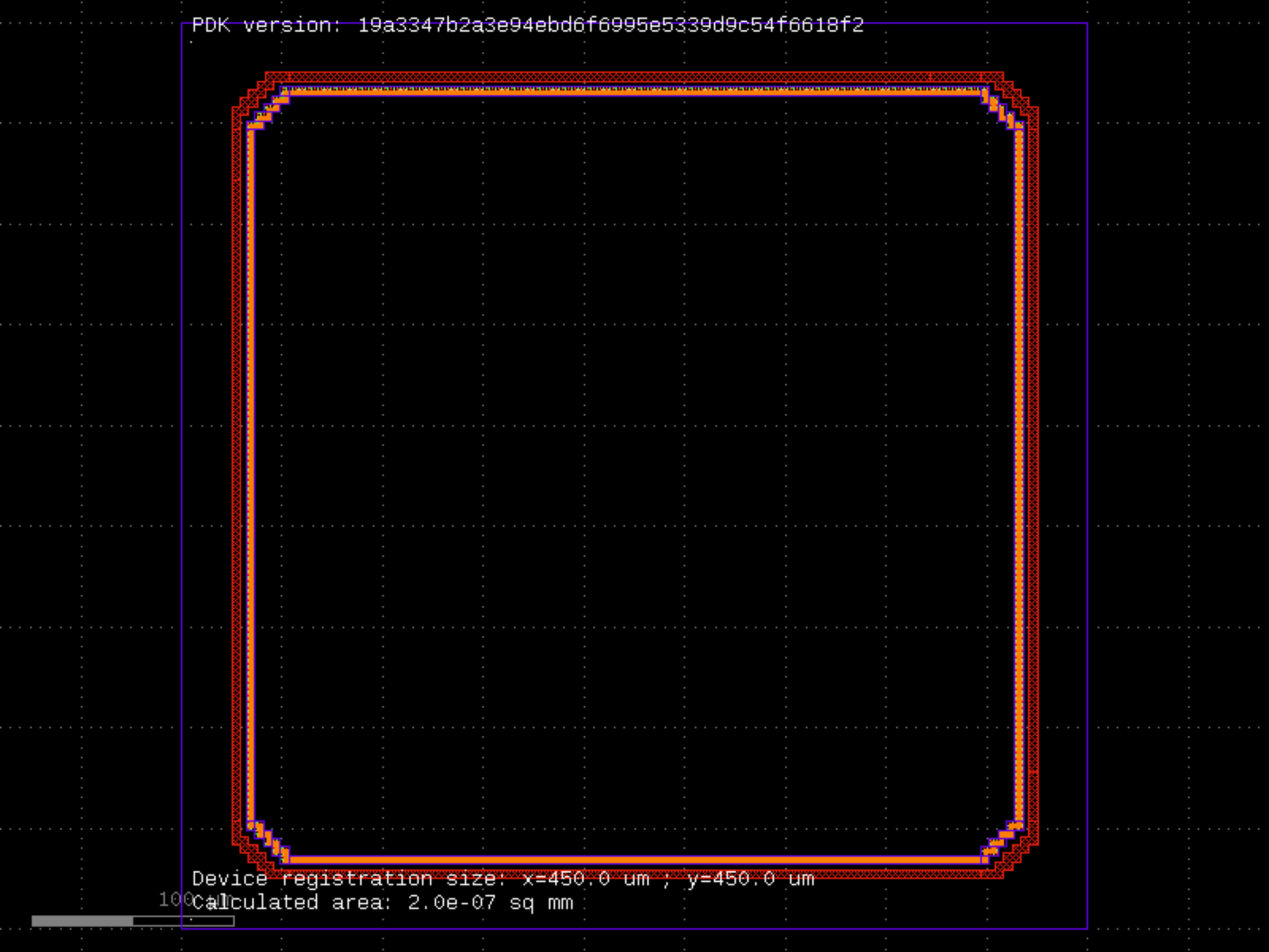
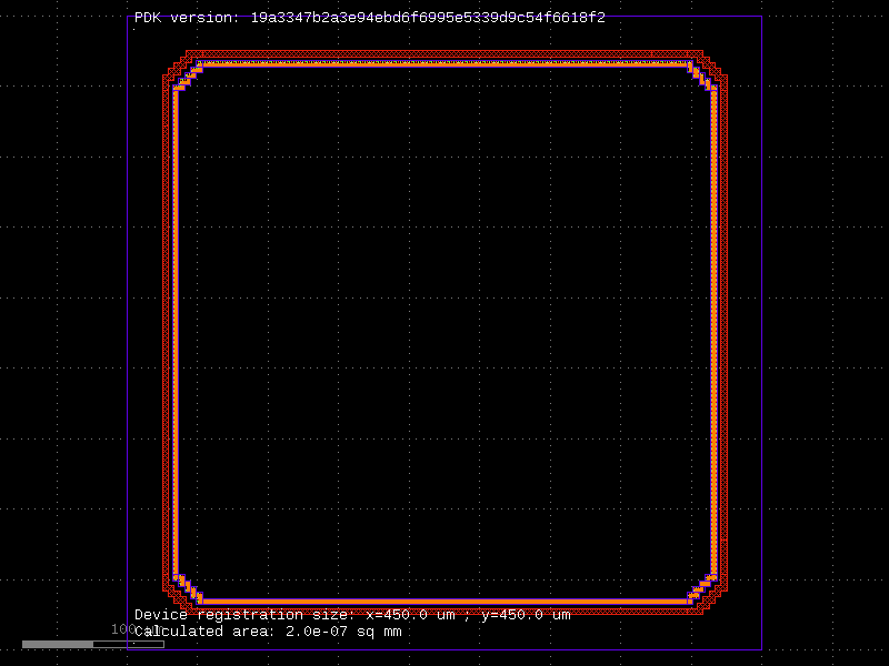
sealring#
- ihp.cells2.sealring(width=400.0, height=400.0, addLabel='nil', addSlit='nil', edgeBox=25.0)[source]#
Create a seal ring for die protection.
This function generates a parametric seal ring around the die with optional label and slit features. The seal ring helps protect the chip from mechanical stress and contamination.
- Parameters:
width (float) – Inner width of the seal ring in micrometers.
height (float) – Inner height of the seal ring in micrometers.
addLabel (Literal['nil', 't']) – Include label on the seal ring. Options: ‘nil’ (no label), ‘t’ (add label).
addSlit (Literal['nil', 't']) – Include slit in the seal ring. Options: ‘nil’ (no slit), ‘t’ (add slit).
edgeBox (float) – Distance from die edge to the seal ring in micrometers.
- Returns:
The generated seal ring layout.
- Return type:
gdsfactory.Component
import warnings
warnings.filterwarnings("ignore", category=DeprecationWarning)

from ihp import PDK
from ihp import cells2

PDK.activate()

c = cells2.sealring(width=400.0, height=400.0, addLabel='nil', addSlit='nil', edgeBox=25.0).copy()
c.draw_ports()
c.plot()
(Source code, png, hires.png, pdf)
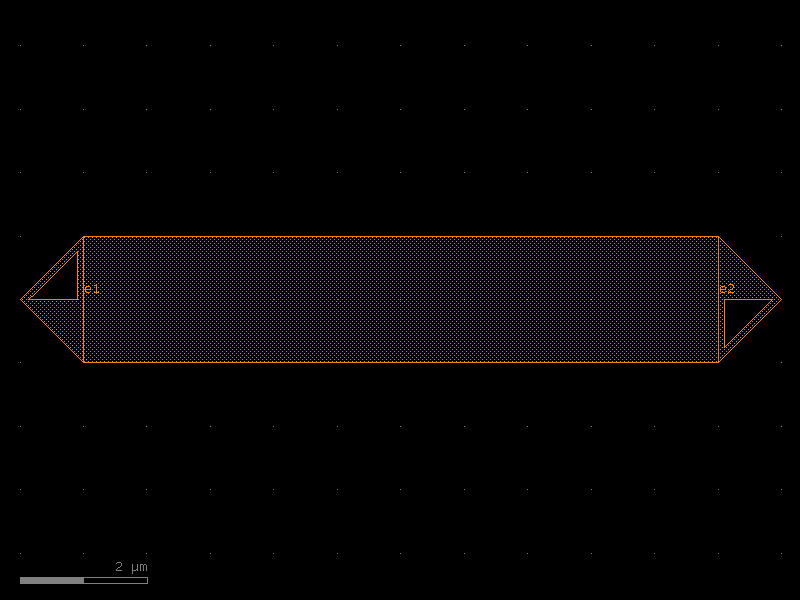
straight#
- ihp.cells2.straight(length=10, cross_section='strip', width=None, npoints=2)[source]#
Returns a Straight waveguide.
- Parameters:
length (float) – straight length (um).
cross_section (CrossSection | str | dict[str, Any] | Callable[[...], CrossSection] | SymmetricalCrossSection | DCrossSection) – specification (CrossSection, string or dict).
width (float | None) – width of the waveguide. If None, it will use the width of the cross_section.
npoints (int) – number of points.
- Return type:
Component
import warnings
warnings.filterwarnings("ignore", category=DeprecationWarning)

from ihp import PDK
from ihp import cells2

PDK.activate()

c = cells2.straight(length=10, cross_section='strip', npoints=2).copy()
c.draw_ports()
c.plot()
(Source code, png, hires.png, pdf)

straight_metal#
- ihp.cells2.straight_metal(length=10, cross_section='metal_routing', width=None)[source]#
Returns a Straight waveguide.
- Parameters:
length (float) – straight length (um).
cross_section (CrossSection | str | dict[str, Any] | Callable[[...], CrossSection] | SymmetricalCrossSection | DCrossSection) – specification (CrossSection, string or dict).
width (float | None) – width of the waveguide. If None, it will use the width of the cross_section.
- Return type:
Component
import warnings
warnings.filterwarnings("ignore", category=DeprecationWarning)

from ihp import PDK
from ihp import cells2

PDK.activate()

c = cells2.straight_metal(length=10, cross_section='metal_routing').copy()
c.draw_ports()
c.plot()
(Source code, png, hires.png, pdf)

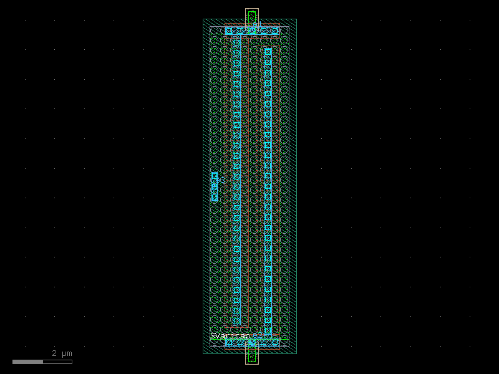
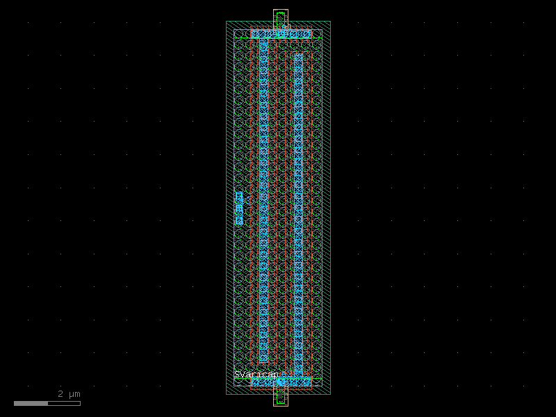
svaricap#
- ihp.cells2.svaricap(width='9.74u', length='0.8u', Nx=1, guardRingType='none', guardRingDistance=1)[source]#
Create a MOS varicap (variable capacitor) layout.
This function generates a parametric MOS varicap with optional n-well guard rings. The device geometry and number of fingers can be customized.
- Parameters:
width (Literal['3.74u', '9.74u']) – Width of the varicap. Must be one of: ‘3.74u’, ‘9.74u’.
length (Literal['0.3u', '0.8u']) – Length of the varicap. Must be one of: ‘0.3u’, ‘0.8u’.
Nx (int) – Number of fingers for the varicap.
guardRingType (Literal['none', 'nwell']) – Type of guard ring to include. Options: - ‘none’: No guard ring. - ‘nwell’: N-well guard ring.
guardRingDistance (float) – Spacing between the varicap body and the guard ring, in micrometers.
- Returns:
The generated varicap layout.
- Return type:
gdsfactory.Component
import warnings
warnings.filterwarnings("ignore", category=DeprecationWarning)

from ihp import PDK
from ihp import cells2

PDK.activate()

c = cells2.svaricap(width='9.74u', length='0.8u', Nx=1, guardRingType='none', guardRingDistance=1).copy()
c.draw_ports()
c.plot()
(Source code, png, hires.png, pdf)
text_rectangular#
- ihp.cells2.text_rectangular(text='abc', size=3, justify='left', layer='TOPMETAL2')[source]#
Pixel based font, guaranteed to be manhattan, without acute angles.
- Parameters:
text (str) – string.
size (float) – pixel size.
justify (str) – left, right or center.
layer (tuple[int, int] | str | int | LayerEnum) – for text.
- Return type:
Component
import warnings
warnings.filterwarnings("ignore", category=DeprecationWarning)

from ihp import PDK
from ihp import cells2

PDK.activate()

c = cells2.text_rectangular(text='abc', size=3, justify='left', layer='TOPMETAL2').copy()
c.draw_ports()
c.plot()
text_rectangular_multi_layer#
- ihp.cells2.text_rectangular_multi_layer(text='abc', layers=('TOPMETAL2',), text_factory='text_rectangular', **kwargs)[source]#
Returns rectangular text in different layers.
- Parameters:
text (str) – string of text.
layers (Sequence[tuple[int, int] | str | int | LayerEnum]) – list of layers to replicate the text.
text_factory (str | Callable[[...], Component] | dict[str, Any] | DKCell | partial[Component]) – function to create the text Components.
kwargs (Any) – keyword arguments for text_factory.
- Return type:
Component
import warnings
warnings.filterwarnings("ignore", category=DeprecationWarning)

from ihp import PDK
from ihp import cells2

PDK.activate()

c = cells2.text_rectangular_multi_layer(text='abc', layers=('TOPMETAL2',), text_factory='text_rectangular').copy()
c.draw_ports()
c.plot()
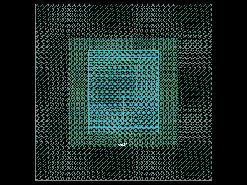
via_stack#
- ihp.cells2.via_stack(bottom_layer='Metal1', top_layer='Metal2', vn_columns=2, vn_rows=2, vt1_columns=1, vt1_rows=1, vt2_columns=1, vt2_rows=1)[source]#
Create a via stack component.
This function generates a layout for a via stack connecting a bottom layer to a top layer. The number of columns and rows for standard vias (Via1-Via4) and top vias (TopVia1, TopVia2) can be specified.
- Parameters:
bottom_layer (Literal['Activ', 'GatPoly', 'Metal1', 'Metal2', 'Metal3', 'Metal4', 'Metal5', 'TopMetal1', 'TopMetal2']) – Bottom layer name. Options: ‘Activ’, ‘GatPoly’, ‘Metal1’-‘Metal5’, ‘TopMetal1’, ‘TopMetal2’.
top_layer (Literal['Activ', 'GatPoly', 'Metal1', 'Metal2', 'Metal3', 'Metal4', 'Metal5', 'TopMetal1', 'TopMetal2']) – Top layer name. Options: ‘Activ’, ‘GatPoly’, ‘Metal1’-‘Metal5’, ‘TopMetal1’, ‘TopMetal2’.
vn_columns (int) – Number of columns for standard vias (Via1-Via4).
vn_rows (int) – Number of rows for standard vias.
vt1_columns (int) – Number of columns for TopVia1.
vt1_rows (int) – Number of rows for TopVia1.
vt2_columns (int) – Number of columns for TopVia2.
vt2_rows (int) – Number of rows for TopVia2.
- Returns:
The generated via stack test layout.
- Return type:
gdsfactory.Component
import warnings
warnings.filterwarnings("ignore", category=DeprecationWarning)

from ihp import PDK
from ihp import cells2

PDK.activate()

c = cells2.via_stack(bottom_layer='Metal1', top_layer='Metal2', vn_columns=2, vn_rows=2, vt1_columns=1, vt1_rows=1, vt2_columns=1, vt2_rows=1).copy()
c.draw_ports()
c.plot()
(Source code, png, hires.png, pdf)

wire_corner#
- ihp.cells2.wire_corner(cross_section='metal_routing', width=None)[source]#
Returns 45 degrees electrical corner wire.
- Parameters:
cross_section (CrossSection | str | dict[str, Any] | Callable[[...], CrossSection] | SymmetricalCrossSection | DCrossSection) – spec.
width (float | None) – optional width. Defaults to cross_section width.
- Return type:
Component
import warnings
warnings.filterwarnings("ignore", category=DeprecationWarning)

from ihp import PDK
from ihp import cells2

PDK.activate()

c = cells2.wire_corner(cross_section='metal_routing').copy()
c.draw_ports()
c.plot()
(Source code, png, hires.png, pdf)

wire_corner45#
- ihp.cells2.wire_corner45(cross_section='metal_routing', radius=10, width=None, layer=None, with_corner90_ports=True)[source]#
Returns 90 degrees electrical corner wire.
- Parameters:
cross_section (CrossSection | str | dict[str, Any] | Callable[[...], CrossSection] | SymmetricalCrossSection | DCrossSection) – spec.
radius (float) – ignored.
width (float | None) – optional width. Defaults to cross_section width.
layer (tuple[int, int] | str | int | LayerEnum | None) – ignored.
with_corner90_ports (bool) – if True, adds ports at 90 degrees.
- Return type:
Component
import warnings
warnings.filterwarnings("ignore", category=DeprecationWarning)

from ihp import PDK
from ihp import cells2

PDK.activate()

c = cells2.wire_corner45(cross_section='metal_routing', radius=10, with_corner90_ports=True).copy()
c.draw_ports()
c.plot()
(Source code, png, hires.png, pdf)