Cells Ge-on-Si
array
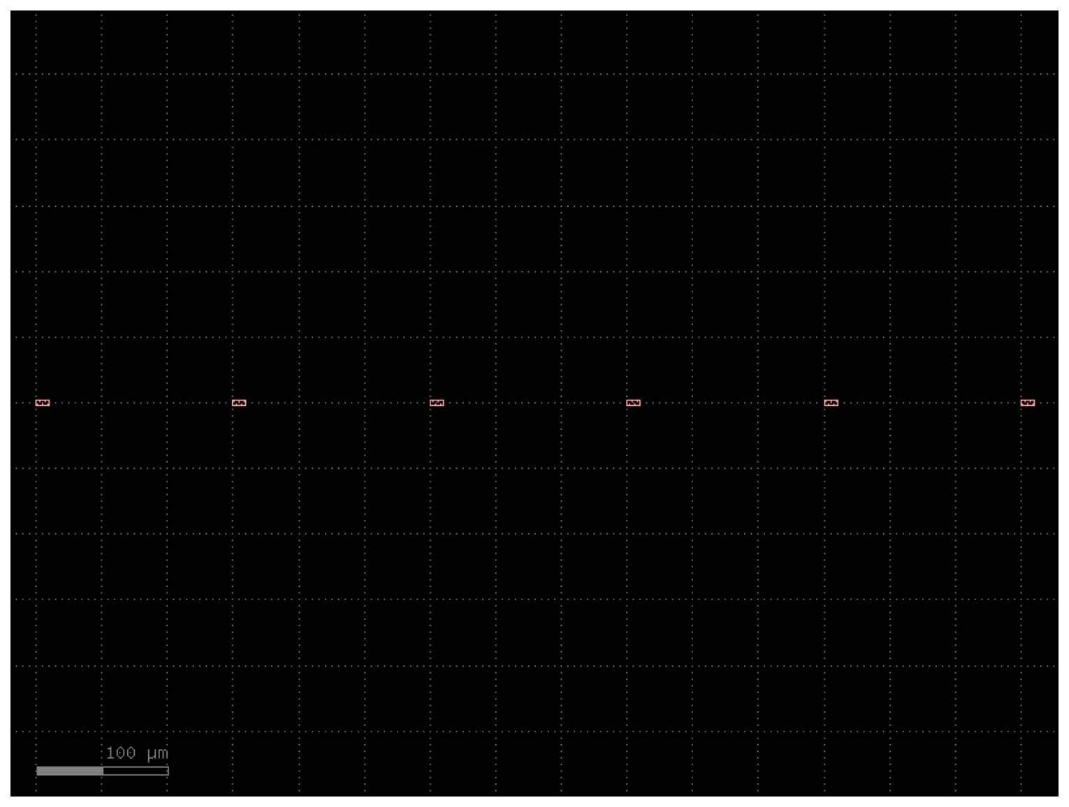
An array of components.
Parameters:
| Name | Type | Description | Default |
|---|---|---|---|
component
|
ComponentSpec
|
the component of which to create an array. |
partial(straight, cross_section='xs_rib')
|
columns
|
int
|
the number of components to place in the x-direction. |
6
|
rows
|
int
|
the number of components to place in the y-direction. |
1
|
add_ports
|
bool
|
add ports to the component. |
True
|
size
|
Optional x, y size. Overrides columns and rows. |
None
|
|
centered
|
bool
|
center the array around the origin. |
False
|
column_pitch
|
float
|
the pitch between columns. |
150
|
row_pitch
|
float
|
the pitch between rows. |
150
|
:noindex:
from cspdk.ge_on_si import cells, PDK

PDK.activate()

c = cells.array(columns=6, rows=1, add_ports=True, centered=False, column_pitch=150, row_pitch=150)
c.draw_ports()
c.plot()
bend_circular
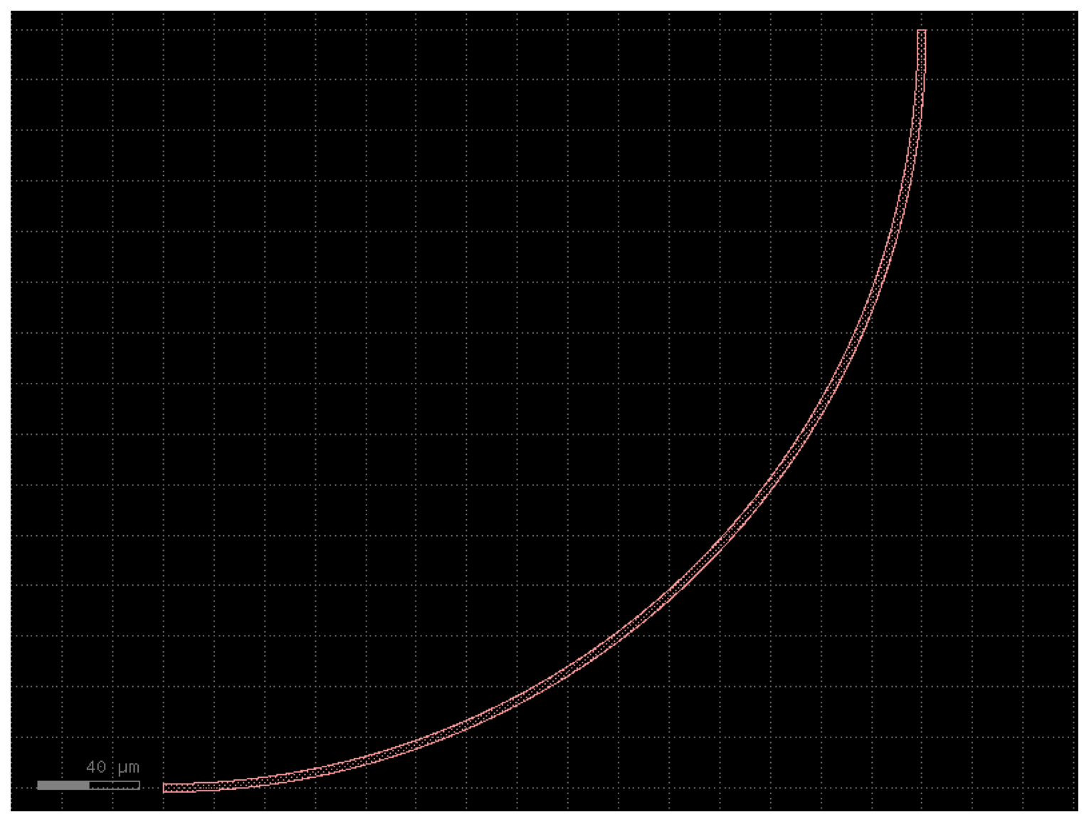
A circular bend, matching the foundry reference bend geometry.
The Ge_on_Si_3800nm_TE_RIB_90_Degree_Bend reference GDS is a circular arc with a 300 um center-line radius (the xs_rib default). This is the routing bend of the PDK.
Parameters:
| Name | Type | Description | Default |
|---|---|---|---|
radius
|
float | None
|
the radius of the bend (defaults to the cross-section radius). |
None
|
angle
|
float
|
the angle of the bend (usually 90 degrees). |
90.0
|
width
|
float | None
|
the width of the waveguide forming the bend. |
None
|
cross_section
|
CrossSectionSpec
|
a cross section or its name or a function generating a cross section. |
'xs_rib'
|
:noindex:
from cspdk.ge_on_si import cells, PDK

PDK.activate()

c = cells.bend_circular(angle=90, cross_section='xs_rib')
c.draw_ports()
c.plot()
bend_euler
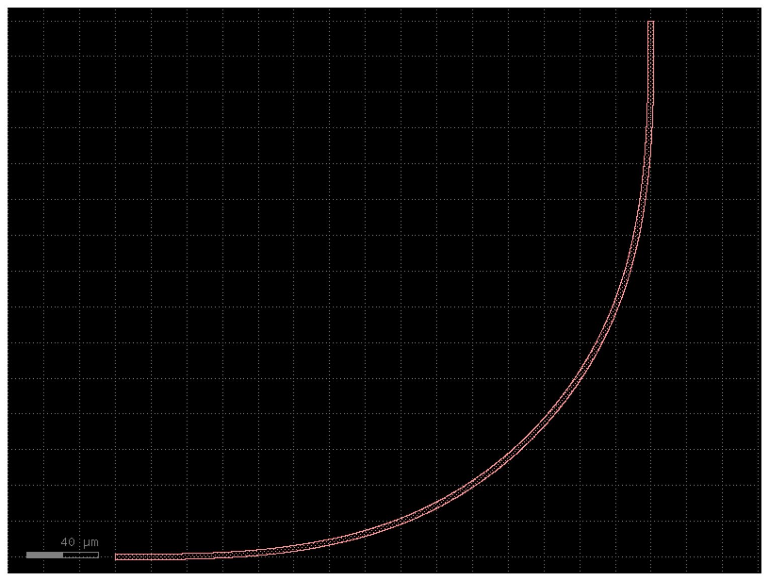
An euler bend.
Parameters:
| Name | Type | Description | Default |
|---|---|---|---|
radius
|
float | None
|
the effective radius of the bend. |
None
|
angle
|
float
|
the angle of the bend (usually 90 degrees). |
90.0
|
p
|
float
|
the fraction of the bend that's represented by a polar bend. |
0.5
|
width
|
float | None
|
the width of the waveguide forming the bend. |
None
|
cross_section
|
CrossSectionSpec
|
a cross section or its name or a function generating a cross section. |
'xs_rib'
|
:noindex:
from cspdk.ge_on_si import cells, PDK

PDK.activate()

c = cells.bend_euler(angle=90, p=0.5, cross_section='xs_rib')
c.draw_ports()
c.plot()
bend_s
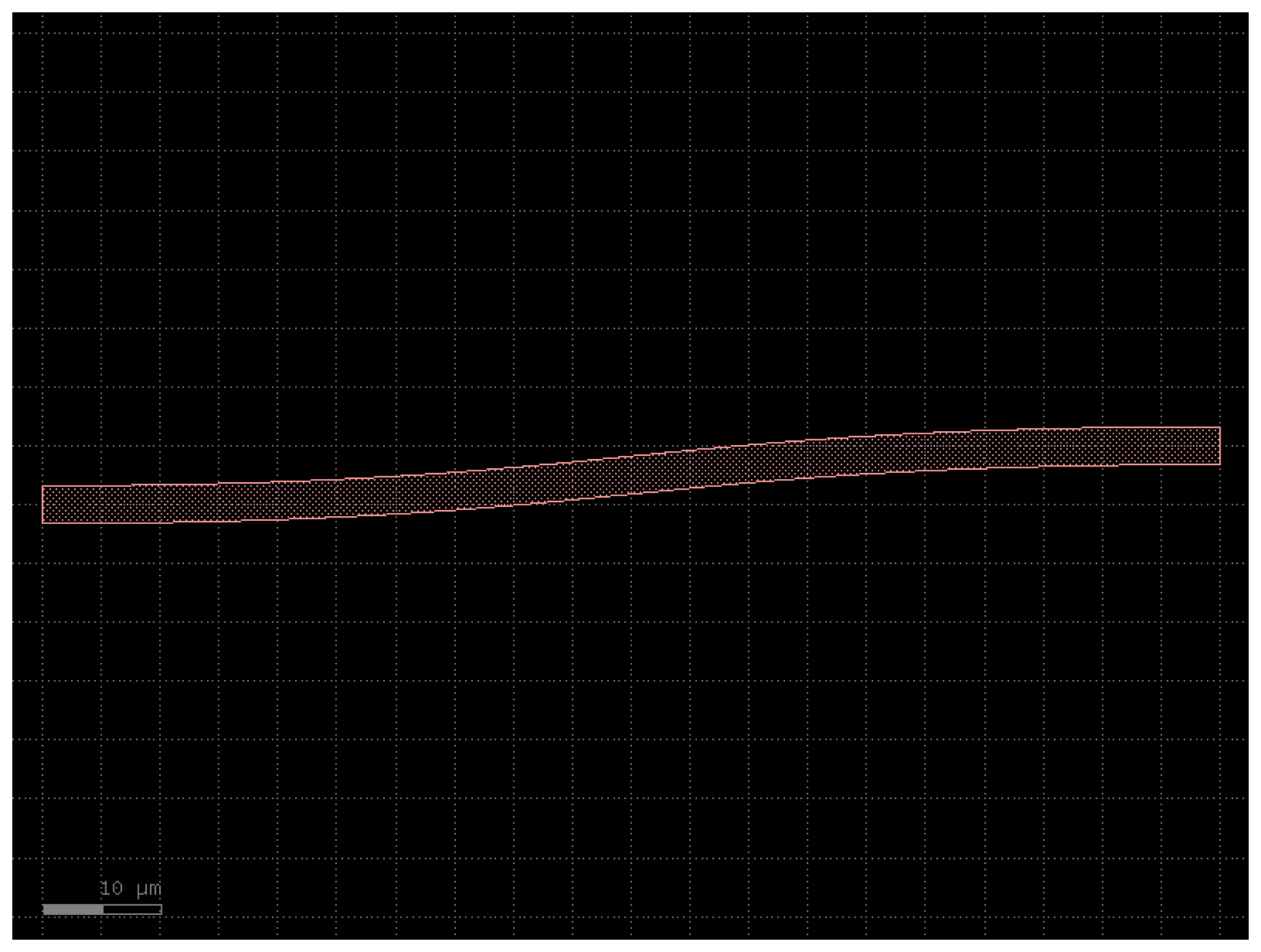
An S-bend.
The default size keeps the minimum bend radius (~365 um) above the 300 um rib minimum; (80, 5) dipped to ~234 um.
Parameters:
| Name | Type | Description | Default |
|---|---|---|---|
size
|
tuple[float, float]
|
the width and height of the s-bend. |
(100.0, 5.0)
|
cross_section
|
CrossSectionSpec
|
a cross section or its name or a function generating a cross section. |
'xs_rib'
|
allow_min_radius_violation
|
bool
|
if True, allows the s-bend to have a smaller radius than the minimum radius. |
True
|
width
|
float | None
|
waveguide width; defaults to the cross-section width. |
None
|
:noindex:
from cspdk.ge_on_si import cells, PDK

PDK.activate()

c = cells.bend_s(size=(100, 5), cross_section='xs_rib', allow_min_radius_violation=True)
c.draw_ports()
c.plot()
die
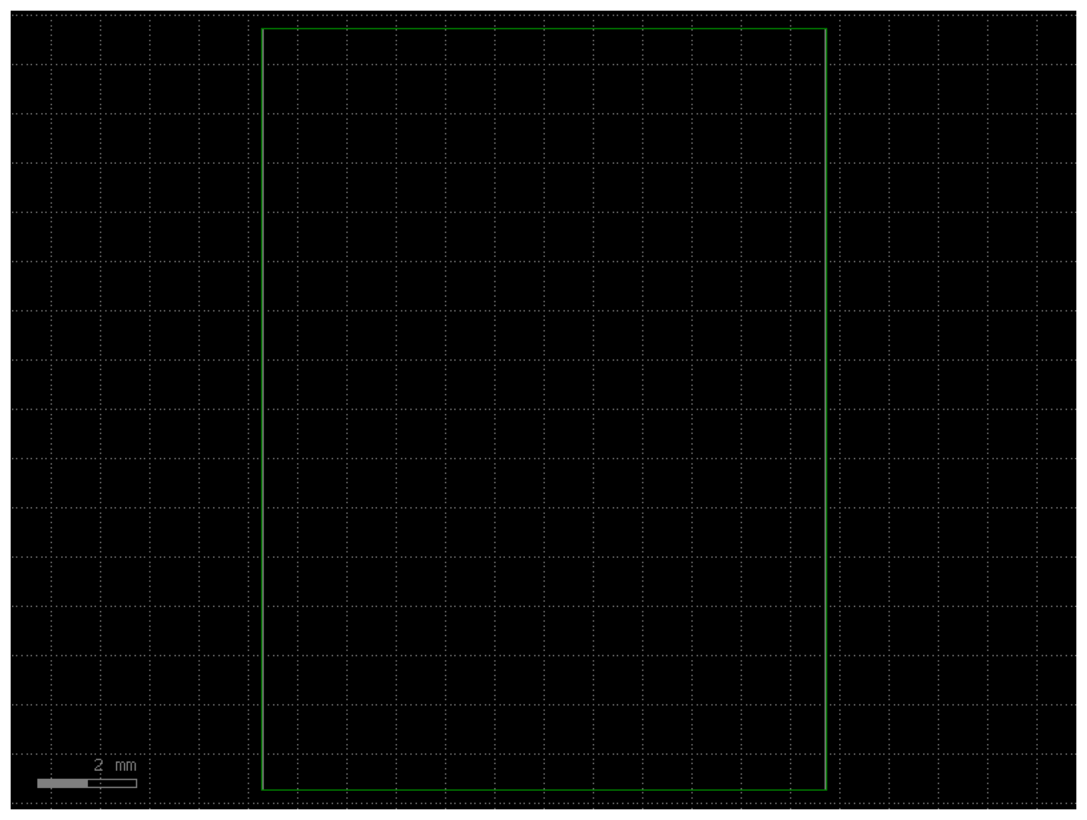
The Ge-on-Si user cell outline, centred on the origin.
Matches Cell0_Ge_on_Si_Institution_Name in the Cornerstone GDSII template and MPW-7 sec. 5.⅕.2: an 11.47 x 15.45 mm cell outline on layer 99 with 35 um bleed (dicing) strips on layer 98 inside the east and west edges. Edge-coupler waveguides must extend fully into the bleed strips.
Parameters:
| Name | Type | Description | Default |
|---|---|---|---|
size
|
tuple[float, float]
|
cell outline (width, height) in um. |
(11470.0, 15450.0)
|
bleed_width
|
float
|
width of the east/west bleed strips in um. |
35.0
|
:noindex:
from cspdk.ge_on_si import cells, PDK

PDK.activate()

c = cells.die(size=(11470, 15450), bleed_width=35)
c.draw_ports()
c.plot()
rectangle
A rectangle.
Parameters:
| Name | Type | Description | Default |
|---|---|---|---|
layer
|
LAYER.FLOORPLAN. |
FLOORPLAN
|
|
**kwargs
|
additional arguments. |
{}
|
:noindex:
from cspdk.ge_on_si import cells, PDK

PDK.activate()

c = cells.rectangle(layer='FLOORPLAN')
c.draw_ports()
c.plot()
straight
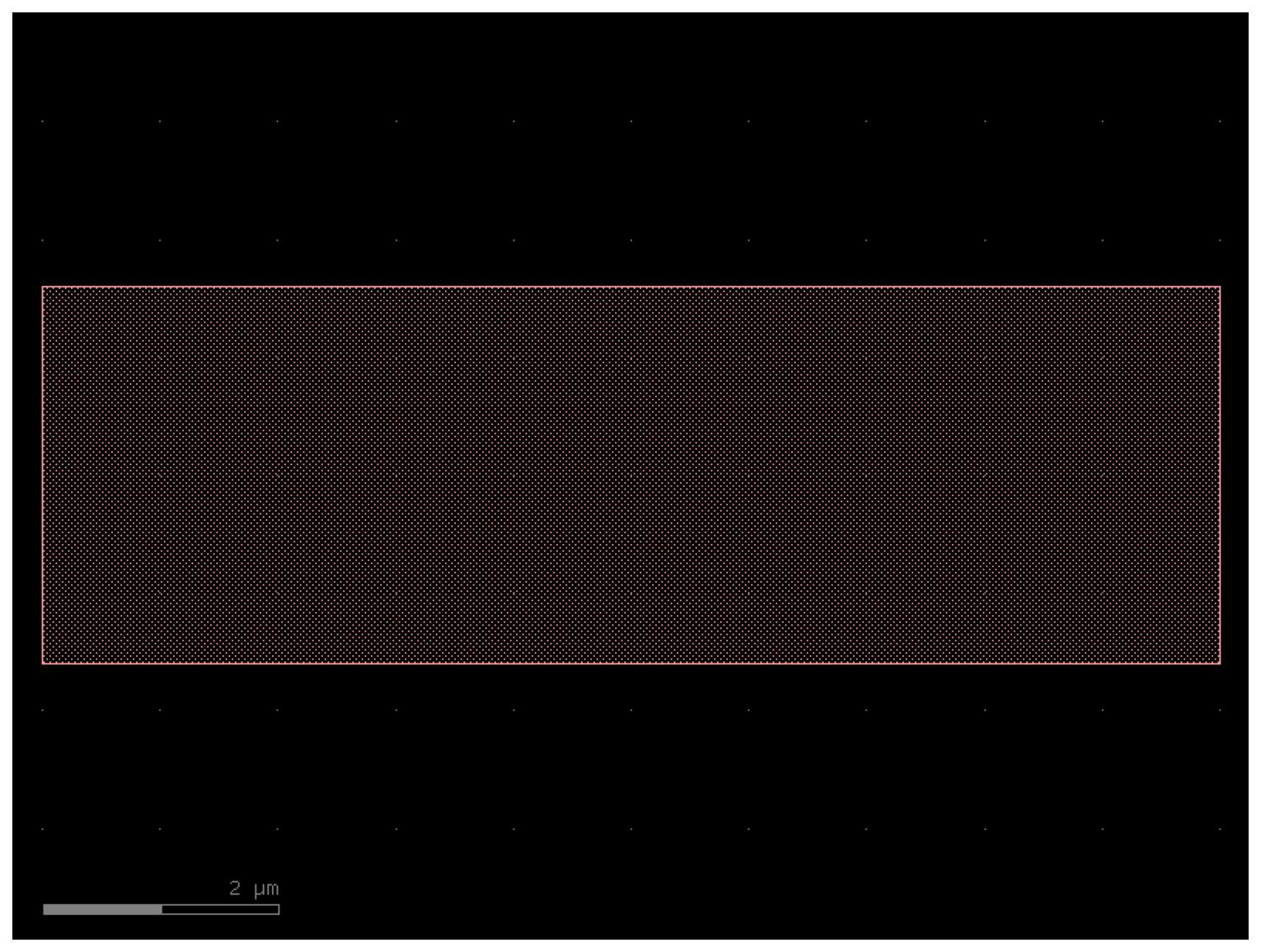
A straight waveguide.
Parameters:
| Name | Type | Description | Default |
|---|---|---|---|
length
|
float
|
the length of the waveguide. |
10.0
|
cross_section
|
CrossSectionSpec
|
a cross section or its name or a function generating a cross section. |
'xs_rib'
|
kwargs
|
additional arguments to pass to the straight function. |
{}
|
:noindex:
from cspdk.ge_on_si import cells, PDK

PDK.activate()

c = cells.straight(length=10, cross_section='xs_rib')
c.draw_ports()
c.plot()
taper
A taper.
Parameters:
| Name | Type | Description | Default |
|---|---|---|---|
length
|
float
|
the length of the taper. |
10.0
|
width1
|
float
|
the input width of the taper. |
width_rib
|
width2
|
float | None
|
the output width of the taper (if not given, use port). |
None
|
port
|
Port | None
|
the port (with certain width) to taper towards (if not given, use width2). |
None
|
cross_section
|
CrossSectionSpec
|
a cross section or its name or a function generating a cross section. |
'xs_rib'
|
:noindex: