Palace CPW Simulation — Wave Ports
Palace is an open-source 3D electromagnetic simulator supporting eigenmode, driven (S-parameter), and electrostatic simulations. This notebook demonstrates using the gsim.palace API to run a driven simulation on a CPW (coplanar waveguide) structure with wave ports.
Requirements:
- IHP PDK:
uv pip install ihp-gdsfactory - GDSFactory+ account for cloud simulation
Define GSG electrode
import gdsfactory as gf
from ihp import LAYER, PDK
PDK.activate()
@gf.cell
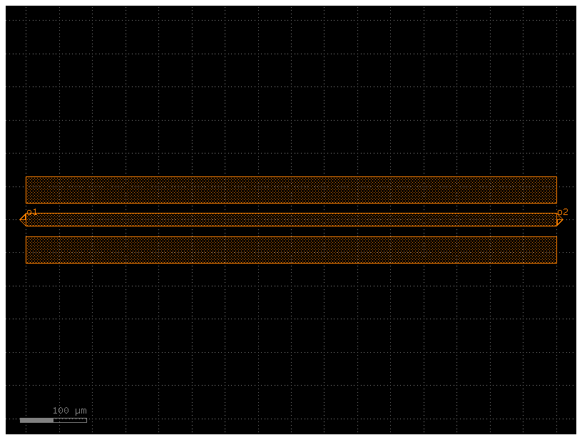
def gsg_electrode(
length: float = 800,
s_width: float = 20,
g_width: float = 40,
gap_width: float = 15,
layer=LAYER.TopMetal2drawing,
) -> gf.Component:
"""
Create a GSG (Ground-Signal-Ground) electrode.
Args:
length: horizontal length of the electrodes
s_width: width of the signal (center) electrode
g_width: width of the ground electrodes
gap_width: gap between signal and ground electrodes
layer: layer for the metal
"""
c = gf.Component()
r1 = c << gf.c.rectangle((length, g_width), centered=True, layer=layer)
r1.move((0, (g_width + s_width) / 2 + gap_width))
_r2 = c << gf.c.rectangle((length, s_width), centered=True, layer=layer)
r3 = c << gf.c.rectangle((length, g_width), centered=True, layer=layer)
r3.move((0, -(g_width + s_width) / 2 - gap_width))
c.add_port(
name="o1",
center=(-length / 2, 0),
width=s_width,
orientation=180,
port_type="electrical",
layer=layer,
)
c.add_port(
name="o2",
center=(length / 2, 0),
width=s_width,
orientation=0,
port_type="electrical",
layer=layer,
)
return c
c = gsg_electrode()
cc = c.copy()
cc.draw_ports()
cc
Configure simulation
from gsim.common.stack import get_stack
from gsim.palace import DrivenSim

sim = DrivenSim()
sim.set_output_dir("./palace-sim-cpw-waveport")
sim.set_geometry(c)

stack = get_stack()  # auto-detects active PDK
sim.set_stack(stack)
sim.set_airbox(margin_x=0.0, margin_y=50, z_above=100.0, z_below=100.0)

# Wave ports — max_size fills the full domain boundary
sim.add_wave_port("o1", layer="topmetal2", max_size=True, mode=1, excited=True)
sim.add_wave_port("o2", layer="topmetal2", max_size=True, mode=1, excited=False)

sim.set_driven(fmin=1e9, fmax=100e9, num_points=300)

print(sim.validate_config())
Validation: PASSED
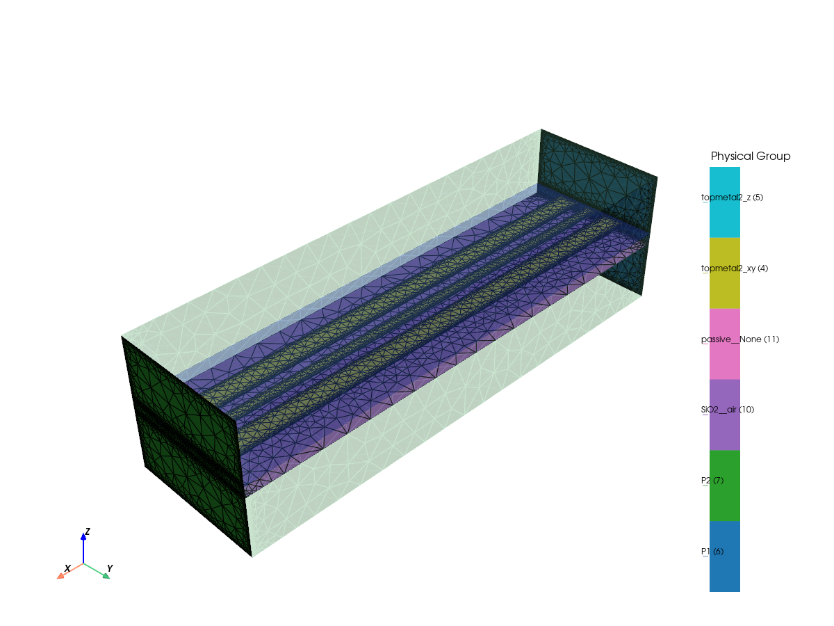
Generate mesh
Mesh Summary
========================================
Dimensions: 800.0 x 330.0 x 217.9 µm
Nodes:      43,804
Elements:   314,587
Tetrahedra: 231,039
Edge length: 1.08 - 79.63 µm
Quality:    0.634 (min: 0.000)
SICN:       0.685 (all valid)
----------------------------------------
Volumes (3):
  - si [1]
  - sin [2]
  - air [3]
Surfaces (9):
  - topmetal2_xy [4]
  - topmetal2_z [5]
  - P1 [6]
  - P2 [7]
  - si__None [8]
  - air__si [9]
  - si__sin [10]
  - air__sin [11]
  - air__None [12]
----------------------------------------
Mesh:   palace-sim-cpw-waveport/palace.msh
sim.plot_mesh(
    style="solid",
    transparent_groups=["air__None", "SiO2__None", "SiO2__passive", "air__passive"],
    interactive=True,
)
Run simulation
  palace-1ce34fb3  completed  9m 24s


Extracting results.tar.gz...
Downloaded 8 files to sim-data-palace-1ce34fb3
Plot S-parameters
Port mapping: Port 1: p1, Port 2: p2
Port mapping: Port 1: p1, Port 2: p2