Die and mask assembly
With gdsfactory you can easily go from a simple component, to a component with many components inside.
In the same way that you need to Layout for DRC (Design Rule Check) clean devices, you have to layout obeying the Design for Test (DFT) and Design for Packaging rules.
Design for Test
To measure your chips after fabrication you need to decide your test configurations. This includes Design For Testing Rules like:
Individual input and output fibersversusfiber array. You can useadd_fiber_arrayfor easier testing and higher throughput, oradd_fiber_singlefor the flexibility of single fibers.- Fiber array pitch (127um or 250um) if using a fiber array.
- Pad pitch for DC and RF high speed probes (100, 125, 150, 200um). Probe configuration (GSG, GS ...)
- Test layout for DC, RF and optical fibers.
from functools import partial

import gdsfactory as gf


gf.gpdk.PDK.activate()
# After you run gf.config.rich_output(), gdsfactory will automatically generate and display a plot of the component's geometry instead of the text.
gf.config.rich_output()
Pack
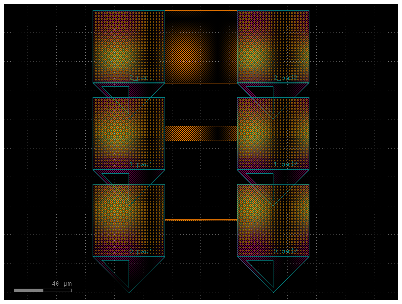
Let us start with a resistance sweep, where you change the resistance width to measure sheet resistance.
def add_resistance_sweep_info(c):
    # A helper function is defined to add specific metadata to a component's .info attribute.
    # This information, like "doe": "resistance_sweep" (Design of Experiments) and "measurement": "iv" (current-voltage),
    # is used by automated testing and data analysis tools.
    c.info["doe"] = "resistance_sweep"
    c.info["analysis"] = "[iv_resistance]"
    c.info["analysis_parameters"] = "[{}]"
    c.info["ports_electrical"] = 2
    c.info["ports_optical"] = 0
    c.info["measurement"] = "iv"
    c.info["measurement_parameters"] = "{}"
    return c

# A list of three resistance_sheet components is created, each with a different width (1, 10, and 50 µm).
sweep = [gf.components.resistance_sheet(width=width) for width in [1, 10, 50]]

# The add_resistance_sweep_info function is applied to each of the three resistor components, embedding the testing metadata into each one.
sweep_with_info = [add_resistance_sweep_info(c) for c in sweep]

# The gf.pack function takes the list of three components and automatically arranges them in a compact way,
# creating a single, larger component that contains them. m[0] retrieves this final packed component.
m = gf.pack(sweep_with_info)
c = m[0]
c.draw_ports()
c.pprint_ports()
c.plot()
┏━━━━━━━━┳━━━━━━━┳━━━━━━━━━━━━━┳━━━━━━━━━━━┳━━━━━━━━━━━━━━━━━━┳━━━━━━━━━━━━┓
┃ name   ┃ width ┃ orientation ┃ layer     ┃ center           ┃ port_type  ┃
┡━━━━━━━━╇━━━━━━━╇━━━━━━━━━━━━━╇━━━━━━━━━━━╇━━━━━━━━━━━━━━━━━━╇━━━━━━━━━━━━┩
│ 0_pad1 │ 50.0  │ 270.0       │ M3 (49/0) │ (30.05, 5.05)    │ electrical │
│ 0_pad2 │ 50.0  │ 270.0       │ M3 (49/0) │ (130.05, 5.05)   │ electrical │
│ 1_pad1 │ 50.0  │ 270.0       │ M3 (49/0) │ (30.05, 65.05)   │ electrical │
│ 1_pad2 │ 50.0  │ 270.0       │ M3 (49/0) │ (130.05, 65.05)  │ electrical │
│ 2_pad1 │ 50.0  │ 270.0       │ M3 (49/0) │ (30.05, 125.05)  │ electrical │
│ 2_pad2 │ 50.0  │ 270.0       │ M3 (49/0) │ (130.05, 125.05) │ electrical │
└────────┴───────┴─────────────┴───────────┴──────────────────┴────────────┘
sweep_with_info[0].info
[1;35mInfo[0m[1m([0m
[33mresistance[0m=[1;36m0[0m,
[33mlength[0m=[1;36m50[0m,
[33mwidth[0m=[1;36m1[0m,
[33mdoe[0m=[32m'resistance_sweep'[0m,
[33manalysis[0m=[32m'[0m[32m[[0m[32miv_resistance[0m[32m][0m[32m'[0m,
[33manalysis_parameters[0m=[32m'[0m[32m[[0m[32m{[0m[32m}[0m[32m][0m[32m'[0m,
[33mports_electrical[0m=[1;36m2[0m,
[33mports_optical[0m=[1;36m0[0m,
[33mmeasurement[0m=[32m'iv'[0m,
[33mmeasurement_parameters[0m=[32m'[0m[32m{[0m[32m}[0m[32m'[0m
[1m)[0m
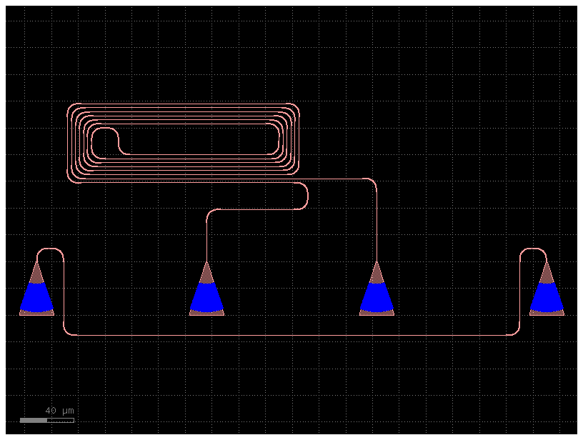
Then we add spirals with different lengths to measure the waveguide propagation loss. You can use both a fiber array or single fiber.
@gf.cell

# This line creates the basic spiral waveguide. The **kwargs allows you to pass any parameters (like length, width, etc.) to the underlying spiral component.
def spiral_gc(**kwargs):
    """Returns spiral with Grating Couplers."""
    c = gf.components.spiral(**kwargs)
    c = gf.routing.add_fiber_array(c)
    c.info["doe"] = "spirals_sc"  # Strip Cband spirals
    c.info["measurement"] = "optical_spectrum"
    c.info["measurement_parameters"] = "{}"
    c.info["analysis"] = "[power_envelope]"
    c.info["analysis_parameters"] = "[]"
    c.info["ports_optical"] = 4
    c.info["ports_electrical"] = 0
    c.info.update(kwargs)
    return c


c = spiral_gc(length=100)
c.plot()
c.info
[1;35mInfo[0m[1m([0m
[33mlength[0m=[1;36m100[0m,
[33mdoe[0m=[32m'spirals_sc'[0m,
[33mmeasurement[0m=[32m'optical_spectrum'[0m,
[33mmeasurement_parameters[0m=[32m'[0m[32m{[0m[32m}[0m[32m'[0m,
[33manalysis[0m=[32m'[0m[32m[[0m[32mpower_envelope[0m[32m][0m[32m'[0m,
[33manalysis_parameters[0m=[32m'[0m[32m[[0m[32m][0m[32m'[0m,
[33mports_optical[0m=[1;36m4[0m,
[33mports_electrical[0m=[1;36m0[0m
[1m)[0m
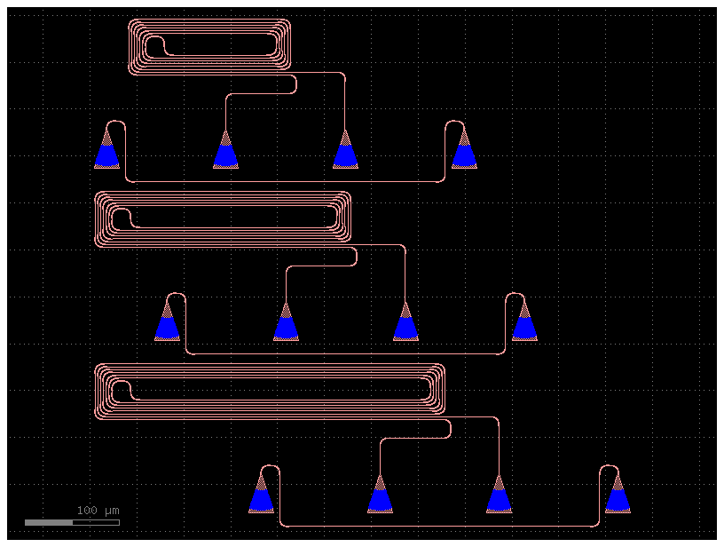
sweep = [spiral_gc(length=length) for length in [100, 200, 300]]
m = gf.pack(sweep)
c = m[0]
c.plot()
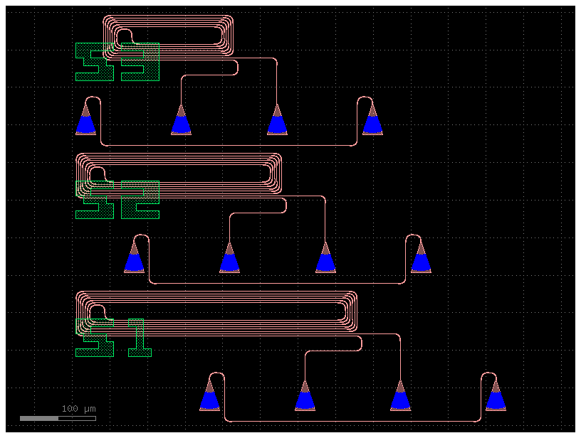
You can also add some physical labels that will be fabricated.
For example you can add prefix S at the north-center of each spiral using text_rectangular which is DRC clean and anchored on nc (north-center).
text_metal = partial(gf.components.text_rectangular_multi_layer, layers=("M1",))

m = gf.pack(sweep, text=text_metal, text_anchors=("cw",), text_prefix="s")
c = m[0]
c.show()
c.plot()
Grid
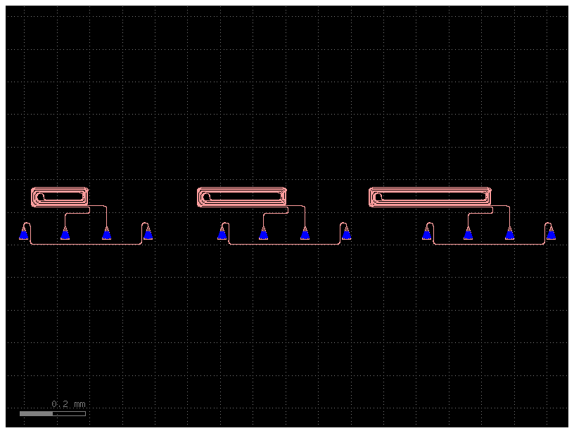
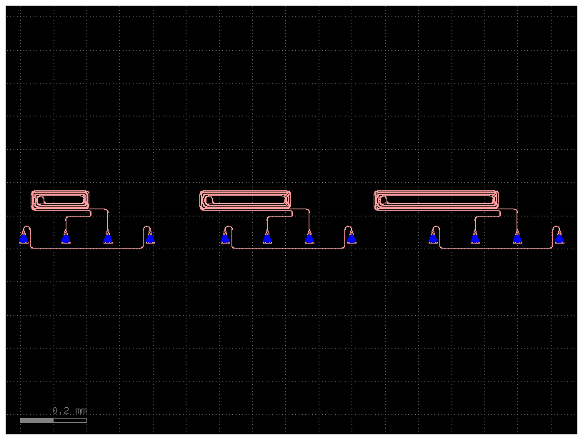
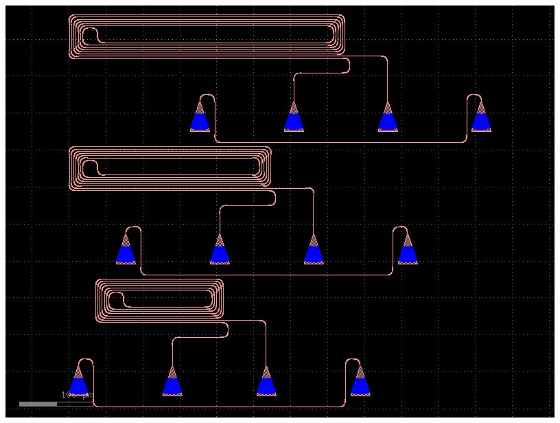
You can also pack components with a constant spacing.
g = gf.grid(sweep)
g.plot()
gh = gf.grid(sweep, shape=(1, len(sweep)))
gh.plot()
gh_ymin = gf.grid(sweep, shape=(len(sweep), 1), align_x="xmin")
gh_ymin.plot()
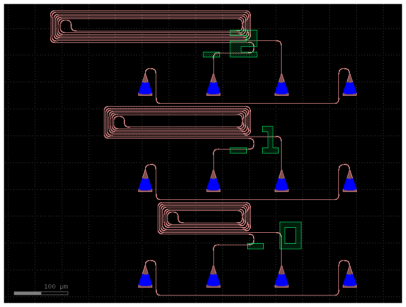
Additionally, it allows you to add text labels to each element of the sweep
gh_ymin = gf.grid_with_text(

    # shape=(len(sweep), 1): This defines the grid as having a single column and a number of rows equal to the number of components in the sweep list.
    # align_x="xmax": This aligns all the components in the column so that their right edges (xmax) are in a straight vertical line.
    # text=text_metal: This provides a list of text strings that will be placed as labels next to each corresponding component in the grid.
    sweep, shape=(len(sweep), 1), align_x="xmax", text=text_metal
)
gh_ymin.plot()
gh_ymin = gf.grid_with_text(
    sweep,
    shape=(len(sweep), 1),
    align_x="xmax",
    text=text_metal,
    labels=("S100", "S200", "S300"),
)
gh_ymin.plot()
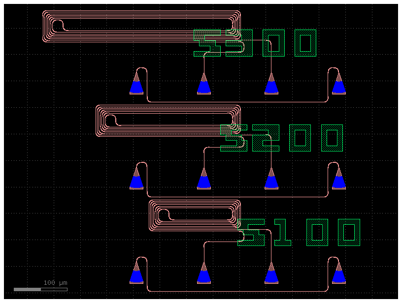
You have 2 ways of defining a mask:
- in YAML
- in Python
YAML Component
You can also define your Component in the YAML format thanks to gdsfactory.read.from_yaml
You need to define:
- Instances
- Placements
- Routes (optional)
And you can leverage:
pack_doepack_doe_grid
pack_doe places components as compact as possible.
pack_doe_grid places each component on a regular grid.
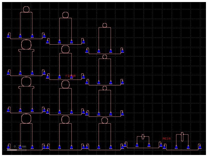
c = gf.read.from_yaml(
    """
name: mask_compact

instances:
  rings:

  #  This is a special function that creates a Design of Experiments array.
    component: pack_doe
    settings:

      # settings: radius: [30, 50, 20, 40], length_x: [1, 2, 3]: It will create ring resonators with these different radii and coupling lengths.
      doe: ring_single
      settings:
        radius: [30, 50, 20, 40]
        length_x: [1, 2, 3]

      # This tells the function to generate all possible combinations of the specified radius and length_x values.
      do_permutations: True
      function:

        # After each unique ring is created, the add_fiber_array function is applied to it, adding grating couplers for testing.
        function: add_fiber_array
        settings:
            fanout_length: 200


  mzis:
    component: pack_doe_grid
    settings:
      doe: mzi
      settings:
        delta_length: [10, 100]
      do_permutations: True
      spacing: [10, 10]
      function: add_fiber_array

placements:
  rings:
    xmin: 50

  mzis:
    xmin: rings,east
"""
)

c.show()
c.plot()
Automated testing and analysis
This is useful when you have a lot of components and you want to automate the testing process.
There are two main ways to define which components are testable:
- Include a
doe(Design of Experiments) field in the component.info dictionary, as well as all relevant test and analysis information. - Include a GDS label in all component test points. There are many ways to define test points, but the most common is to use a GDS label with the format
<elec/opt>-<number_of_ports>-<cell_name>. This way you can easily extract all test points from the GDS file.
import pandas as pd

import gdsfactory as gf


@gf.cell
def mzm_gc(length_x=10, **kwargs) -> gf.Component:
    """Returns a MZI with Grating Couplers.

    Args:
        length_x: length of the MZI.
        kwargs: additional settings.
    """
    c = gf.components.mzi2x2_2x2_phase_shifter(
        length_x=length_x, auto_rename_ports=False, **kwargs
    )
    c = gf.routing.add_pads_top(c, port_names=["top_l_e1", "top_r_e3"])
    c = gf.routing.add_fiber_array(c)
    c.info["doe"] = "mzm"
    c.info["measurement"] = "optical_spectrum"
    c.info["analysis"] = "[fsr]"
    c.info["analysis_parameters"] = "[]"
    c.info["ports_electrical"] = 2
    c.info["ports_optical"] = 6
    c.info["length_x"] = length_x
    c.info.update(kwargs)
    return c


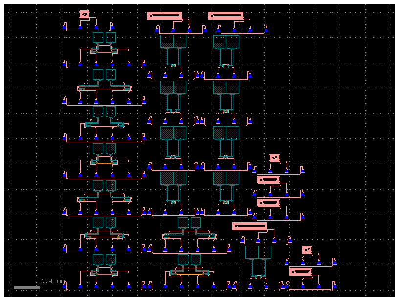
def sample_reticle(grid: bool = False) -> gf.Component:
    """Returns MZI with TE grating couplers."""

    mzis = [mzm_gc(length_x=lengths) for lengths in [100, 200, 300]]
    spirals = [spiral_gc(length=length) for length in [0, 100, 200]]
    rings = []
    for length_x in [10, 20, 30]:
        ring = gf.components.ring_single_heater(length_x=length_x)
        c = gf.components.add_fiber_array_optical_south_electrical_north(
            component=ring,
            electrical_port_names=["l_e2", "r_e2"],
            grating_coupler=gf.components.grating_coupler_te,
            pad=gf.components.pad,
            cross_section_metal='metal3'
        ).copy()
        c.name = f"ring_{length_x}"
        c.info["doe"] = "ring_length_x"
        c.info["measurement"] = "optical_spectrum"
        c.info["ports_electrical"] = 2
        c.info["ports_optical"] = 4
        c.info["analysis"] = "[fsr]"
        c.info["analysis_parameters"] = "[]"
        c.info["length_x"] = length_x
        rings.append(c)

    copies = 3  # Number of copies of each component.
    components = mzis * copies + rings * copies + spirals * copies
    if grid:
        return gf.grid(components)
    mask = gf.pack(components)
    if len(mask) > 1:
        mask = gf.pack(mask)
    return mask[0]


c = sample_reticle()
c.show()
c
gf.labels.write_test_manifest(c, csvpath="sample_reticle.csv")
df = pd.read_csv("sample_reticle.csv")
df
Warning: 'measurement_parameters' missing from 'mzm_gc_LX100'
Warning: 'measurement_parameters' missing from 'mzm_gc_LX200'
Warning: 'measurement_parameters' missing from 'mzm_gc_LX300'
Warning: 'measurement_parameters' missing from 'mzm_gc_LX100'
Warning: 'measurement_parameters' missing from 'mzm_gc_LX200'
Warning: 'measurement_parameters' missing from 'mzm_gc_LX300'
Warning: 'measurement_parameters' missing from 'mzm_gc_LX100'
Warning: 'measurement_parameters' missing from 'mzm_gc_LX200'
Warning: 'measurement_parameters' missing from 'mzm_gc_LX300'
Warning: 'measurement_parameters' missing from 'ring_10'
Warning: 'measurement_parameters' missing from 'ring_20'
Warning: 'measurement_parameters' missing from 'ring_30'
Warning: 'measurement_parameters' missing from 'ring_10'
Warning: 'measurement_parameters' missing from 'ring_20'
Warning: 'measurement_parameters' missing from 'ring_30'
Warning: 'measurement_parameters' missing from 'ring_10'
Warning: 'measurement_parameters' missing from 'ring_20'
Warning: 'measurement_parameters' missing from 'ring_30'
| cell | x | y | info | ports | settings | doe | analysis | analysis_parameters | measurement | measurement_parameters | ports_optical | ports_electrical | |
|---|---|---|---|---|---|---|---|---|---|---|---|---|---|
| 0 | mzm_gc_LX100 | 250.020 | 153.226 | {"length_x": 100} | {"in_o1": {"name": "in_o1", "center": [145020,... | {"length_x":100} | mzm | [fsr] | [] | optical_spectrum | NaN | 6 | 2 |
| 1 | mzm_gc_LX200 | 200.020 | 445.275 | {"length_x": 200} | {"in_o1": {"name": "in_o1", "center": [145020,... | {"length_x":200} | mzm | [fsr] | [] | optical_spectrum | NaN | 6 | 2 |
| 2 | mzm_gc_LX300 | 150.020 | 737.326 | {"length_x": 300} | {"in_o1": {"name": "in_o1", "center": [145020,... | {"length_x":300} | mzm | [fsr] | [] | optical_spectrum | NaN | 6 | 2 |
| 3 | mzm_gc_LX100 | 250.020 | 1029.376 | {"length_x": 100} | {"in_o1": {"name": "in_o1", "center": [145020,... | {"length_x":100} | mzm | [fsr] | [] | optical_spectrum | NaN | 6 | 2 |
| 4 | mzm_gc_LX200 | 200.020 | 1321.426 | {"length_x": 200} | {"in_o1": {"name": "in_o1", "center": [145020,... | {"length_x":200} | mzm | [fsr] | [] | optical_spectrum | NaN | 6 | 2 |
| 5 | mzm_gc_LX300 | 150.020 | 1613.476 | {"length_x": 300} | {"in_o1": {"name": "in_o1", "center": [145020,... | {"length_x":300} | mzm | [fsr] | [] | optical_spectrum | NaN | 6 | 2 |
| 6 | mzm_gc_LX100 | 250.020 | 1905.526 | {"length_x": 100} | {"in_o1": {"name": "in_o1", "center": [145020,... | {"length_x":100} | mzm | [fsr] | [] | optical_spectrum | NaN | 6 | 2 |
| 7 | mzm_gc_LX200 | 870.960 | 153.226 | {"length_x": 200} | {"in_o1": {"name": "in_o1", "center": [815960,... | {"length_x":200} | mzm | [fsr] | [] | optical_spectrum | NaN | 6 | 2 |
| 8 | mzm_gc_LX300 | 820.960 | 445.275 | {"length_x": 300} | {"in_o1": {"name": "in_o1", "center": [815960,... | {"length_x":300} | mzm | [fsr] | [] | optical_spectrum | NaN | 6 | 2 |
| 9 | ring_10 | 884.460 | 684.701 | {"length_x": 10} | {"o1": {"name": "o1", "center": [815960, 61821... | {"component":"ring_double_heater_gdsfactorypco... | ring_length_x | [fsr] | [] | optical_spectrum | NaN | 4 | 2 |
| 10 | ring_20 | 889.460 | 1044.701 | {"length_x": 20} | {"o1": {"name": "o1", "center": [815960, 97821... | {"component":"ring_double_heater_gdsfactorypco... | ring_length_x | [fsr] | [] | optical_spectrum | NaN | 4 | 2 |
| 11 | ring_30 | 894.460 | 1404.701 | {"length_x": 30} | {"o1": {"name": "o1", "center": [815960, 13382... | {"component":"ring_double_heater_gdsfactorypco... | ring_length_x | [fsr] | [] | optical_spectrum | NaN | 4 | 2 |
| 12 | ring_10 | 884.460 | 1764.701 | {"length_x": 10} | {"o1": {"name": "o1", "center": [815960, 16982... | {"component":"ring_double_heater_gdsfactorypco... | ring_length_x | [fsr] | [] | optical_spectrum | NaN | 4 | 2 |
| 13 | ring_20 | 1306.400 | 684.701 | {"length_x": 20} | {"o1": {"name": "o1", "center": [1232900, 6182... | {"component":"ring_double_heater_gdsfactorypco... | ring_length_x | [fsr] | [] | optical_spectrum | NaN | 4 | 2 |
| 14 | ring_30 | 1565.400 | 100.601 | {"length_x": 30} | {"o1": {"name": "o1", "center": [1486900, 3411... | {"component":"ring_double_heater_gdsfactorypco... | ring_length_x | [fsr] | [] | optical_spectrum | NaN | 4 | 2 |
| 15 | ring_10 | 1301.400 | 1044.701 | {"length_x": 10} | {"o1": {"name": "o1", "center": [1232900, 9782... | {"component":"ring_double_heater_gdsfactorypco... | ring_length_x | [fsr] | [] | optical_spectrum | NaN | 4 | 2 |
| 16 | ring_20 | 1306.400 | 1404.701 | {"length_x": 20} | {"o1": {"name": "o1", "center": [1232900, 1338... | {"component":"ring_double_heater_gdsfactorypco... | ring_length_x | [fsr] | [] | optical_spectrum | NaN | 4 | 2 |
| 17 | ring_30 | 1311.400 | 1764.701 | {"length_x": 30} | {"o1": {"name": "o1", "center": [1232900, 1698... | {"component":"ring_double_heater_gdsfactorypco... | ring_length_x | [fsr] | [] | optical_spectrum | NaN | 4 | 2 |
| 18 | spiral_gc_L200 | 1395.179 | 500.351 | {"length": 200, "text_label": "s2"} | {"o1": {"name": "o1", "center": [1551179, 3941... | {"length":200} | spirals_sc | [power_envelope] | [] | optical_spectrum | {} | 4 | 0 |
| 19 | spiral_gc_L200 | 724.239 | 2164.451 | {"length": 200, "text_label": "s2"} | {"o1": {"name": "o1", "center": [880239, 20582... | {"length":200} | spirals_sc | [power_envelope] | [] | optical_spectrum | {} | 4 | 0 |
| 20 | spiral_gc_L200 | 1205.459 | 2164.451 | {"length": 200, "text_label": "s2"} | {"o1": {"name": "o1", "center": [1361459, 2058... | {"length":200} | spirals_sc | [power_envelope] | [] | optical_spectrum | {} | 4 | 0 |
| 21 | spiral_gc_L100 | 1847.840 | 140.351 | {"length": 100, "text_label": "s3"} | {"o1": {"name": "o1", "center": [1903840, 3411... | {"length":100} | spirals_sc | [power_envelope] | [] | optical_spectrum | {} | 4 | 0 |
| 22 | spiral_gc_L100 | 1593.840 | 683.901 | {"length": 100, "text_label": "s3"} | {"o1": {"name": "o1", "center": [1649840, 5776... | {"length":100} | spirals_sc | [power_envelope] | [] | optical_spectrum | {} | 4 | 0 |
| 23 | spiral_gc_L100 | 1593.840 | 867.451 | {"length": 100, "text_label": "s3"} | {"o1": {"name": "o1", "center": [1649840, 7612... | {"length":100} | spirals_sc | [power_envelope] | [] | optical_spectrum | {} | 4 | 0 |
| 24 | spiral_gc_L0 | 1947.840 | 313.651 | {"length": 0} | {"o1": {"name": "o1", "center": [1903840, 2176... | {"length":0} | spirals_sc | [power_envelope] | [] | optical_spectrum | {} | 4 | 0 |
| 25 | spiral_gc_L0 | 189.020 | 2174.451 | {"length": 0} | {"o1": {"name": "o1", "center": [145020, 20784... | {"length":0} | spirals_sc | [power_envelope] | [] | optical_spectrum | {} | 4 | 0 |
| 26 | spiral_gc_L0 | 1693.840 | 1040.751 | {"length": 0} | {"o1": {"name": "o1", "center": [1649840, 9447... | {"length":0} | spirals_sc | [power_envelope] | [] | optical_spectrum | {} | 4 | 0 |
You can see a test manifest example here
Automated testing with labels
The GDS info is stored in the GDS file metadata and can be lost if the GDS file is modified with other tools that are not aware of the metadata. To avoid this, GDSFactory also supports a more traditional way of defining test points, using GDS labels.
For example, lets say you want to label the rightmost port of a component with a GDS label port_type-number_of_ports-cell_name. You can do this with the following code:
import gdsfactory as gf
from gdsfactory.typings import LayerSpec

layer_label = "TEXT"


def label_farthest_right_port(
    component: gf.Component, ports: gf.Port | list[gf.Port], layer: LayerSpec, text: str
) -> gf.Component:
    """Adds a label to the right of the farthest right port in a given component.

    Args:
        component: The component to which the label is added.
        ports: A list of ports to evaluate for positioning the label.
        layer: The layer on which the label will be added.
        text: The text to display in the label.
    """
    rightmost_port = max(ports, key=lambda port: port.x)

    component.add_label(
        text=text,
        position=rightmost_port.center,
        layer=layer,
    )
    return component


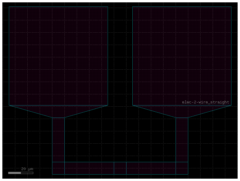
c = gf.Component()
ref = c << gf.routing.add_pads_top(gf.components.wire_straight())

# ref.ports: The function takes the list of all ports from the component reference ref.
# It then iterates through these ports to find the one with the largest x-coordinate (the one that is farthest to the right).
# c.add_label(...): Once the rightmost port is identified, the function adds a text label to the main component c at that port's position.
label_farthest_right_port(c, ref.ports, layer=layer_label, text="elec-2-wire_straight")
c
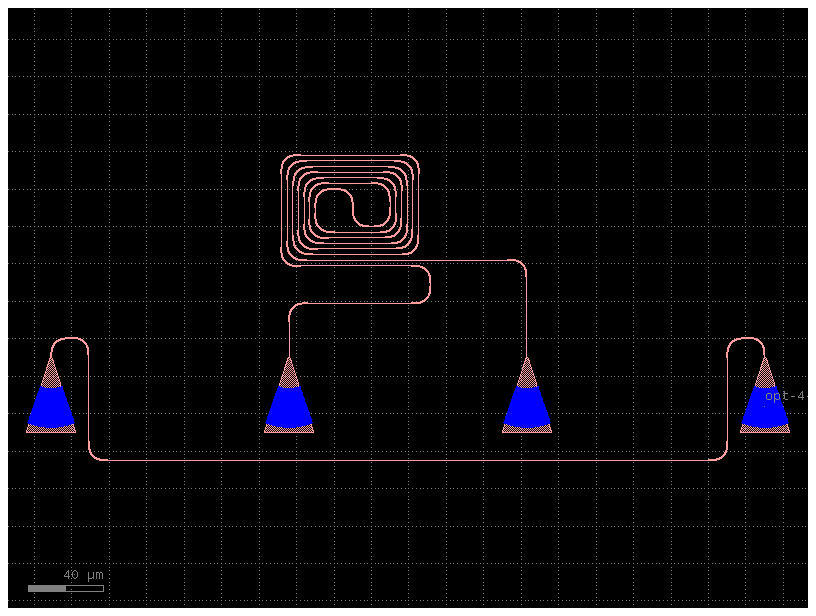
def spiral_gc(length: float = 0, **kwargs) -> gf.Component:
    """Returns a spiral double with Grating Couplers.

    Args:
        length: length of the spiral straight section.
        kwargs: additional settings.

    Keyword Args:
        bend: bend component.
        straight: straight component.
        cross_section: cross_section component.
        spacing: spacing between the spiral loops.
        n_loops: number of loops.
    """
    c0 = gf.c.spiral(length=length, **kwargs)
    c = gf.routing.add_fiber_array(c0)
    c.info["doe"] = "spirals_sc"
    c.info["measurement"] = "optical_spectrum"
    c.info["analysis"] = "[power_envelope]"
    c.info["analysis_parameters"] = "[]"
    c.info["ports_optical"] = 4
    c.info["ports_electrical"] = 0
    c.info.update(kwargs)

    c.name = f"spiral_gc_{length}"
    label_farthest_right_port(c, c.ports, layer=layer_label, text=f"opt-4-{c.name}")
    return c


c = spiral_gc(length=0)
c
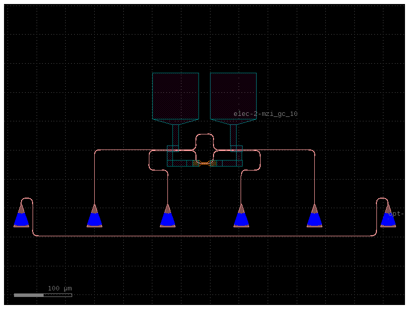
def mzi_gc(length_x=10, **kwargs) -> gf.Component:
    """Returns a MZI with Grating Couplers.

    Args:
        length_x: length of the MZI.
        kwargs: additional settings.
    """
    c = gf.components.mzi2x2_2x2_phase_shifter(
        length_x=length_x, auto_rename_ports=False, **kwargs
    )
    c = gf.routing.add_pads_top(c, port_names=("top_l_e1", "top_r_e3"))
    c.name = f"mzi_{length_x}"
    c = gf.routing.add_fiber_array(c)

    c.info["doe"] = "mzi"
    c.info["measurement"] = "optical_spectrum"
    c.info["analysis"] = "[fsr]"
    c.info["analysis_parameters"] = "[]"
    c.info["ports_electrical"] = 2
    c.info["ports_optical"] = 6
    c.info["length_x"] = length_x
    c.info.update(kwargs)

    c.name = f"mzi_gc_{length_x}"
    label_farthest_right_port(
        c,
        c.ports.filter(port_type="vertical_te"),
        layer=layer_label,
        text=f"opt-{c.info['ports_optical']}-{c.name}",
    )
    label_farthest_right_port(
        c,
        c.ports.filter(port_type="electrical"),
        layer=layer_label,
        text=f"elec-{c.info['ports_electrical']}-{c.name}",
    )
    return c


c = mzi_gc(length_x=10)
c
def sample_reticle_with_labels(grid: bool = False) -> gf.Component:
    """Returns MZI with TE grating couplers."""

    mzis = [mzi_gc(length_x=lengths) for lengths in [100, 200, 300]]
    spirals = [spiral_gc(length=length) for length in [0, 100, 200]]
    rings = []
    for length_x in [10, 20, 30]:
        ring = gf.components.ring_single_heater(length_x=length_x)
        c = gf.components.add_fiber_array_optical_south_electrical_north(
            component=ring,
            electrical_port_names=["l_e2", "r_e2"],
            grating_coupler=gf.components.grating_coupler_te,
            pad=gf.components.pad,
            cross_section_metal='metal3'
        ).copy()
        c.name = f"ring_{length_x}"
        c.info["doe"] = "ring_length_x"
        c.info["measurement"] = "optical_spectrum"
        c.info["ports_electrical"] = 2
        c.info["ports_optical"] = 4
        c.info["analysis"] = "[fsr]"
        c.info["analysis_parameters"] = "[]"
        label_farthest_right_port(
            c,
            c.ports.filter(port_type="vertical_te"),
            layer=layer_label,
            text=f"opt-{c.info['ports_optical']}-{c.name}",
        )
        label_farthest_right_port(
            c,
            c.ports.filter(port_type="electrical"),
            layer=layer_label,
            text=f"elec-{c.info['ports_electrical']}-{c.name}",
        )
        rings.append(c)

    copies = 3  # Number of copies of each component.
    components = mzis * copies + rings * copies + spirals * copies

    # gf.grid(components): This function is called to arrange the components in a simple, evenly spaced grid.
    if grid:
        return gf.grid(components)

    # gf.pack(components): This is the default path. The pack function uses a more advanced algorithm to arrange the components in a space-efficient way,
    # which is important for minimizing the cost of fabrication. This may result in a list of one or more packed groups.
    c = gf.pack(components)

    # The pack function can sometimes return multiple packed groups. This code checks if that is the case (len(c) > 1) and, if so,
    # runs pack again on those groups to combine them into one final, single component. The [0] then selects that final component.
    if len(c) > 1:
        c = gf.pack(c)[0]
    return c[0]


c = sample_reticle_with_labels()
c
[32m2026-10-11 13:27:29.801[0m | [31m[1mERROR [0m | [36mkfactory.kcell[0m:[36mname[0m:[36m824[0m - [31m[1mName conflict in kfactory.kcell::name at line 824
Renaming Unnamed_328 (cell_index=328) to spiral_gc_0 would cause it to be named the same as:
- spiral_gc_0 (cell_index=308), function_name=None, basename=None[0m
[32m2026-10-11 13:27:29.858[0m | [31m[1mERROR [0m | [36mkfactory.kcell[0m:[36mname[0m:[36m824[0m - [31m[1mName conflict in kfactory.kcell::name at line 824
Renaming add_fiber_array_optical_south_electrical_north_gdsfacto_5612d773$1 (cell_index=331) to ring_10 would cause it to be named the same as:
- ring_10 (cell_index=280), function_name=None, basename=None[0m
[32m2026-10-11 13:27:29.879[0m | [31m[1mERROR [0m | [36mkfactory.kcell[0m:[36mname[0m:[36m824[0m - [31m[1mName conflict in kfactory.kcell::name at line 824
Renaming add_fiber_array_optical_south_electrical_north_gdsfacto_d7ce6005$1 (cell_index=332) to ring_20 would cause it to be named the same as:
- ring_20 (cell_index=290), function_name=None, basename=None[0m
[32m2026-10-11 13:27:29.900[0m | [31m[1mERROR [0m | [36mkfactory.kcell[0m:[36mname[0m:[36m824[0m - [31m[1mName conflict in kfactory.kcell::name at line 824
Renaming add_fiber_array_optical_south_electrical_north_gdsfacto_c4c9a30b$1 (cell_index=333) to ring_30 would cause it to be named the same as:
- ring_30 (cell_index=300), function_name=None, basename=None[0m
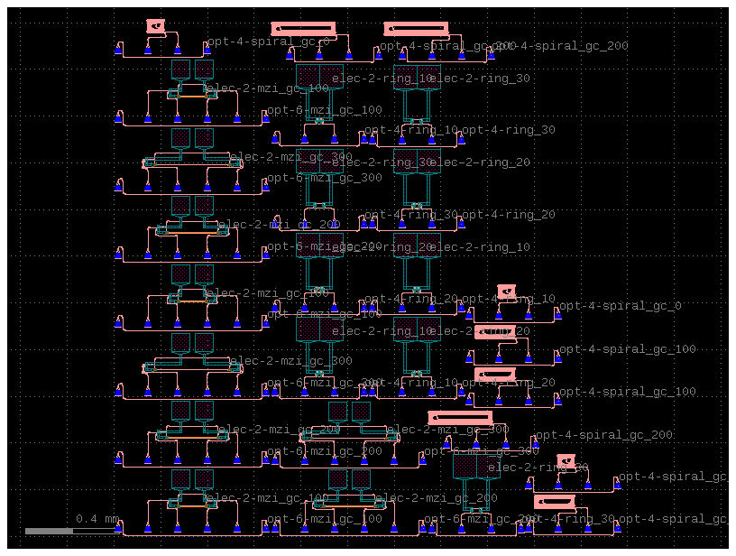
You can also extract all test points from a GDS file using gf.labels.write_labels
import pandas as pd

gdspath = c.write_gds()
csvpath = gf.labels.write_labels(gdspath, layer_label=layer_label)
df = pd.read_csv(csvpath)
df = df.sort_values(by=["text"])
df
| text | x | y | angle | |
|---|---|---|---|---|
| 13 | elec-2-mzi_gc_100 | 395.920 | 1877.401 | 0.0 |
| 1 | elec-2-mzi_gc_100 | 395.920 | 125.101 | 0.0 |
| 7 | elec-2-mzi_gc_100 | 395.920 | 1001.251 | 0.0 |
| 3 | elec-2-mzi_gc_200 | 445.920 | 417.150 | 0.0 |
| 9 | elec-2-mzi_gc_200 | 445.920 | 1293.301 | 0.0 |
| 15 | elec-2-mzi_gc_200 | 1116.860 | 125.101 | 0.0 |
| 5 | elec-2-mzi_gc_300 | 495.920 | 709.201 | 0.0 |
| 17 | elec-2-mzi_gc_300 | 1166.860 | 417.150 | 0.0 |
| 11 | elec-2-mzi_gc_300 | 495.920 | 1585.351 | 0.0 |
| 25 | elec-2-ring_10 | 929.460 | 1919.150 | 0.0 |
| 19 | elec-2-ring_10 | 929.460 | 839.150 | 0.0 |
| 31 | elec-2-ring_10 | 1346.400 | 1199.150 | 0.0 |
| 21 | elec-2-ring_20 | 929.460 | 1199.150 | 0.0 |
| 27 | elec-2-ring_20 | 1346.400 | 839.150 | 0.0 |
| 33 | elec-2-ring_20 | 1346.400 | 1559.150 | 0.0 |
| 29 | elec-2-ring_30 | 1600.400 | 255.050 | 0.0 |
| 35 | elec-2-ring_30 | 1346.400 | 1919.150 | 0.0 |
| 23 | elec-2-ring_30 | 929.460 | 1559.150 | 0.0 |
| 30 | opt-4-ring_10 | 1486.900 | 978.211 | 0.0 |
| 18 | opt-4-ring_10 | 1069.960 | 618.211 | 0.0 |
| 24 | opt-4-ring_10 | 1069.960 | 1698.211 | 0.0 |
| 32 | opt-4-ring_20 | 1486.900 | 1338.211 | 0.0 |
| 20 | opt-4-ring_20 | 1069.960 | 978.211 | 0.0 |
| 26 | opt-4-ring_20 | 1486.900 | 618.211 | 0.0 |
| 34 | opt-4-ring_30 | 1486.900 | 1698.211 | 0.0 |
| 28 | opt-4-ring_30 | 1740.900 | 34.111 | 0.0 |
| 22 | opt-4-ring_30 | 1069.960 | 1338.211 | 0.0 |
| 42 | opt-4-spiral_gc_0 | 2157.840 | 217.661 | 0.0 |
| 44 | opt-4-spiral_gc_0 | 1903.840 | 944.761 | 0.0 |
| 43 | opt-4-spiral_gc_0 | 399.020 | 2078.461 | 0.0 |
| 39 | opt-4-spiral_gc_100 | 2157.840 | 34.111 | 0.0 |
| 40 | opt-4-spiral_gc_100 | 1903.840 | 577.661 | 0.0 |
| 41 | opt-4-spiral_gc_100 | 1903.840 | 761.211 | 0.0 |
| 36 | opt-4-spiral_gc_200 | 1805.179 | 394.111 | 0.0 |
| 37 | opt-4-spiral_gc_200 | 1134.239 | 2058.211 | 0.0 |
| 38 | opt-4-spiral_gc_200 | 1615.459 | 2058.211 | 0.0 |
| 12 | opt-6-mzi_gc_100 | 653.020 | 1786.411 | 0.0 |
| 6 | opt-6-mzi_gc_100 | 653.020 | 910.261 | 0.0 |
| 0 | opt-6-mzi_gc_100 | 653.020 | 34.111 | 0.0 |
| 14 | opt-6-mzi_gc_200 | 1323.960 | 34.111 | 0.0 |
| 8 | opt-6-mzi_gc_200 | 653.020 | 1202.311 | 0.0 |
| 2 | opt-6-mzi_gc_200 | 653.020 | 326.160 | 0.0 |
| 16 | opt-6-mzi_gc_300 | 1323.960 | 326.160 | 0.0 |
| 10 | opt-6-mzi_gc_300 | 653.020 | 1494.361 | 0.0 |
| 4 | opt-6-mzi_gc_300 | 653.020 | 618.211 | 0.0 |