PDK#
gdsfactory includes a generic Process Design Kit (PDK), that you can use as an inspiration to create your own.
A process design kit (PDK) includes:
LayerStack: different layers with different thickness, z-position, materials and colors.
Design rule checking deck DRC: Manufacturing rules capturing min feature size, min spacing … for the process.
A library of Fixed or Parametric cells.
The PDK allows you to register:
cellparametric cells that return Components from a ComponentSpec (string, Component, ComponentFactory or dict). Also known as parametric cell functions.cross_sectionfunctions that return CrossSection from a CrossSection Spec (string, CrossSection, CrossSectionFactory or dict).layersthat return a GDS Layer (gdslayer, gdspurpose) from a string, an int or a Tuple[int, int].
Thanks to activating a PDK you can access components, cross_sections or layers using a string, a function or a dict.
Depending on the active pdk:
get_layerreturns a Layer from the registered layers.get_componentreturns a Component from the registered cells.get_cross_sectionreturns a CrossSection from the registered cross_sections.
layers#
GDS layers are a tuple of two integer number gdslayer/gdspurpose
You can define all the layers from your PDK:
From a Klayout
lyp(layer properties file).From scratch, adding all your layers into a class.
Lets generate the layers definition code from a KLayout lyp file.
import pathlib
from functools import partial

import pytest
from pytest_regressions.data_regression import DataRegressionFixture

import gdsfactory as gf
from gdsfactory.component import Component
from gdsfactory.config import PATH
from gdsfactory.decorators import has_valid_transformations
from gdsfactory.difftest import difftest
from gdsfactory.generic_tech import get_generic_pdk
from gdsfactory.technology import (
    LayerViews,
    lyp_to_dataclass,
    LayerMap,
)
from gdsfactory.typings import Layer, LayerSpec

gf.config.rich_output()
nm = 1e-3
class LayerMapDemo(LayerMap):
    WG: Layer = (1, 0)
    DEVREC: Layer = (68, 0)
    PORT: Layer = (1, 10)
    PORTE: Layer = (1, 11)
    LABEL_INSTANCES: Layer = (206, 0)
    LABEL_SETTINGS: Layer = (202, 0)
    LUMERICAL: Layer = (733, 0)
    M1: Layer = (41, 0)
    M2: Layer = (45, 0)
    M3: Layer = (49, 0)
    N: Layer = (20, 0)
    NP: Layer = (22, 0)
    NPP: Layer = (24, 0)
    OXIDE_ETCH: Layer = (6, 0)
    P: Layer = (21, 0)
    PDPP: Layer = (27, 0)
    PP: Layer = (23, 0)
    PPP: Layer = (25, 0)
    PinRec: Layer = (1, 10)
    PinRecM: Layer = (1, 11)
    SHALLOWETCH: Layer = (2, 6)
    SILICIDE: Layer = (39, 0)
    SIM_REGION: Layer = (100, 0)
    SITILES: Layer = (190, 0)
    SLAB150: Layer = (2, 0)
    SLAB150CLAD: Layer = (2, 9)
    SLAB90: Layer = (3, 0)
    SLAB90CLAD: Layer = (3, 1)
    SOURCE: Layer = (110, 0)
    TE: Layer = (203, 0)
    TEXT: Layer = (66, 0)
    TM: Layer = (204, 0)
    Text: Layer = (66, 0)
    VIA1: Layer = (44, 0)
    VIA2: Layer = (43, 0)
    VIAC: Layer = (40, 0)
    WGCLAD: Layer = (111, 0)
    WGN: Layer = (34, 0)
    WGclad_material: Layer = (36, 0)


LAYER = LayerMapDemo()
some generic components use some
Layer |
Purpose |
|---|---|
DEVREC |
device recognition layer. For connectivity checks. |
PORT |
optical port pins. For connectivity checks. |
PORTE |
electrical port pins. For connectivity checks. |
SHOW_PORTS |
add port pin markers when |
LABEL_INSTANCE |
for adding instance labels on |
MTOP |
for top metal routing |
class LayersConvenient(LayerMap):
    DEVREC: Layer = (68, 0)
    PORT: Layer = (1, 10)  # PinRec optical
    PORTE: Layer = (1, 11)  # PinRec electrical
    SHOW_PORTS: Layer = (1, 12)

    LABEL_INSTANCE: Layer = (66, 0)
    TE: Layer = (203, 0)
    TM: Layer = (204, 0)
cross_sections#
You can create a CrossSection from scratch or you can customize the cross_section functions in gf.cross_section
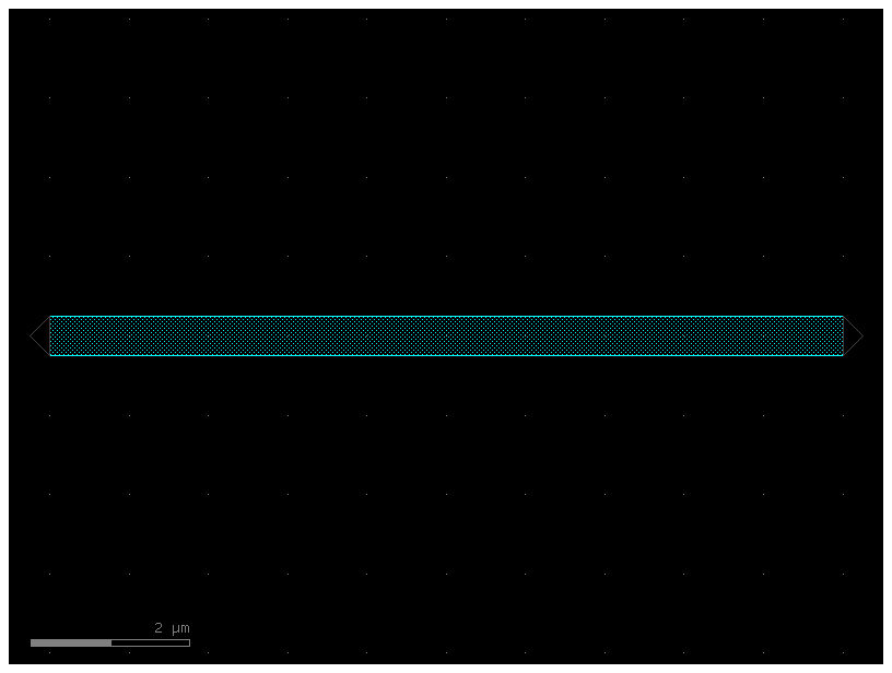
strip2 = partial(gf.cross_section.strip, layer=(2, 0))
c = gf.components.straight(cross_section=strip2)
c.plot()
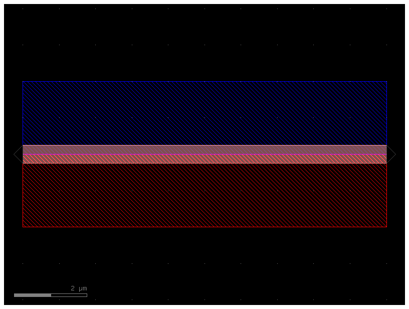
pin = partial(
    gf.cross_section.strip,
    sections=(
        gf.Section(width=2, layer=(20, 0), offset=+1),
        gf.Section(width=2, layer=(21, 0), offset=-1),
    ),
)
c = gf.components.straight(cross_section=pin)
c.plot()
strip_wide = partial(gf.cross_section.strip, width=3)
# auto_widen tapers to wider waveguides for lower loss in long straight sections.
strip = partial(gf.cross_section.strip, auto_widen=True)
xs_sc = strip()
xs_sc_wide = strip_wide()
xs_pin = pin()

cross_sections = dict(xs_sc_wide=xs_sc_wide, xs_pin=xs_pin, xs_sc=xs_sc)
2025-01-19 23:49:53.327 | WARNING | __main__:<module>:1 - UserWarning: auto_widen is deprecated. Pass this parameter to the routing function instead.
2025-01-19 23:49:53.329 | WARNING | __main__:<module>:1 - UserWarning: auto_widen is deprecated.
cells#
Cells are functions that return Components. They are parametrized and accept also cells as parameters, so you can build many levels of complexity. Cells are also known as PCells or parametric cells.
You can customize the function default arguments easily thanks to functools.partial
Lets customize the default arguments of a library of cells.
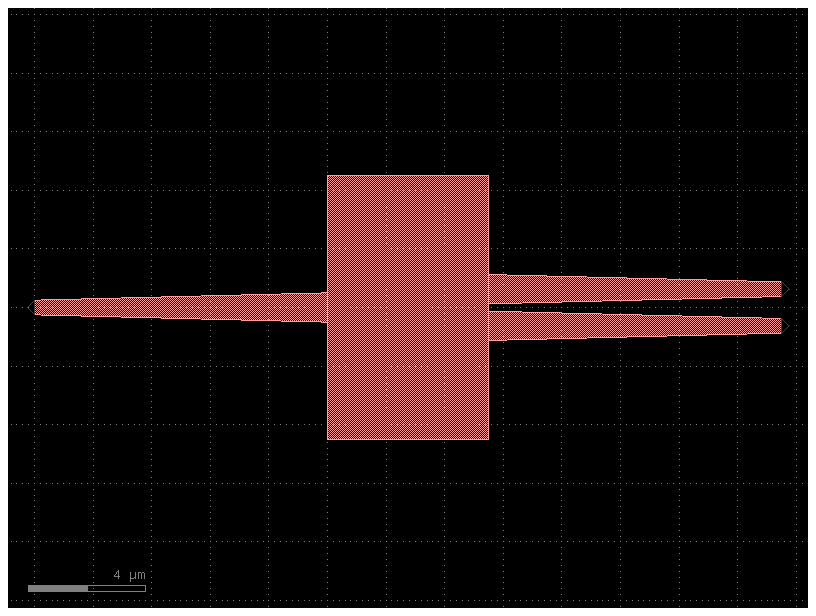
For example, you can make some wide MMIs for a particular technology. Lets say the best MMI width you found it to be 9um.
mmi1x2 = partial(gf.components.mmi1x2, width_mmi=9)
mmi2x2 = partial(gf.components.mmi2x2, width_mmi=9)

cells = dict(mmi1x2=mmi1x2, mmi2x2=mmi2x2)
You can define a new PDK by creating function that customize partial parameters of the generic functions.
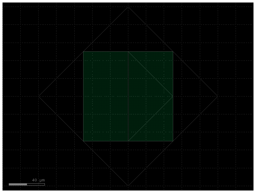
Lets say that this PDK uses layer (41, 0) for the pads (instead of the layer used in the generic pad function).
pad_custom_layer = partial(gf.components.pad, layer=(41, 0))
c = pad_custom_layer()
c.plot()
PDK#
You can register Layers, ComponentFactories (Parametric cells) and CrossSectionFactories (cross_sections) into a PDK.
Then you can access them by a string after you activate the pdk PDK.activate().
LayerSpec#
You can access layers from the active Pdk using the layer name or a tuple/list of two numbers.
from gdsfactory.generic_tech import get_generic_pdk

generic_pdk = get_generic_pdk()

pdk1 = gf.Pdk(
    name="fab1",
    layers=dict(LAYER),
    cross_sections=cross_sections,
    cells=cells,
    base_pdk=generic_pdk,
    layer_views=generic_pdk.layer_views,
)
pdk1.activate()
2025-01-19 23:49:53.495 | WARNING | gdsfactory.pdk:activate:289 - UserWarning: base_pdk is deprecated. Use base_pdks instead
pdk1.get_layer("WG")
(1, 0)
pdk1.get_layer([1, 0])
[1, 0]
CrossSectionSpec#
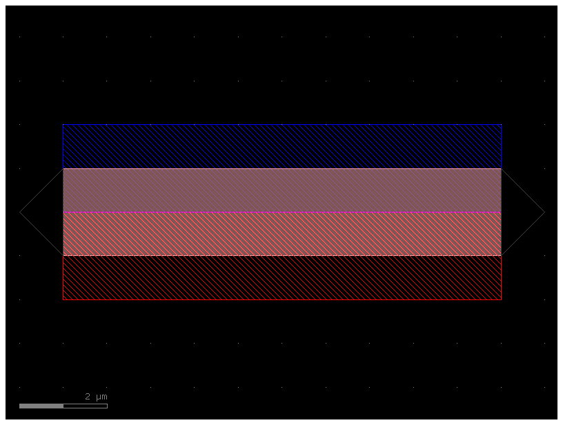
You can access cross_sections from the pdk from the cross_section name, or using a dict to customize the CrossSection
pdk1.get_cross_section("xs_pin")
CrossSection(
    sections=(
        Section(
            width=0.5,
            offset=0.0,
            insets=None,
            layer='WG',
            port_names=('o1', 'o2'),
            port_types=('optical', 'optical'),
            name='_default',
            hidden=False,
            simplify=None,
            width_function=None,
            offset_function=None
        ),
        Section(
            width=2.0,
            offset=1.0,
            insets=None,
            layer=(20, 0),
            port_names=(None, None),
            port_types=('optical', 'optical'),
            name=None,
            hidden=False,
            simplify=None,
            width_function=None,
            offset_function=None
        ),
        Section(
            width=2.0,
            offset=-1.0,
            insets=None,
            layer=(21, 0),
            port_names=(None, None),
            port_types=('optical', 'optical'),
            name=None,
            hidden=False,
            simplify=None,
            width_function=None,
            offset_function=None
        )
    ),
    components_along_path=(),
    radius=10.0,
    radius_min=5.0,
    bbox_layers=None,
    bbox_offsets=None
)
cross_section_spec_string = "xs_pin"
c = gf.components.straight(cross_section=cross_section_spec_string)
c.plot()

cross_section_spec_dict = dict(cross_section="xs_pin", settings=dict(width=2))
print(pdk1.get_cross_section(cross_section_spec_dict))
wg_pin = gf.components.straight(cross_section=cross_section_spec_dict)
wg_pin.plot()
2025-01-19 23:49:53.642 | WARNING | gdsfactory.pdk:get_cross_section:519 - UserWarning: CrossSection.copy() only modifies the attributes of the first section.
sections=(Section(width=2, offset=0.0, insets=None, layer='WG', port_names=('o1', 'o2'), port_types=('optical', 'optical'), name='_default', hidden=False, simplify=None, width_function=None, offset_function=None), Section(width=2.0, offset=1.0, insets=None, layer=(20, 0), port_names=(None, None), port_types=('optical', 'optical'), name=None, hidden=False, simplify=None, width_function=None, offset_function=None), Section(width=2.0, offset=-1.0, insets=None, layer=(21, 0), port_names=(None, None), port_types=('optical', 'optical'), name=None, hidden=False, simplify=None, width_function=None, offset_function=None)) components_along_path=() radius=10.0 radius_min=5.0 bbox_layers=None bbox_offsets=None
ComponentSpec#
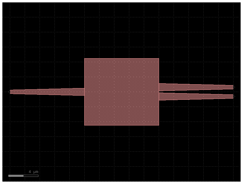
You can get Component from the active pdk using the cell name (string) or a dict.
c = pdk1.get_component("mmi1x2")
c.plot()
c = pdk1.get_component(dict(component="mmi1x2", settings=dict(length_mmi=10)))
c.plot()
Testing PDK cells#
To make sure all your PDK PCells produce the components that you want, it’s important to test your PDK cells.
As you write your own cell functions you want to make sure you do not break or produced unwanted regressions later on. You should write tests for this.
Make sure you create a test_components.py file for pytest to test your PDK. See for example the tests in the ubc PDK
Pytest-regressions automatically creates the CSV and YAML files for you, as well gdsfactory.gdsdiff will store the reference GDS in ref_layouts and check for geometry differences using XOR.
gdsfactory is not backwards compatible, which means that the package will keep improving and evolving.
To make your work stable you should install a specific version and pin the version in your
requirements.txtorpyproject.tomlasgdsfactory==7.27.2replacing7.27.2by whatever version you end up using.Before you upgrade gdsfactory to a newer version make sure your tests pass to make sure that things behave as expected
"""This code tests all your cells in the PDK

it will test 3 things:

1. difftest: will test the GDS geometry of a new GDS compared to a reference. Thanks to Klayout fast booleans.add()
2. settings test: will compare the settings in YAML with a reference YAML file.add()
3. ensure ports are on grid, to avoid port snapping errors that can create 1nm gaps later on when you build circuits.

"""

try:
    dirpath = pathlib.Path(__file__).absolute().with_suffix(".gds")
except Exception:
    dirpath = pathlib.Path.cwd()


component_names = list(pdk1.cells.keys())
factory = pdk1.cells


@pytest.fixture(params=component_names, scope="function")
def component_name(request) -> str:
    return request.param


def test_gds(component_name: str) -> None:
    """Avoid regressions in GDS names, shapes and layers.
    Runs XOR and computes the area."""
    component = factory[component_name]()
    test_name = f"fabc_{component_name}"
    difftest(component, test_name=test_name, dirpath=dirpath)


def test_settings(component_name: str, data_regression: DataRegressionFixture) -> None:
    """Avoid regressions in component settings and ports."""
    component = factory[component_name]()
    data_regression.check(component.to_dict())


def test_assert_ports_on_grid(component_name: str):
    """Ensures all ports are on grid to avoid 1nm gaps"""
    component = factory[component_name]()
    component.assert_ports_on_grid()
Compare gds files#
You can use the command line gf gds diff gds1.gds gds2.gds to overlay gds1.gds and gds2.gds files and show them in KLayout.
For example, if you changed the mmi1x2 and made it 5um longer by mistake, you could gf gds diff ref_layouts/mmi1x2.gds run_layouts/mmi1x2.gds and see the GDS differences in Klayout.
help(gf.diff)
Help on function diff in module gdsfactory.difftest:

diff(ref_file: pathlib.Path | str, run_file: pathlib.Path | str, xor: bool = True, test_name: str = '', ignore_sliver_differences: bool | None = None, ignore_cell_name_differences: bool | None = None, ignore_label_differences: bool | None = None, show: bool = True) -> bool
    Returns True if files are different, prints differences and shows them in klayout.

    Args:
        ref_file: reference (old) file.
        run_file: run (new) file.
        xor: runs xor on every layer between ref and run files.
        test_name: prefix for the new cell.
        ignore_sliver_differences: if True, ignores any sliver differences in the XOR result. If None (default), defers to the value set in CONF.difftest_ignore_sliver_differences
        ignore_cell_name_differences: if True, ignores any cell name differences. If None (default), defers to the value set in CONF.difftest_ignore_cell_name_differences
        ignore_label_differences: if True, ignores any label differences when run in XOR mode. If None (default) defers to the value set in CONF.difftest_ignore_label_differences
        show: shows diff in klayout.
mmi1 = gf.components.mmi1x2(length_mmi=5)
mmi2 = gf.components.mmi1x2(length_mmi=6)
gds1 = mmi1.write_gds()
gds2 = mmi2.write_gds()
gf.diff(gds1, gds2)
2025-01-19 23:49:54.079 | INFO | gdsfactory.component:_write_library:2004 - Wrote to '/tmp/gdsfactory/mmi1x2_length_mmi5.gds'
2025-01-19 23:49:54.081 | INFO | gdsfactory.component:_write_library:2004 - Wrote to '/tmp/gdsfactory/mmi1x2_length_mmi6.gds'
cell name differs mmi1x2_length_mmi5
Running XOR on differences...
: XOR difference on layer 1/0
2025-01-19 23:49:54.347 | WARNING | kfactory.kcell:show:7225 - Could not connect to klive server
True
Version control components#
For version control your component library you can use GIT
For tracking changes you can add Component changelog in the PCell docstring.
import gdsfactory as gf
from gdsfactory.generic_tech import get_generic_pdk
from gdsfactory.typings import LayerSpec

PDK = get_generic_pdk()
PDK.activate()


@gf.cell
def litho_ruler(
    height: float = 2,
    width: float = 0.5,
    spacing: float = 2.0,
    scale: tuple[float, ...] = (3, 1, 1, 1, 1, 2, 1, 1, 1, 1),
    num_marks: int = 21,
    layer: LayerSpec = (1, 0),
) -> gf.Component:
    """Ruler structure for lithographic measurement.

    Includes marks of varying scales to allow for easy reading by eye.

    Args:
        height: Height of the ruling marks in um.
        width: Width of the ruling marks in um.
        spacing: Center-to-center spacing of the ruling marks in um.
        scale: Height scale pattern of marks.
        num_marks: Total number of marks to generate.
        layer: Specific layer to put the ruler geometry on.
    """
    c = gf.Component()
    for n in range(num_marks):
        h = height * scale[n % len(scale)]
        _ = c << gf.components.rectangle(size=(width, h), layer=layer)

    c.distribute(direction="x", spacing=spacing, separation=False, edge="x")
    c.align(alignment="ymin")
    return c


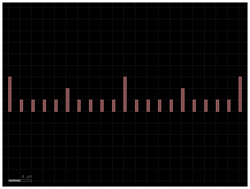
c = litho_ruler()
c.plot()

Lets assume that later on you change the code inside the PCell and want to keep a changelog. You can use the docstring Notes to document any significant changes in the component.
@gf.cell
def litho_ruler(
    height: float = 2,
    width: float = 0.5,
    spacing: float = 2.0,
    scale: tuple[float, ...] = (3, 1, 1, 1, 1, 2, 1, 1, 1, 1),
    num_marks: int = 21,
    layer: LayerSpec = (1, 0),
) -> gf.Component:
    """Ruler structure for lithographic measurement.

    Args:
        height: Height of the ruling marks in um.
        width: Width of the ruling marks in um.
        spacing: Center-to-center spacing of the ruling marks in um.
        scale: Height scale pattern of marks.
        num_marks: Total number of marks to generate.
        layer: Specific layer to put the ruler geometry on.

    Notes:
        5.6.7: distribute across y instead of x.
    """
    D = gf.Component()
    for n in range(num_marks):
        h = height * scale[n % len(scale)]
        ref = D << gf.components.rectangle(size=(width, h), layer=layer)
        ref.rotate(90)

    D.distribute(direction="y", spacing=spacing, separation=False, edge="y")
    D.align(alignment="xmin")
    return D


c = litho_ruler()
c.plot()
