PDK examples#
Different PDKs have different component libraries, design rules and layer stacks (GDS layers, materials and thickness).
When you install a PDK you have to make sure you also installed the correct version of gdsfactory.
Notice that some PDKs may have require different gdsfactory versions.
from collections.abc import Callable
from functools import partial

from pydantic import BaseModel

import gdsfactory as gf
from gdsfactory.add_pins import add_pin_rectangle_inside
from gdsfactory.component import Component
from gdsfactory.config import CONF
from gdsfactory.cross_section import cross_section
from gdsfactory.technology import (
    LayerLevel,
    LayerStack,
    LayerView,
    LayerViews,
    LayerMap,
)
from gdsfactory.typings import Layer
from gdsfactory.config import print_version_pdks, print_version_plugins
from gdsfactory.generic_tech import get_generic_pdk

gf.config.rich_output()
nm = 1e-3
PDK = gf.get_active_pdk()
PDK.name
'generic'
FabA#
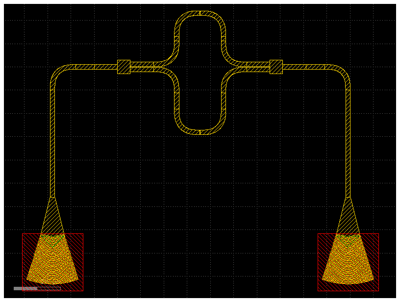
FabA only has one waveguide layer available that is defined in GDS layer (30, 0)
The waveguide traces are 2um wide.
class LayerMapFabA(LayerMap):
    WG: Layer = (34, 0)
    SLAB150: Layer = (2, 0)
    DEVREC: Layer = (68, 0)
    PORT: Layer = (1, 10)
    PORTE: Layer = (1, 11)
    TEXT: Layer = (66, 0)


LAYER = LayerMapFabA()


class FabALayerViews(LayerViews):
    WG: LayerView = LayerView(color="gold")
    SLAB150: LayerView = LayerView(color="red")
    TE: LayerView = LayerView(color="green")


LAYER_VIEWS = FabALayerViews(layer_map=dict(LAYER))


def get_layer_stack_faba(
    thickness_wg: float = 500 * nm, thickness_slab: float = 150 * nm
) -> LayerStack:
    """Returns fabA LayerStack"""

    return LayerStack(
        layers=dict(
            strip=LayerLevel(
                layer=LAYER.WG,
                thickness=thickness_wg,
                zmin=0.0,
                material="si",
            ),
            strip2=LayerLevel(
                layer=LAYER.SLAB150,
                thickness=thickness_slab,
                zmin=0.0,
                material="si",
            ),
        )
    )


LAYER_STACK = get_layer_stack_faba()

WIDTH = 2

# Specify a cross_section to use
strip = partial(gf.cross_section.cross_section, width=WIDTH, layer=LAYER.WG)
xs_sc = strip()

mmi1x2 = partial(
    gf.components.mmi1x2,
    width=WIDTH,
    width_taper=WIDTH,
    width_mmi=3 * WIDTH,
    cross_section=strip,
)

generic_pdk = get_generic_pdk()

PDK = gf.Pdk(
    name="Fab_A",
    cells=dict(mmi1x2=mmi1x2),
    cross_sections=dict(strip=strip, xs_sc=xs_sc),
    layers=dict(LAYER),
    layer_views=LAYER_VIEWS,
    layer_stack=LAYER_STACK,
)
PDK.activate()

PDK_A = PDK

gc = partial(
    gf.components.grating_coupler_elliptical_te, layer=LAYER.WG, cross_section=strip
)

c = gf.components.mzi()
c_gc = gf.routing.add_fiber_array(component=c, grating_coupler=gc, with_loopback=False)
c_gc.plot()

scene = c_gc.to_3d()
scene.show()
FabB#
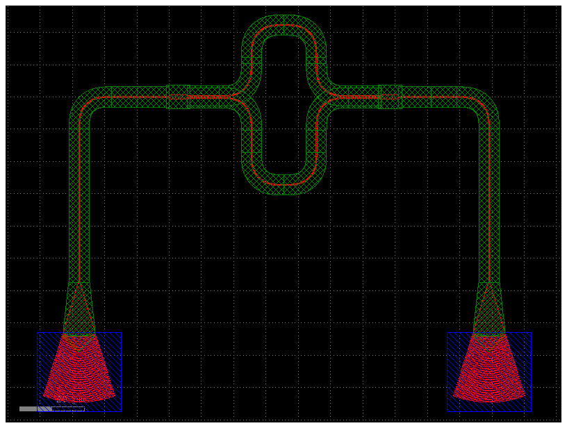
FabB has photonic waveguides that require rectangular cladding layers (bbox_layers)
Lets say that the waveguides are defined in layer (2, 0) and are 0.3um wide, 1um thick
nm = 1e-3


class LayerMapFabB(LayerMap):
    WG: Layer = (2, 0)
    SLAB150: Layer = (3, 0)
    DEVREC: Layer = (68, 0)
    PORT: Layer = (1, 10)
    PORTE: Layer = (1, 11)
    TEXT: Layer = (66, 0)
    DOPING_BLOCK1: Layer = (61, 0)
    DOPING_BLOCK2: Layer = (62, 0)


LAYER = LayerMapFabB()


# The LayerViews class supports grouping LayerViews within each other.
# These groups are maintained when exporting a LayerViews object to a KLayout layer properties (.lyp) file.
class FabBLayerViews(LayerViews):
    WG: LayerView = LayerView(color="red")
    SLAB150: LayerView = LayerView(color="blue")
    TE: LayerView = LayerView(color="green")
    PORT: LayerView = LayerView(color="green", alpha=0)

    class DopingBlockGroup(LayerView):
        DOPING_BLOCK1: LayerView = LayerView(color="green", alpha=0)
        DOPING_BLOCK2: LayerView = LayerView(color="green", alpha=0)

    DopingBlocks: LayerView = DopingBlockGroup()


LAYER_VIEWS = FabBLayerViews(layer_map=LAYER)


def get_layer_stack_fab_b(
    thickness_wg: float = 1000 * nm, thickness_slab: float = 150 * nm
) -> LayerStack:
    """Returns fabA LayerStack."""

    return LayerStack(
        layers=dict(
            strip=LayerLevel(
                layer=LAYER.WG,
                thickness=thickness_wg,
                zmin=0.0,
                material="si",
            ),
            strip2=LayerLevel(
                layer=LAYER.SLAB150,
                thickness=thickness_slab,
                zmin=0.0,
                material="si",
            ),
        )
    )


LAYER_STACK = get_layer_stack_fab_b()


WIDTH = 0.3
BBOX_LAYERS = (LAYER.DOPING_BLOCK1, LAYER.DOPING_BLOCK2)
BBOX_OFFSETS = (3, 3)

# use cladding_layers and cladding_offsets if the foundry prefers conformal blocking doping layers instead of squared
# bbox_layers and bbox_offsets makes rectangular waveguides.
xf_sc = partial(
    gf.cross_section.cross_section,
    width=WIDTH,
    layer=LAYER.WG,
    # bbox_layers=BBOX_LAYERS,
    # bbox_offsets=BBOX_OFFSETS,
    cladding_layers=BBOX_LAYERS,
    cladding_offsets=BBOX_OFFSETS,
)  # cross section factory
xs_sc = xf_sc()  # cross section

straight = partial(gf.components.straight, cross_section=xf_sc)
bend_euler = partial(gf.components.bend_euler, cross_section=xf_sc)
mmi1x2 = partial(
    gf.components.mmi1x2,
    cross_section=xf_sc,
    width=WIDTH,
    width_taper=WIDTH,
    width_mmi=4 * WIDTH,
)
mzi = partial(gf.components.mzi, splitter=mmi1x2, cross_section=xf_sc)
gc = partial(
    gf.components.grating_coupler_elliptical_te, layer=LAYER.WG, cross_section=xf_sc
)

cells = dict(
    gc=gc,
    mzi=mzi,
    mmi1x2=mmi1x2,
    bend_euler=bend_euler,
    straight=straight,
    taper=gf.components.taper,
)
cross_sections = dict(strip=strip)

PDK = gf.Pdk(
    name="fab_b",
    cells=cells,
    cross_sections=cross_sections,
    layers=dict(LAYER),
    layer_views=LAYER_VIEWS,
    layer_stack=LAYER_STACK,
)
PDK.activate()
PDK_B = PDK


c = mzi()
wg_gc = gf.routing.add_fiber_array(
    component=c, grating_coupler=gc, cross_section=xf_sc, with_loopback=False
)
wg_gc.plot()
2025-01-19 23:49:57.702 | WARNING | gdsfactory.pdk:get_cross_section:511 - UserWarning: CrossSection.copy() only modifies the attributes of the first section.

scene = wg_gc.to_3d()
scene.show()
FabC#
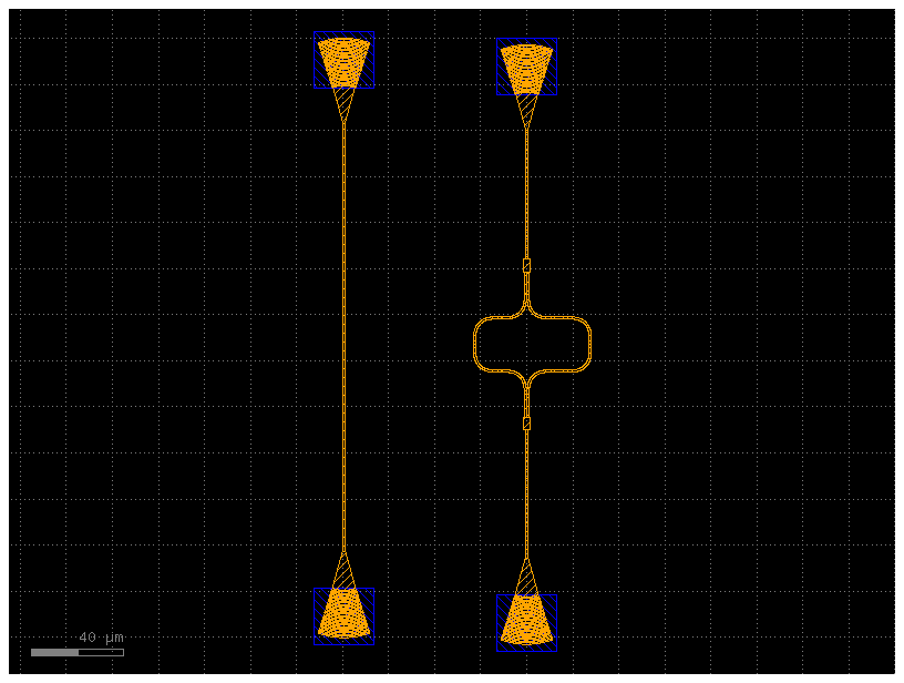
Lets assume that fab C has similar technology to the generic PDK in gdsfactory and that you just want to remap some layers, and adjust the widths.
nm = 1e-3


class LayerMapFabC(LayerMap):
    WG: Layer = (10, 1)
    WG_CLAD: Layer = (10, 2)
    WGN: Layer = (34, 0)
    WGN_CLAD: Layer = (36, 0)
    SLAB150: Layer = (2, 0)
    DEVREC: Layer = (68, 0)
    PORT: Layer = (1, 10)
    PORTE: Layer = (1, 11)
    TEXT: Layer = (66, 0)


LAYER = LayerMapFabC()
WIDTH_NITRIDE_OBAND = 0.9
WIDTH_NITRIDE_CBAND = 1.0
PORT_TYPE_TO_LAYER = dict(optical=(100, 0))


# This is something you usually define in KLayout
class FabCLayerViews(LayerViews):
    WG: LayerView = LayerView(color="black")
    SLAB150: LayerView = LayerView(color="blue")
    WGN: LayerView = LayerView(color="orange")
    WGN_CLAD: LayerView = LayerView(color="blue", alpha=0, visible=False)

    class SimulationGroup(LayerView):
        TE: LayerView = LayerView(color="green")
        PORT: LayerView = LayerView(color="green", alpha=0)

    Simulation: LayerView = SimulationGroup()

    class DopingGroup(LayerView):
        DOPING_BLOCK1: LayerView = LayerView(color="green", alpha=0, visible=False)
        DOPING_BLOCK2: LayerView = LayerView(color="green", alpha=0, visible=False)

    Doping: LayerView = DopingGroup()


LAYER_VIEWS = FabCLayerViews(layer_map=LAYER)


def get_layer_stack_fab_c(
    thickness_wg: float = 350.0 * nm, thickness_clad: float = 3.0
) -> LayerStack:
    """Returns generic LayerStack"""

    return LayerStack(
        layers=dict(
            core=LayerLevel(
                layer=LAYER.WGN,
                thickness=thickness_wg,
                zmin=0,
            ),
            clad=LayerLevel(
                layer=LAYER.WGN_CLAD,
                thickness=thickness_clad,
                zmin=0,
            ),
        )
    )


LAYER_STACK = get_layer_stack_fab_c()

# cross_section constants
bbox_layers = [LAYER.WGN_CLAD]
bbox_offsets = [3]

# Nitride Cband
xs_nc = partial(
    cross_section,
    width=WIDTH_NITRIDE_CBAND,
    layer=LAYER.WGN,
    bbox_layers=bbox_layers,
    bbox_offsets=bbox_offsets,
)
# Nitride Oband
xs_no = partial(
    cross_section,
    width=WIDTH_NITRIDE_OBAND,
    layer=LAYER.WGN,
    bbox_layers=bbox_layers,
    bbox_offsets=bbox_offsets,
)


cross_sections = dict(xs_nc=xs_nc, xs_no=xs_no, strip=xs_nc)

# LEAF cells have pins
mmi1x2_nc = partial(
    gf.components.mmi1x2,
    width=WIDTH_NITRIDE_CBAND,
    cross_section=xs_nc,
)
mmi1x2_no = partial(
    gf.components.mmi1x2,
    width=WIDTH_NITRIDE_OBAND,
    cross_section=xs_no,
)
bend_euler_nc = partial(
    gf.components.bend_euler,
    cross_section=xs_nc,
)
straight_nc = partial(
    gf.components.straight,
    cross_section=xs_nc,
)
bend_euler_no = partial(
    gf.components.bend_euler,
    cross_section=xs_no,
)
straight_no = partial(
    gf.components.straight,
    cross_section=xs_no,
)

gc_nc = partial(
    gf.components.grating_coupler_elliptical_te,
    grating_line_width=0.6,
    layer=LAYER.WGN,
    cross_section=xs_nc,
)

# HIERARCHICAL cells are made of leaf cells
mzi_nc = partial(
    gf.components.mzi,
    cross_section=xs_nc,
    splitter=mmi1x2_nc,
    straight=straight_nc,
    bend=bend_euler_nc,
)
mzi_no = partial(
    gf.components.mzi,
    cross_section=xs_no,
    splitter=mmi1x2_no,
    straight=straight_no,
    bend=bend_euler_no,
)


cells = dict(
    mmi1x2_nc=mmi1x2_nc,
    mmi1x2_no=mmi1x2_no,
    bend_euler_nc=bend_euler_nc,
    bend_euler_no=bend_euler_no,
    straight_nc=straight_nc,
    straight_no=straight_no,
    gc_nc=gc_nc,
    mzi_nc=mzi_nc,
    mzi_no=mzi_no,
)

PDK = gf.Pdk(
    name="fab_c",
    cells=cells,
    cross_sections=cross_sections,
    layers=dict(LAYER),
    layer_views=LAYER_VIEWS,
    layer_stack=LAYER_STACK,
)
PDK_C = PDK
PDK.activate()
LAYER_VIEWS.layer_map.values()
dict_values([(206, 0), (202, 0), (10, 1), (10, 2), (34, 0), (36, 0), (2, 0), (68, 0), (1, 10), (1, 11), (66, 0)])
mzi = mzi_nc()
mzi_gc = gf.routing.add_fiber_single(
    component=mzi,
    grating_coupler=gc_nc,
    cross_section=xs_nc,
    optical_routing_type=1,
    straight=straight_nc,
    bend=bend_euler_nc,
)
mzi_gc.plot()

c = mzi_gc.to_3d()
c.show()
ls = get_layer_stack_fab_c()
Combine multiple PDKs#
You can easily combine multiple PDKs
len(PDK.cells.keys())
9
PDK = gf.Pdk(
    name="fab_c_and_a_combined",
    cells=cells,
    cross_sections=cross_sections,
    layers=dict(LAYER),
    layer_views=LAYER_VIEWS,
    layer_stack=LAYER_STACK,
    base_pdks=[PDK_C, PDK_A],
)
PDK.activate()
len(PDK.cells.keys())
10
PDK = gf.Pdk(
    name="fab_c_and_generic_combined",
    cells=cells,
    cross_sections=cross_sections,
    layers=dict(LAYER),
    layer_views=LAYER_VIEWS,
    layer_stack=LAYER_STACK,
    base_pdks=[PDK_C, get_generic_pdk()],
)
PDK.activate()
len(PDK.cells.keys())
296
