KCLayout — layout context and PDK
KCLayout is the root container for everything kfactory manages: layers, cells,
factories, enclosures, and cross-sections. It wraps a KLayout kdb.Layout object
and adds kfactory-specific tracking on top.
Key facts:
kf.kclis the default, module-levelKCLayout. Most single-PDK workflows only ever use this one object.- You can create additional
KCLayoutinstances to model a second PDK or a cell library — cells from any layout can be instantiated inside any other. - The
dbuattribute controls the database unit (grid size in µm). The default is0.001(1 nm grid). Changing it on an empty layout is safe; changing it after cells have been added causes geometry to shift. - The
factoriesdict maps string names to decorated cell functions registered on this layout. Callingkcl.factories["straight"](...)is equivalent to calling the underlying function directly.
Setup: layers
Each notebook defines its own layer set. The kf.kcl.infos = L line makes the
default layout aware of these layers so helpers like find_layer work.
import kfactory as kf


class LAYER(kf.LayerInfos):
    WG: kf.kdb.LayerInfo = kf.kdb.LayerInfo(1, 0)
    WGEX: kf.kdb.LayerInfo = kf.kdb.LayerInfo(2, 0)
    CLAD: kf.kdb.LayerInfo = kf.kdb.LayerInfo(4, 0)
    FLOORPLAN: kf.kdb.LayerInfo = kf.kdb.LayerInfo(10, 0)


L = LAYER()
kf.kcl.infos = L
The default layout: kf.kcl
kf.kcl is always available after import kfactory as kf. It holds the global
namespace of cells.
# Name and grid size of the default layout
print(f"name : {kf.kcl.name}")
print(f"dbu  : {kf.kcl.dbu} µm  ({kf.kcl.dbu * 1000:.0f} nm grid)")
name : DEFAULT
dbu  : 0.001 µm  (1 nm grid)
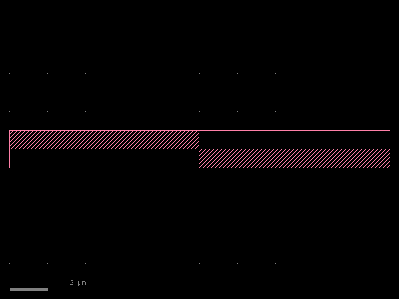
# Create a straight waveguide in the default layout
s = kf.cells.straight.straight(width=1, length=10, layer=L.WG)
s
# The layout now contains one registered KCell
kf.kcl.kcells
KCells(DEFAULT, n=0)
Creating a second layout (second PDK)
Pass a name string to KCLayout(...). You can also set a different dbu to
simulate a PDK with a coarser grid (e.g. 5 nm instead of 1 nm).
kcl2 = kf.KCLayout("DEMO_PDK", infos=LAYER)
kcl2.dbu = 0.005  # 5 nm grid
print(f"name : {kcl2.name}")
print(f"dbu  : {kcl2.dbu} µm  ({kcl2.dbu * 1000:.0f} nm grid)")
name : DEMO_PDK
dbu  : 0.005 µm  (5 nm grid)
# The new layout starts empty
kcl2.kcells
KCells(DEMO_PDK, n=0)
Registering a factory on a custom layout
straight_dbu_factory returns a cell function that is pre-bound to kcl2.
After registration, the factory is accessible by name via kcl2.factories.
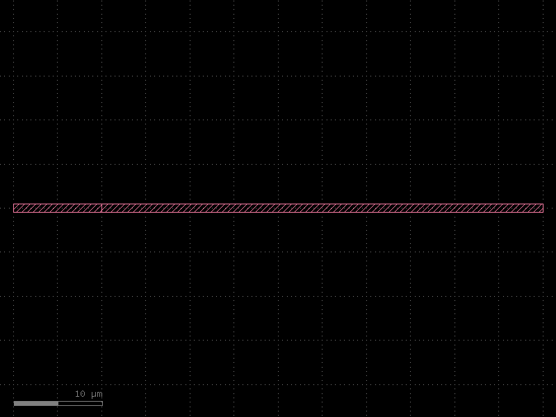
sf2 = kf.factories.straight.straight_dbu_factory(kcl=kcl2)

# Call the factory directly …
s2 = kcl2.factories["straight"](length=10_000, width=200, layer=L.WG)
s2.settings
KCellSettings(width=200, length=10000, layer=WG (1/0), enclosure=None)
DBU vs µm dimensions across layouts
The same physical width (1 µm) occupies different numbers of database units
depending on the grid size. The dbbox() method always returns µm regardless
of dbu.
# Default layout: 1 nm grid  → 1 µm = 1000 dbu
print("--- default kcl (1 nm grid) ---")
print(f"  height dbu : {s.bbox().height()}")
print(f"  height µm  : {s.dbbox().height()}")
print(f"  width  dbu : {s.bbox().width()}")
print(f"  width  µm  : {s.dbbox().width()}")

# DEMO_PDK: 5 nm grid  → 1 µm = 200 dbu
print("--- DEMO_PDK (5 nm grid) ---")
print(f"  height dbu : {s2.bbox().height()}")
print(f"  height µm  : {s2.dbbox().height()}")
print(f"  width  dbu : {s2.bbox().width()}")
print(f"  width  µm  : {s2.dbbox().width()}")
--- default kcl (1 nm grid) ---
  height dbu : 1000
  height µm  : 1.0
  width  dbu : 10000
  width  µm  : 10.0
--- DEMO_PDK (5 nm grid) ---
  height dbu : 200
  height µm  : 1.0
  width  dbu : 10000
  width  µm  : 50.0
Port widths follow the same rule — ports.print() shows DBU values by default;
pass unit="um" to see physical (µm) values instead.
print("=== ports in DBU ===")
s.ports.print()
s2.ports.print()

print("\n=== ports in µm ===")
s.ports.print(unit="um")
s2.ports.print(unit="um")
=== ports in DBU ===
┏━━━━━━┳━━━━━━━┳━━━━━━━━━━┳━━━━━━━━━┳━━━━━━━━┳━━━┳━━━━━━━┳━━━━━━━━┳━━━━━━┓
┃[1m [0m[1mName[0m[1m [0m┃[1m [0m[1mWidth[0m[1m [0m┃[1m [0m[1mLayer [0m[1m [0m┃[1m [0m[1mType [0m[1m [0m┃[1m [0m[1mX [0m[1m [0m┃[1m [0m[1mY[0m[1m [0m┃[1m [0m[1mAngle[0m[1m [0m┃[1m [0m[1mMirror[0m[1m [0m┃[1m [0m[1mInfo[0m[1m [0m┃
┡━━━━━━╇━━━━━━━╇━━━━━━━━━━╇━━━━━━━━━╇━━━━━━━━╇━━━╇━━━━━━━╇━━━━━━━━╇━━━━━━┩
│ o1 │ 1_000 │ WG (1/0) │ optical │ 0 │ 0 │ 2 │ False │ [1m{[0m[1m}[0m │
├──────┼───────┼──────────┼─────────┼────────┼───┼───────┼────────┼──────┤
│ o2 │ 1_000 │ WG (1/0) │ optical │ 10_000 │ 0 │ 0 │ False │ [1m{[0m[1m}[0m │
└──────┴───────┴──────────┴─────────┴────────┴───┴───────┴────────┴──────┘
┏━━━━━━┳━━━━━━━┳━━━━━━━━━━┳━━━━━━━━━┳━━━━━━━━┳━━━┳━━━━━━━┳━━━━━━━━┳━━━━━━┓
┃[1m [0m[1mName[0m[1m [0m┃[1m [0m[1mWidth[0m[1m [0m┃[1m [0m[1mLayer [0m[1m [0m┃[1m [0m[1mType [0m[1m [0m┃[1m [0m[1mX [0m[1m [0m┃[1m [0m[1mY[0m[1m [0m┃[1m [0m[1mAngle[0m[1m [0m┃[1m [0m[1mMirror[0m[1m [0m┃[1m [0m[1mInfo[0m[1m [0m┃
┡━━━━━━╇━━━━━━━╇━━━━━━━━━━╇━━━━━━━━━╇━━━━━━━━╇━━━╇━━━━━━━╇━━━━━━━━╇━━━━━━┩
│ o1 │ 200 │ WG (1/0) │ optical │ 0 │ 0 │ 2 │ False │ [1m{[0m[1m}[0m │
├──────┼───────┼──────────┼─────────┼────────┼───┼───────┼────────┼──────┤
│ o2 │ 200 │ WG (1/0) │ optical │ 10_000 │ 0 │ 0 │ False │ [1m{[0m[1m}[0m │
└──────┴───────┴──────────┴─────────┴────────┴───┴───────┴────────┴──────┘
=== ports in µm ===
┏━━━━━━┳━━━━━━━┳━━━━━━━━━━┳━━━━━━━━━┳━━━━━━┳━━━━━┳━━━━━━━┳━━━━━━━━┳━━━━━━┓
┃[1m [0m[1mName[0m[1m [0m┃[1m [0m[1mWidth[0m[1m [0m┃[1m [0m[1mLayer [0m[1m [0m┃[1m [0m[1mType [0m[1m [0m┃[1m [0m[1mX [0m[1m [0m┃[1m [0m[1mY [0m[1m [0m┃[1m [0m[1mAngle[0m[1m [0m┃[1m [0m[1mMirror[0m[1m [0m┃[1m [0m[1mInfo[0m[1m [0m┃
┡━━━━━━╇━━━━━━━╇━━━━━━━━━━╇━━━━━━━━━╇━━━━━━╇━━━━━╇━━━━━━━╇━━━━━━━━╇━━━━━━┩
│ o1 │ 1.0 │ WG (1/0) │ optical │ 0.0 │ 0.0 │ 180.0 │ False │ [1m{[0m[1m}[0m │
├──────┼───────┼──────────┼─────────┼──────┼─────┼───────┼────────┼──────┤
│ o2 │ 1.0 │ WG (1/0) │ optical │ 10.0 │ 0.0 │ 0.0 │ False │ [1m{[0m[1m}[0m │
└──────┴───────┴──────────┴─────────┴──────┴─────┴───────┴────────┴──────┘
┏━━━━━━┳━━━━━━━┳━━━━━━━━━━┳━━━━━━━━━┳━━━━━━┳━━━━━┳━━━━━━━┳━━━━━━━━┳━━━━━━┓
┃[1m [0m[1mName[0m[1m [0m┃[1m [0m[1mWidth[0m[1m [0m┃[1m [0m[1mLayer [0m[1m [0m┃[1m [0m[1mType [0m[1m [0m┃[1m [0m[1mX [0m[1m [0m┃[1m [0m[1mY [0m[1m [0m┃[1m [0m[1mAngle[0m[1m [0m┃[1m [0m[1mMirror[0m[1m [0m┃[1m [0m[1mInfo[0m[1m [0m┃
┡━━━━━━╇━━━━━━━╇━━━━━━━━━━╇━━━━━━━━━╇━━━━━━╇━━━━━╇━━━━━━━╇━━━━━━━━╇━━━━━━┩
│ o1 │ 1.0 │ WG (1/0) │ optical │ 0.0 │ 0.0 │ 180.0 │ False │ [1m{[0m[1m}[0m │
├──────┼───────┼──────────┼─────────┼──────┼─────┼───────┼────────┼──────┤
│ o2 │ 1.0 │ WG (1/0) │ optical │ 50.0 │ 0.0 │ 0.0 │ False │ [1m{[0m[1m}[0m │
└──────┴───────┴──────────┴─────────┴──────┴─────┴───────┴────────┴──────┘
Mixing cells from different layouts
Cells from any KCLayout can be instantiated inside a cell belonging to another
layout. kfactory copies the referenced cell's geometry transparently.
c = kf.kcl.kcell("mixed_pdks")
si_default = c << s  # instance of the 1 nm-grid straight
si_demo = c << s2  # instance of the 5 nm-grid straight

# Connect port o1 of the demo cell to port o2 of the default cell
si_demo.connect("o1", si_default, "o2")
c
Saving and loading GDS files
KCLayout.write() serialises the layout (and its cell metadata) to a GDS/OASIS
file. KCLayout.read() loads it back.
import tempfile
from pathlib import Path

with tempfile.TemporaryDirectory() as tmp:
    gds_path = Path(tmp) / "demo.gds"
    kf.kcl.write(gds_path)
    print(f"written: {gds_path.stat().st_size} bytes")

    # Load into a fresh layout to verify round-trip
    kcl3 = kf.KCLayout("LOADED")
    kcl3.read(gds_path, register_cells=True)
    print(f"cells read back: {list(kcl3.kcells.keys())[:5]}")
written: 1332 bytes
cells read back: [1, 0, 2]
Key attributes at a glance
| Attribute / method | Type | Description |
|---|---|---|
kcl.name |
str |
Layout identifier |
kcl.dbu |
float |
Grid size in µm (e.g. 0.001 = 1 nm) |
kcl.layout |
kdb.Layout |
Underlying KLayout object |
kcl.kcells |
KCells |
Mapping of cell index → KCell |
kcl.infos |
LayerInfos |
Layer definitions |
kcl.factories |
Factories |
Registered cell-factory functions |
kcl.kcell(name) |
KCell |
Create a new, empty cell |
kcl.read(path) |
— | Load GDS/OASIS file |
kcl.write(path) |
— | Save GDS/OASIS file |
See Also
| Topic | Where |
|---|---|
| Building a full PDK with a custom KCLayout | PDK: Creating a PDK |
| Session save/load to speed up rebuilds | Utilities: Session Cache |
| GDS/OASIS regression testing | Utilities: Regression Testing |
| Layer definitions and LayerInfos | Core Concepts: Layers |