
COMSOL Full-Wave Simulation of a Coupled Quarter-Wave Resonator#
Required extras
Needs the comsol extra (uv sync --extra comsol), which installs gplugins[comsol] and
MPh. The layout, plotting, and result helpers come from gplugins, so every cell needs the extra.
COMSOL, its license, the RF Module, and the Design Module CAD kernel that ProjectToFaces needs
are separate. See the extras reference.
The shortest path from a QPDK layout to a driven COMSOL result: build a coupled quarter-wave resonator, put its metal into a COMSOL sheet model, add CPW ports and a frequency study, run one adaptive driven sweep about the resonance, then solve once at its fitted minimum to export a field on a cut plane.
What is being modelled#
A QPDK quarter_wave_resonator_coupled(): a meandering coplanar-waveguide (CPW)
resonator beside a straight feedline, the standard hanger geometry for reading out superconducting
qubits [GFB+08], whose resonance is one of the degrees of
freedom circuit QED reads a qubit through [BGGW21]. The end
nearest the feedline is open and the far end shorted, so the line resonates at an odd
multiple of \(\lambda/4\) [MP12], and the coupling capacitor loads
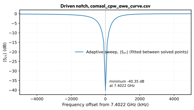
the feedline into a notch in \(|S_{21}|\).
Reading the numbers on this page
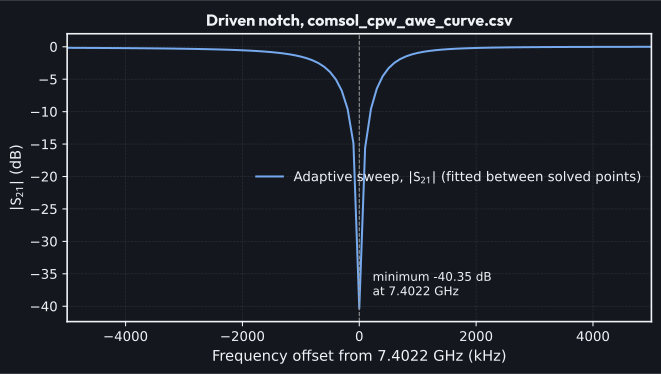
The saved outputs come from a licensed run on one mesh. Only the frequencies COMSOL actually solved are independent results; the rest of the sweep is a rational fit, so the curve locates the notch but does not resolve it. PEC metal carries no conductor loss or kinetic inductance, nothing here is shown to be mesh independent, and a fresh run on another mesh or enclosure will not reproduce these numbers exactly.
References:
Setup and imports#
Settings#
The sweep is centred on the resonance the saved run found near 7.4022 GHz. RUN_COMSOL stays
False, so no solve starts by accident; the result cells below read whatever export is on disk.
Build the ported layout#
The resonator is built with an explicit CPW cross-section, since the centre width and gap are reused when describing the ports. Both feeds are extended with straight CPW so the ports land on clean cross sections.
cross_section = coplanar_waveguide(width=CPW_WIDTH_UM, gap=CPW_GAP_UM)

resonator = quarter_wave_resonator_coupled(
    length=4000.0,
    meanders=4,
    cross_section=cross_section,
    cross_section_non_resonator=cross_section,
    coupling_straight_length=200.0,
    coupling_gap=20.0,
)

component = gf.Component(name="comsol_cpw_resonator")
component << resonator

left_straight = component << gf.components.straight(
    length=LEFT_EXTENSION_UM, cross_section=cross_section
)
right_straight = component << gf.components.straight(
    length=RIGHT_EXTENSION_UM, cross_section=cross_section
)
left_straight.connect("o2", resonator.ports["coupling_o1"])
right_straight.connect("o1", resonator.ports["coupling_o2"])
component.add_port("input", port=left_straight.ports["o1"])
component.add_port("output", port=right_straight.ports["o2"])
DPort(self.name='output', self.width=10.0, trans=r0 *1 2200,0, layer=M1_DRAW (1/0), port_type=optical)
layout = prepare_comsol_layout(
    component,
    feed_ports=("input", "output"),
    ground_margin=GROUND_MARGIN_UM,
    crop_to_feed_ports=True,
)
print(
    f"Metal polygons: {len(layout.polygons)}, prepared bounding box (µm): {layout.bbox}"
)
Metal polygons: 3, prepared bounding box (µm): ComsolBoundingBox(xmin=-1320.0, ymin=-2041.0, xmax=2200.0, ymax=1211.0)
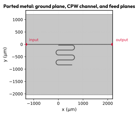
One ground plane with a single hole: the CPW channel, carrying the centre strip, both etch gaps, and
the surrounding ground. Keeping the hole is what makes ProjectToFaces necessary, so the etched
region stays open in the sheet.
fig, ax = plt.subplots(figsize=(7, 4))
draw_layout_polygons(ax, layout.polygons)
for feed in layout.feed_ports:
    ax.plot(*feed.center, marker="o", color="crimson", markersize=6, zorder=4)
    ax.annotate(
        feed.name,
        feed.center,
        textcoords="offset points",
        xytext=(8, 8),
        fontsize=9,
        color="crimson",
    )
ax.set_aspect("equal")
ax.set_xlabel("x (µm)")
ax.set_ylabel("y (µm)")
ax.set_title("Ported metal: ground plane, CPW channel, and feed planes")
plt.tight_layout()
plt.show()
findfont: Failed to find font weight bold, now using 400.
Build and solve the driven model#
gplugins.comsol.COMSOL builds the air, silicon, and metal sheet, and
add_cpw_rf_study adds PEC metal, two CPW ports
with their boundary mode analysis steps, and a frequency study. The meander edges then get a
tighter absolute element size before the adaptive sweep. A direct solve at the fitted minimum
supplies the field export. The substrate thickness and the silicon permittivity are not set here: they
come from the Substrate level of the PDK layer stack and its material in qpdk.tech.material_properties,
the same numbers the analytical CPW model uses. The metal is a zero-thickness sheet, so the M1 film
thickness does not enter. Only the air height is a choice of this simulation domain.
The step below is off by default. Run it on a licensed machine to build, mesh, solve, save an
.mph, write the curve CSV, and export the field.
The licensed solve is off by default. Set RUN_COMSOL = True on a machine with COMSOL and its license to build, mesh, solve, and export the driven model; the cells below then read those exports from MODEL_DIR.
Saved S21 curve#
The curve below reads an export from the licensed step or a saved run. Its line is the adaptive sweep’s rational fit: most rows are interpolation between the frequencies COMSOL actually solved, so the curve locates the notch but does not resolve it. The run that produced it was more controlled than a fresh single solve, and a rerun on another mesh or machine will differ in detail.
curve_path = result_file(RESULTS_DIR, AWE_CURVE_CSV)
if curve_path is None and RESULTS_DIR is not None:
    # Older runs tagged the curve with their run ID instead of the fixed name.
    tagged = sorted(
        RESULTS_DIR.glob("comsol_cpw_awe_curve-*.csv"),
        key=lambda path: path.stat().st_mtime,
    )
    curve_path = tagged[-1] if tagged else None

if curve_path is None:
    print(explain_missing_results(RESULTS_DIR, AWE_CURVE_CSV))
else:
    curve = np.atleast_1d(np.genfromtxt(curve_path, delimiter=",", names=True))
    frequency_ghz = np.asarray(curve["frequency_ghz"], dtype=float)
    s21_db = np.asarray(curve["s21_db"], dtype=float)
    minimum_index = int(np.argmin(s21_db))
    offset_khz = (frequency_ghz - SWEEP_CENTER_GHZ) * 1e6

    fig, ax = plt.subplots(figsize=(7, 4))
    ax.plot(
        offset_khz,
        s21_db,
        color="C0",
        label=r"Adaptive sweep, $|S_{21}|$ (fitted between solved points)",
    )
    ax.axvline(0.0, color="0.6", linewidth=0.8, linestyle="--")
    ax.annotate(
        f"minimum {s21_db[minimum_index]:+.2f} dB\nat {frequency_ghz[minimum_index]:.4f} GHz",
        (offset_khz[minimum_index], s21_db[minimum_index]),
        textcoords="offset points",
        xytext=(10, 10),
        fontsize=9,
    )
    ax.set_xlabel(f"Frequency offset from {SWEEP_CENTER_GHZ:g} GHz (kHz)")
    ax.set_ylabel(r"$|S_{21}|$ (dB)")
    ax.set_title(f"Driven notch, {curve_path.name}")
    ax.grid(True, alpha=0.3)
    ax.legend()
    plt.tight_layout()
    plt.show()
Saved driven field map#
emw.normE on a cut plane 1 µm above the metal, from a direct solve at the fitted minimum. The export’s header names
the frequency the field was solved at, so the title says which solution it shows. The amplitude
follows the solver’s drive normalization, so the colour scale gives relative shape rather than a
field strength at a stated input power. The figure crops to the coupling section, the meander, and
the feedline, and for display only draws a fixed-stride subset of the cropped nodes.
field_path = result_file(RESULTS_DIR, DRIVEN_FIELD_TXT)
if field_path is None:
    print(explain_missing_results(RESULTS_DIR, DRIVEN_FIELD_TXT))
else:
    field_frequency_ghz = exported_frequency_ghz(field_path, bare_unit="GHz")
    draw_cut_plane_field(
        field_path,
        f"Driven $|\\mathbf{{E}}|$ at {field_frequency_ghz:g} GHz, z = 1 µm"
        if field_frequency_ghz is not None
        else "Driven $|\\mathbf{E}|$ at z = 1 µm",
        view_um=FIELD_VIEW_UM,
        stride=4,
        contour_levels=30,
    )
Field nodes: 55395 of 75313 inside the view; 13849 drawn at stride 4; range 1.04e+03 to 3.09e+08 V/m, 1st to 99th percentile 2.99e+04 to 2.19e+08 V/m
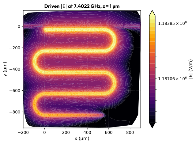
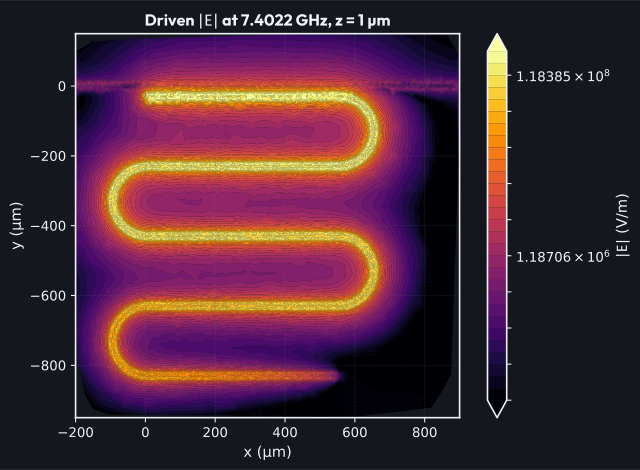
The field sits on the meander and is weak on the feedline, which is what a mode localised on the resonator looks like. Localisation is not the quarter-wave condition, and one cut plane from one solve is a consistency check on the field, not a convergence result.
Summary#
A scripted path from a QPDK layout through a sheet model to a driven \(S_{21}\) notch and a field map, all on one mesh. The notch depth comes from the coupling plus whatever loss the model carries, and PEC adds no conductor or dielectric loss. This is a demonstration of the workflow, not a converged model or a device prediction.
Next steps#
Refine the mesh and check whether the notch frequency and depth move.
Fit a quality factor from the notch width, after confirming the sweep resolves it.
Replace the outer PEC walls with scattering boundaries, and PEC with a surface-impedance condition.
References#
Alexandre Blais, Arne L. Grimsmo, S. M. Girvin, and Andreas Wallraff. Circuit quantum electrodynamics. Reviews of Modern Physics, 93(2):025005, May 2021. doi:10.1103/RevModPhys.93.025005.
M. Göppl, A. Fragner, M. Baur, R. Bianchetti, S. Filipp, J. M. Fink, P. J. Leek, G. Puebla, L. Steffen, and A. Wallraff. Coplanar waveguide resonators for circuit quantum electrodynamics. Journal of Applied Physics, 104(11):113904, December 2008. doi:10.1063/1.3010859.
David M. Pozar. Microwave Engineering. John Wiley & Sons, Inc., 4 edition, 2012. ISBN 978-0-470-63155-3.