
COMSOL transmon capacitance and field#
Required extras
This notebook needs the comsol extra (uv sync --extra comsol). It installs gplugins[comsol], which
brings the COMSOL model builder and MPh, the Python client for COMSOL. It does not install COMSOL or a
license, so the build and solve cells need a local installation and cannot run on Colab. See the extras reference.
This tutorial walks the path end to end: build a QPDK double-pad transmon, copy it without the Josephson junction layers, extract the metal layout, run a stationary Electrostatics solve on a COMSOL sheet model, and read the capacitance and the potential and field the solve stores. The figures are saved cell outputs of licensed solves; without a license the COMSOL cells are skipped and the result cells say so.
What is modelled, and what is solved#
The device is a QPDK double_pad_transmon_with_bbox(): two pads joined
only through the Josephson junction, with a SQUID loop at the centre, so the qubit frequency follows
from \(E_\text{J}\) and \(E_\text{C} = e^2 / 2C\) [KYG+07]. The sheet
model cannot represent the junction overlap or its barrier, so the extraction uses an EM-only copy with
the junction layers removed: the SQUID loop and its leads are absent from the solved geometry.
The solve adds Electrostatics, not electromagnetic waves, and returns es.C11, the driven pad’s
capacitance to the grounded rest of the chip, plus es.intWe, which agree through
\(2 W_\text{e} / V^2 = C_{11}\) [MP12]. It is a quasi-static extraction,
with no Josephson inductance and no resonance solved.
        flowchart TB
    A["Transmon cell"] --> B["EM-only copy"] --> C["Extracted layout"] --> D["Sheet model"] --> E["Electrostatics"] --> F["Mesh, stationary solve"] --> G["C11, intWe, V, normE"]
Reading the numbers on this page
The values come from a licensed electrostatic solve, but they are not a validated device prediction: the SQUID loop and leads are absent, and \(C_{11}\) is a one-terminal value, the driven pad against the grounded chip, not the two-pad differential capacitance that sets \(E_\text{C}\) [BGGW21]. Nothing here is a transmon eigenmode or an \(f_{01}\).
References:
QPDK transmon physics and the double-pad cell:
double_pad_transmon_with_bbox()
Setup and imports#
Build the transmon cell and an EM-only copy#
prepare_comsol_layout rejects geometry on layers it does not model, the junction layers among them. The
cell is copied and JJ_AREA and JJ_PATCH removed, leaving M1_DRAW and the M1_ETCH mask.
component = double_pad_transmon_with_bbox(bbox_extension=200.0)

junction_port = component.ports["junction"]
junction_x, junction_y = junction_port.center
JUNCTION_CENTER_UM = (junction_x, junction_y)

em_component = component.copy()
em_component.remove_layers(layers=[LAYER.JJ_AREA, LAYER.JJ_PATCH])

print(f"Component: {component.name}")
print(f"Bounding box (µm): {component.bbox()}")
print(f"Junction site: center={JUNCTION_CENTER_UM} µm")
print(f"Layers kept:   {sorted(em_component.layers)}")
print("JJ_AREA/JJ_PATCH removed; M1_DRAW and M1_ETCH remain.")
Component: double_pad_transmon_with_bbox_BE200_PS250_400_PG15_JSsq_c3fdad3b
Bounding box (µm): (-457.5,-400;457.5,400)
Junction site: center=(0.0, 0.0) µm
Layers kept:   [(1, 0), (1, 1)]
JJ_AREA/JJ_PATCH removed; M1_DRAW and M1_ETCH remain.
Extract the COMSOL layout#
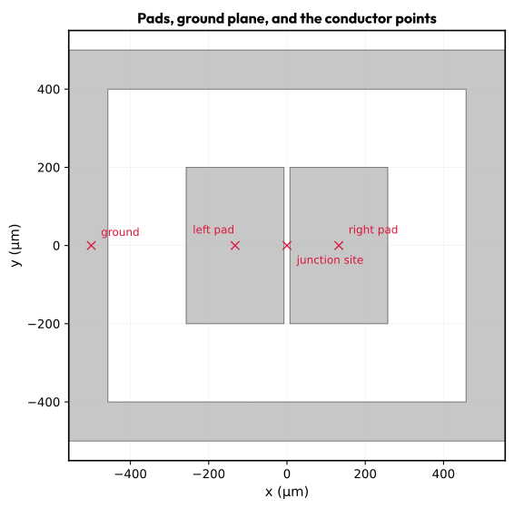
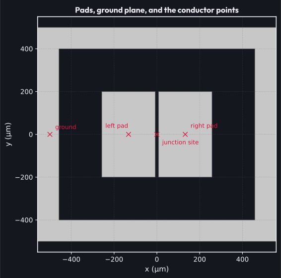
The pads are not transmission-line ports, so no feed ports are requested. The etched moat is a hole in the ground-plane polygon; the pads sit inside it as separate polygons.
layout = prepare_comsol_layout(em_component, feed_ports=None, ground_margin=100.0)

print(f"Metal polygons: {len(layout.polygons)}")
print(f"Feed ports:     {layout.feed_ports}")
print(f"Prepared bbox (µm): {layout.bbox}")

# Three conductor faces: the two pads and the ground plane. Each point below
# sits well inside its metal region so the face selection resolves to exactly
# one face, which the study builder checks before adding the terminals.
LEFT_PAD_POINT = (-132.5, 0.0)
RIGHT_PAD_POINT = (132.5, 0.0)
GROUND_POINT = (-500.0, 0.0)

# The study names one face selection per conductor after these tags, so the mesh
# sizes and the terminal and ground arguments below can name a face by tag.
PAD_L_SELECTION = "pad_l"
PAD_R_SELECTION = "pad_r"
GROUND_SELECTION = "gnd"
CONDUCTORS = (
    (PAD_L_SELECTION, LEFT_PAD_POINT),
    (PAD_R_SELECTION, RIGHT_PAD_POINT),
    (GROUND_SELECTION, GROUND_POINT),
)
Metal polygons: 3
Feed ports:     ()
Prepared bbox (µm): ComsolBoundingBox(xmin=-557.5, ymin=-500.0, xmax=557.5, ymax=500.0)
fig, ax = plt.subplots(figsize=(6, 6))
draw_layout_polygons(ax, layout.polygons)
for point, label, offset in (
    (LEFT_PAD_POINT, "left pad", (-35, 10)),
    (RIGHT_PAD_POINT, "right pad", (8, 10)),
    (GROUND_POINT, "ground", (8, 8)),
    (JUNCTION_CENTER_UM, "junction site", (8, -15)),
):
    ax.plot(*point, marker="x", color="crimson", markersize=7, zorder=4)
    ax.annotate(
        label,
        point,
        textcoords="offset points",
        xytext=offset,
        fontsize=9,
        color="crimson",
    )
ax.set_aspect("equal")
ax.set_xlabel("x (µm)")
ax.set_ylabel("y (µm)")
ax.set_title("Pads, ground plane, and the conductor points")
plt.tight_layout()
plt.show()
findfont: Failed to find font weight bold, now using 400.
Build the COMSOL model and capacitance study#
Three calls configure the model: gplugins.comsol.COMSOL.create_sheet makes the
air and silicon blocks meeting at \(z = 0\), imprints the layout metal on that interface as faces, and
assigns materials;
add_capacitance_study picks the pad and ground faces from
the points above, drives the left pad, grounds the right pad and the ground plane, and adds the mesh and a
stationary study; and pin_absolute_mesh_sizes reruns that
mesh with absolute element sizes in micrometres, so the near-metal resolution does not move with the
domain.
The silicon thickness and permittivity are read from the Substrate level of the PDK layer stack and its
material in qpdk.tech.material_properties, so they match every other QPDK simulation. The metal is a
zero-thickness sheet, so the M1 film thickness does not enter. The air height and lateral margin only size
the simulation domain.
RUN_COMSOL is False by default, so a documentation build without a license skips all of this and the
result cells below read saved exports instead. Set it to True on a licensed machine to solve and export.
The constants are the configuration the saved exports were produced at.
RUN_COMSOL = False
MODEL_DIR = Path.home() / "comsol_models"
RESULTS_DIR_ENV = "QPDK_COMSOL_RESULTS_DIR"
# The environment variable wins when it is set and non-empty, so a run without a
# license can still read a licensed run's exports.
_results_from_environment = os.environ.get(RESULTS_DIR_ENV)
RESULTS_DIR: Path | None = (
    Path(_results_from_environment).expanduser()
    if _results_from_environment
    else MODEL_DIR
    if RUN_COMSOL
    else None
)

MODEL_PATH = MODEL_DIR / "comsol_qubit_capacitance.mph"
METRICS_JSON = "comsol_qubit_metrics.json"
FIELD_TXT = "comsol_qubit_field.txt"
CORES = 4
VOLTAGE_V = 1.0

# The substrate thickness comes from the PDK layer stack and the permittivities
# from `qpdk.simulation.comsol`; the air height and lateral margin size the
# simulation domain, in µm.
SUBSTRATE_THICKNESS_UM = LAYER_STACK.layers["Substrate"].thickness
AIR_HEIGHT_UM = 1600.0
LATERAL_MARGIN_UM = 8000.0
# Element size COMSOL's physics-controlled build starts from. The pinned sizes
# below replace it, so it only sets the sizing the sequence is materialised with.
BASE_MESH_SIZE = 2
GLOBAL_HMAX_UM = 1000.0
GLOBAL_HMIN_UM = 2.0
HGRAD = 1.4
HCURVE = 0.5
HNARROW = 0.7
# Near-metal element sizes (hmax, hmin) in µm, one per conductor face. Each hmin
# is a tenth of its hmax.
NEAR_METAL = "0.625/1.25"
PAD_HMAX_UM, PAD_HMIN_UM = 0.625, 0.0625
GROUND_HMAX_UM, GROUND_HMIN_UM = 1.25, 0.125
Solve, save, and export#
One licensed cell: build, mesh, and solve, then save the model, write comsol_qubit_metrics.json, and
export \(V\) and es.normE on a cut plane at \(z = 1\,\text{µm}\) into comsol_qubit_field.txt through
COMSOL’s Java Data export.
model = None

if RUN_COMSOL:
    MODEL_DIR.mkdir(parents=True, exist_ok=True)
    client = mph.start(cores=CORES)
    model = COMSOL.create_sheet(
        client,
        layout,
        name="QPDK Double-Pad Transmon",
        substrate_thickness_um=SUBSTRATE_THICKNESS_UM,
        air_height_um=AIR_HEIGHT_UM,
        lateral_margin_um=LATERAL_MARGIN_UM,
        silicon_relative_permittivity=SILICON_RELATIVE_PERMITTIVITY,
        air_relative_permittivity=AIR_RELATIVE_PERMITTIVITY,
    ).add_capacitance_study(
        conductors=CONDUCTORS,
        terminal=PAD_L_SELECTION,
        grounds=(PAD_R_SELECTION, GROUND_SELECTION),
        voltage_v=VOLTAGE_V,
        mesh_size=BASE_MESH_SIZE,
    )
    element_count = model.pin_absolute_mesh_sizes(
        global_hmax_um=GLOBAL_HMAX_UM,
        global_hmin_um=GLOBAL_HMIN_UM,
        face_sizes={
            PAD_L_SELECTION: (PAD_HMAX_UM, PAD_HMIN_UM),
            PAD_R_SELECTION: (PAD_HMAX_UM, PAD_HMIN_UM),
            GROUND_SELECTION: (GROUND_HMAX_UM, GROUND_HMIN_UM),
        },
        hgrad=HGRAD,
        hcurve=HCURVE,
        hnarrow=HNARROW,
    )
    model.java.study("std1").run()
    for problem in model.problems():
        print(f"The solve reports: {problem}")

    (MODEL_DIR / FIELD_TXT).unlink(missing_ok=True)
    model.save(MODEL_PATH)

    capacitance_f = float(np.asarray(model.evaluate("es.C11")))
    stored_energy_j = float(np.asarray(model.evaluate("es.intWe")))
    print(f"es.C11 = {capacitance_f:.6e} F")
    print(f"es.intWe = {stored_energy_j:.6e} J")
    print(f"2*intWe/V^2 = {2.0 * stored_energy_j / VOLTAGE_V**2:.6e} F")
    print(f"Mesh elements = {element_count}")
    print(f"Saved model to {MODEL_PATH}")

    write_json_atomically(
        MODEL_DIR / METRICS_JSON,
        {
            "capacitance_f": capacitance_f,
            "stored_energy_j": stored_energy_j,
            "voltage_v": VOLTAGE_V,
            "solver": "COMSOL Multiphysics",
            "study": "Electrostatics stationary",
            "mesh": "absolute element sizes, physics-controlled sizing replaced",
            "element_count": element_count,
            "near_metal": NEAR_METAL,
            "lateral_margin_um": LATERAL_MARGIN_UM,
            "substrate_thickness_um": SUBSTRATE_THICKNESS_UM,
            "air_height_um": AIR_HEIGHT_UM,
            "silicon_relative_permittivity": SILICON_RELATIVE_PERMITTIVITY,
        },
    )

    result = model.java.result()
    # Rerunning this cell must not collide with the nodes a previous run left, so
    # an existing tag is reused and every setting is written again before export.
    datasets = result.dataset()
    plane = (
        result.dataset("cutplane")
        if datasets.hasTag("cutplane")
        else datasets.create("cutplane", "CutPlane")
    )
    plane.set("planetype", "quick")
    plane.set("quickplane", "xy")
    plane.set("quickz", "1[um]")
    plane.set("data", "dset1")

    exports = result.export()
    field_export = (
        result.export("field")
        if exports.hasTag("field")
        else exports.create("field", "Data")
    )
    field_export.set("data", "cutplane")
    field_export.set("expr", ["V", "es.normE"])
    field_path = MODEL_DIR / FIELD_TXT
    field_export.set("filename", str(field_path))
    field_export.run()
    print(f"Exported V and es.normE to {field_path}")
Saved capacitance result#
This cell reads comsol_qubit_metrics.json and checks \(C_{11}\) against the stored energy through
\(2 W_\text{e} / V^2\), the two agreeing to the solver’s own precision.
metrics_file = result_file(RESULTS_DIR, METRICS_JSON)

capacitance_f: float | None = None
stored_energy_j: float | None = None
voltage_v: float | None = None

if metrics_file is None:
    print(explain_missing_results(RESULTS_DIR, METRICS_JSON))
else:
    metrics = json.loads(metrics_file.read_text())
    capacitance_f = float(metrics["capacitance_f"])
    stored_energy_j = float(metrics["stored_energy_j"])
    voltage_v = float(metrics["voltage_v"])

    capacitance_from_energy_f = 2.0 * stored_energy_j / voltage_v**2
    print(
        f"C11                    = {capacitance_f * 1e15:.4f} fF at V = {voltage_v:g} V"
    )
    print(
        f"2 * We / V^2           = {capacitance_from_energy_f * 1e15:.4f} fF "
        f"(relative difference "
        f"{abs(capacitance_from_energy_f - capacitance_f) / capacitance_f:.2e})"
    )
    print(
        f"mesh                   = {int(metrics['element_count']):,} elements, "
        f"{metrics['near_metal']} near-metal sizes"
    )
    print(
        f"box                    = margin {float(metrics['lateral_margin_um']):g} µm, "
        f"silicon {float(metrics['substrate_thickness_um']):g} µm, "
        f"air {float(metrics['air_height_um']):g} µm"
    )
C11                    = 122.2183 fF at V = 1 V
2 * We / V^2           = 122.2183 fF (relative difference 3.74e-14)
mesh                   = 30,901,244 elements, 0.625/1.25 near-metal sizes
box                    = margin 8000 µm, silicon 500 µm, air 1600 µm
Saved potential and field map#
The exported field is \(V\) and the field norm es.normE on the \(z = 1\,\text{µm}\) plane just above the
metal sheet. The export spans the whole box, where the pads are a dot, so the map is a close-up:
FIELD_LIMIT_X_UM and FIELD_LIMIT_Y_UM frame both pads, and the remaining nodes are resampled onto a
display grid (display only: it reads the solved field without re-solving it).
FIELD_LIMIT_X_UM = 300.0
FIELD_LIMIT_Y_UM = 250.0
FIELD_GRID_X = 300
FIELD_GRID_Y = 250
FIELD_LEVELS = 20

field_file = result_file(RESULTS_DIR, FIELD_TXT)

if field_file is None:
    print(explain_missing_results(RESULTS_DIR, FIELD_TXT))
else:
    field = np.loadtxt(field_file, comments="%")
    field_x, field_y = field[:, 0], field[:, 1]
    in_view = (np.abs(field_x) <= FIELD_LIMIT_X_UM) & (
        np.abs(field_y) <= FIELD_LIMIT_Y_UM
    )
    if in_view.sum() < 3:
        raise ValueError(
            f"No field nodes lie within ±{FIELD_LIMIT_X_UM:g} by "
            f"±{FIELD_LIMIT_Y_UM:g} µm, so there is nothing to draw a close-up from"
        )
    triangulation = mtri.Triangulation(field_x[in_view], field_y[in_view])
    grid_x = np.linspace(-FIELD_LIMIT_X_UM, FIELD_LIMIT_X_UM, FIELD_GRID_X)
    grid_y = np.linspace(-FIELD_LIMIT_Y_UM, FIELD_LIMIT_Y_UM, FIELD_GRID_Y)
    grid_xx, grid_yy = np.meshgrid(grid_x, grid_y)
    field_v = mtri.LinearTriInterpolator(triangulation, field[in_view, 3])(
        grid_xx, grid_yy
    ).filled(np.nan)
    field_e = mtri.LinearTriInterpolator(triangulation, field[in_view, 4])(
        grid_xx, grid_yy
    ).filled(np.nan)
    field_e_max = float(np.nanmax(field_e))

    voltage_label = f"at V = {voltage_v:g} V, " if voltage_v is not None else ""

    fig, axes = plt.subplots(1, 2, figsize=(12, 4))
    potential = axes[0].contourf(
        grid_x, grid_y, field_v, levels=FIELD_LEVELS, cmap="viridis"
    )
    axes[0].set_title(f"Electric potential {voltage_label}z = 1 µm")
    fig.colorbar(potential, ax=axes[0], label=r"$V$ (V)")

    norm_e = axes[1].contourf(
        grid_x,
        grid_y,
        field_e,
        levels=np.geomspace(1.0, field_e_max, FIELD_LEVELS),
        norm=LogNorm(vmin=1.0, vmax=field_e_max),
        cmap="inferno",
        extend="min",
    )
    axes[1].set_title(f"Electric field norm {voltage_label}z = 1 µm")
    fig.colorbar(norm_e, ax=axes[1], label=r"$|\mathbf{E}|$ (V/m)")

    for axis in axes:
        axis.set_aspect("equal")
        axis.set_xlabel("x (µm)")
        axis.set_ylabel("y (µm)")
    plt.tight_layout()
    plt.show()
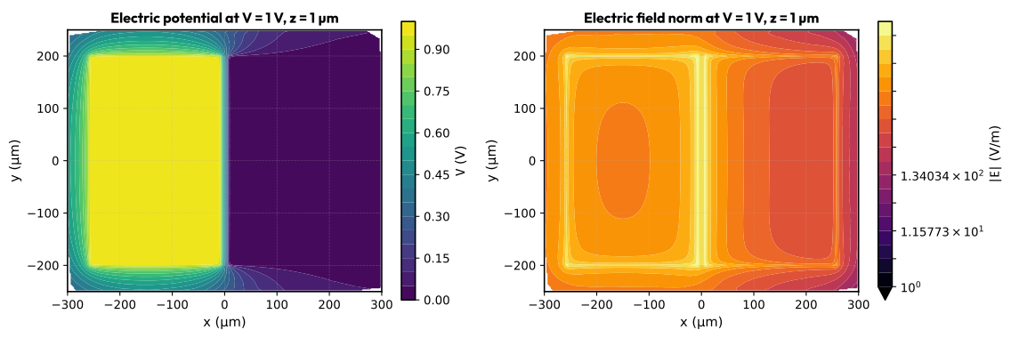
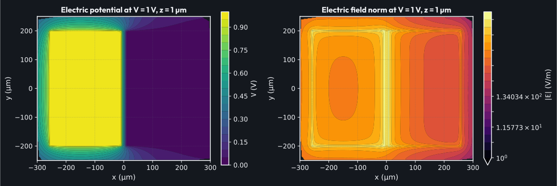
The potential holds across the driven pad and falls through the gap to the grounded pad; the field concentrates in that gap and at the pad edges, where the pad capacitance mainly lives.
Limitations and next steps#
The solve is electrostatic and the EM-only copy omits the SQUID loop and its leads, so \(C_{11}\) is a one-terminal capacitance to the grounded chip rather than the two-pad charging capacitance, and it is not a transmon eigenfrequency or \(f_{01}\). The finite zero-charge outer walls of the box act at any mesh, so the value is not a converged or validated device number. The natural next step is the full two-pad capacitance matrix feeding the QPDK Hamiltonian workflow (Dispersive Shift of a Transmon–Resonator System with scQubits).
References#
Alexandre Blais, Arne L. Grimsmo, S. M. Girvin, and Andreas Wallraff. Circuit quantum electrodynamics. Reviews of Modern Physics, 93(2):025005, May 2021. doi:10.1103/RevModPhys.93.025005.
Jens Koch, Terri M. Yu, Jay Gambetta, A. A. Houck, D. I. Schuster, J. Majer, Alexandre Blais, M. H. Devoret, S. M. Girvin, and R. J. Schoelkopf. Charge-insensitive qubit design derived from the Cooper pair box. Physical Review A, 76(4):042319, October 2007. doi:10.1103/PhysRevA.76.042319.
David M. Pozar. Microwave Engineering. John Wiley & Sons, Inc., 4 edition, 2012. ISBN 978-0-470-63155-3.