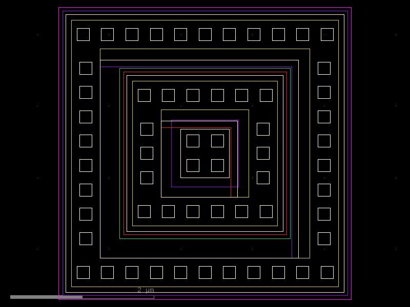
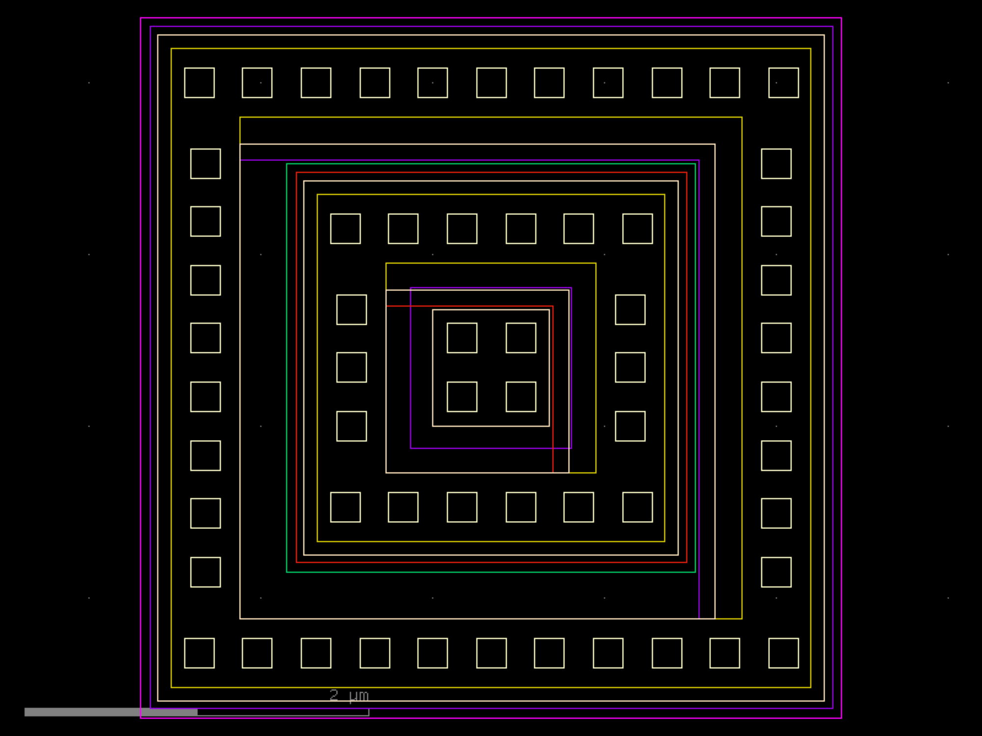
sky130.pcells.sky130_fd_pr__pnp_05v5#
- sky130.pcells.sky130_fd_pr__pnp_05v5(emitter_width=0.68, emitter_length=0.68, base_ring_width=0.4, np_spacing=0.27, sdm_enclosure=0.125, nwell_enclosure=0.18, li_enclosure=0.08)[source]#
Vertical PNP BJT for sky130 05V5 devices.
- Structure (inside-out):
Emitter: P+ diffusion (diffdrawing + psdmdrawing) rectangle
- Base: N-well (nwelldrawing) surrounding emitter, with N+ tap contacts
(tapdrawing + nsdmdrawing ring) for base access
Collector: P-substrate (accessed via outer P+ guard ring, tapdrawing + psdmdrawing)
Licon contacts on emitter and base/collector rings, Li1 pads
- Ports:
EMITTER, BASE, COLLECTOR on li1drawing layer.
- Parameters:
emitter_width (float) – Width of the emitter diffusion rectangle in um.
emitter_length (float) – Length of the emitter diffusion rectangle in um.
base_ring_width (float) – Width of the N+ base contact ring in um.
np_spacing (float) – Spacing between emitter edge and base ring in um.
sdm_enclosure (float) – Enclosure of SDM layers over diffusion in um.
nwell_enclosure (float) – Enclosure of nwell beyond the base contact ring in um.
li_enclosure (float) – Enclosure of li1 over licon contacts in um.
- Return type:
Component
import sky130

c = sky130.pcells.sky130_fd_pr__pnp_05v5()
c.plot()
(
Source code,png,hires.png,pdf)