Romero-García Visible SiN 1×4 MMI with GDSFactory FDTD
Split visible light into four outputs using a 100 nm silicon nitride multimode-interference device centered at 660 nm.
You will: build the component, configure the physical stack and 30 nm grid, preview the domain, and inspect transmission and a field monitor.
Requirements: GDSFactory+ cloud simulation access.
Reference run: 30 nm cells · 307,862,880 total allocated cells, including PML and padding.
Original paper
S. Romero-García et al., “Silicon nitride CMOS-compatible platform for integrated photonics applications at visible wavelengths,” Optics Express 21, 14036–14046 (2013). Read the paper · DOI 10.1364/OE.21.014036.
1. Build the component
All geometry below is in micrometers. The model includes fixed 200 nm straight leads at its modal ports.
import math

import gdsfactory as gf
import matplotlib.pyplot as plt
import numpy as np
from gdsfactory.technology import LayerLevel, LayerStack, LogicalLayer

from gsim import fdtd

gf.gpdk.PDK.activate()


def level(layer, material, zmin, thickness):
    return LayerLevel(
        layer=LogicalLayer(layer=layer),
        material=material,
        zmin=zmin,
        thickness=thickness,
        mesh_order=1,
        sidewall_angle=0,
    )
def extend_ports(component, length_um):
    """Append straight access guides and move each existing optical port."""
    ports = list(component.ports)
    component.ports.clear()
    for port in ports:
        angle = math.radians(port.orientation)
        normal = np.round([math.cos(angle), math.sin(angle)], 12)
        tangent = np.array([-normal[1], normal[0]])
        start = np.asarray(port.center)
        # GDS polygons are quantized to 1 nm; ports must share that face.
        end = np.round(start + length_um * normal, 3)
        half_width = port.width / 2
        component.add_polygon(
            [
                start - half_width * tangent,
                end - half_width * tangent,
                end + half_width * tangent,
                start + half_width * tangent,
            ],
            layer=port.layer,
        )
        component.add_port(
            name=port.name,
            center=tuple(end),
            width=port.width,
            orientation=port.orientation,
            layer=port.layer,
        )
component = gf.Component()
body_length_um, body_width_um, taper_length_um = 57.3, 9.7, 10
routing_width_um, aperture_width_um, output_pitch_um = 0.7, 1.5, 2.5
x0, x1 = taper_length_um, taper_length_um + body_length_um
component.add_polygon(
    [
        (x0, -body_width_um / 2),
        (x1, -body_width_um / 2),
        (x1, body_width_um / 2),
        (x0, body_width_um / 2),
    ],
    layer=(1, 0),
)
component.add_polygon(
    [
        (0, -routing_width_um / 2),
        (x0, -aperture_width_um / 2),
        (x0, aperture_width_um / 2),
        (0, routing_width_um / 2),
    ],
    layer=(1, 0),
)
component.add_port(
    name="o1", center=(0, 0), width=routing_width_um, orientation=180, layer=(1, 0)
)
for index, center_y in enumerate(output_pitch_um * np.array([-1.5, -0.5, 0.5, 1.5])):
    component.add_polygon(
        [
            (x1, center_y - aperture_width_um / 2),
            (x1 + taper_length_um, center_y - routing_width_um / 2),
            (x1 + taper_length_um, center_y + routing_width_um / 2),
            (x1, center_y + aperture_width_um / 2),
        ],
        layer=(1, 0),
    )
    component.add_port(
        name=f"o{index + 2}",
        center=(x1 + taper_length_um, float(center_y)),
        width=routing_width_um,
        orientation=0,
        layer=(1, 0),
    )
layers = {"core": level((1, 0), "SiN", 0, 0.1)}

extend_ports(component, 0.2)
2. Configure the simulation
Use explicit layer thicknesses and frozen source-center indices to reproduce the saved result. The 1.28 µm target PML is rounded up to whole cells. Materials are nondispersive over the sweep.
pdk = gf.Pdk(name="fdtd_romero_visible_mmi", layer_stack=LayerStack(layers=layers))
simulation = fdtd.Simulation(pdk=pdk)
simulation.geometry(component)
simulation.materials(background="SiO2", overrides={"SiN": 1.87, "SiO2": 1.45})
simulation.source(port="o1", wavelength_um=0.66, wavelength_span_um=0.1)
simulation.solver(cell_size_nm=30, max_wall_seconds=1800)
simulation.domain(
    pml_cells=43,
    x_bounds=((-0.2), (77.5)),
    y_bounds=((-5.8500000000000005), (5.8500000000000005)),
    z_bounds=((-1.88), (1.33)),
)

lower, upper = np.array(
    [[-0.2, -5.8500000000000005, -1.88], [77.5, 5.8500000000000005, 1.33]]
)
simulation.monitors.add_plane(
    "overview_xy",
    center_um=((lower[0] + upper[0]) / 2, (lower[1] + upper[1]) / 2, 0.05),
    size_um=(upper[0] - lower[0] - 0.24, upper[1] - lower[1] - 0.24, 0),
    normal="+z",
    flux=False,
    wavelengths_um=[0.66],
    heatmap=fdtd.Heatmap(quantity="intensity", wavelengths_um=[0.66]),
)
PlaneMonitor(name='overview_xy', center_um=(38.65, 0.0, 0.05), size_um=(77.46000000000001, 11.46, 0.0), normal='+z', flux=False, wavelengths_um=[0.66], heatmap=Heatmap(quantity='intensity', wavelengths_um=[0.66]), fiber_mode=None, fields=None)
3. Inspect the simulation
Use the built-in 2D views to inspect the core, ports, monitor and PML. The top view passes through the core; the side view shows the vertical stack.
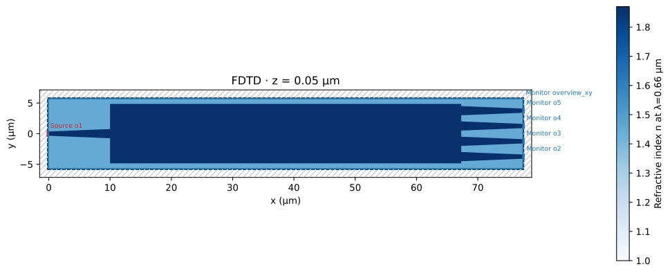
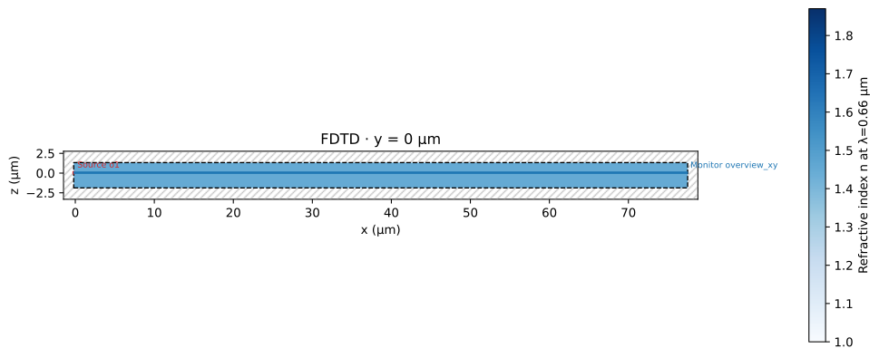
Rotate and zoom the built-in 3D viewer to inspect the complete simulation geometry.
4. Run the simulation
Reuse a matching result when it is available in the cloud cache.
print(f"Total allocated cells: {result.grid['total_cells']:,}")
print(f"Solver time: {result.timing['run_seconds']:.1f} s")
Total allocated cells: 307,862,880
Solver time: 433.5 s
5. Inspect transmission
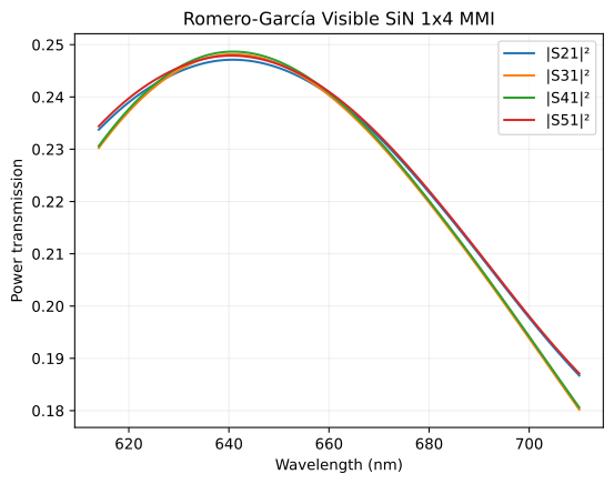
Plot incident-power-normalized modal transmission. Invalid source-band samples remain masked. Default Matplotlib figure size and fonts are used.
fig, ax = plt.subplots()
for port in ["o2", "o3", "o4", "o5"]:
    trace = result.s_parameters[port, "o1"]
    power = np.where(trace.valid, np.abs(trace.values) ** 2, np.nan)
    ax.plot(result.wavelength_um * 1000, power, label=f"|S{port[1:]}1|²")
ax.set(
    xlabel="Wavelength (nm)",
    ylabel="Power transmission",
    title="Romero-García Visible SiN 1x4 MMI",
)
ax.grid(alpha=0.2)
ax.legend()
plt.show()
6. Inspect the top-view field
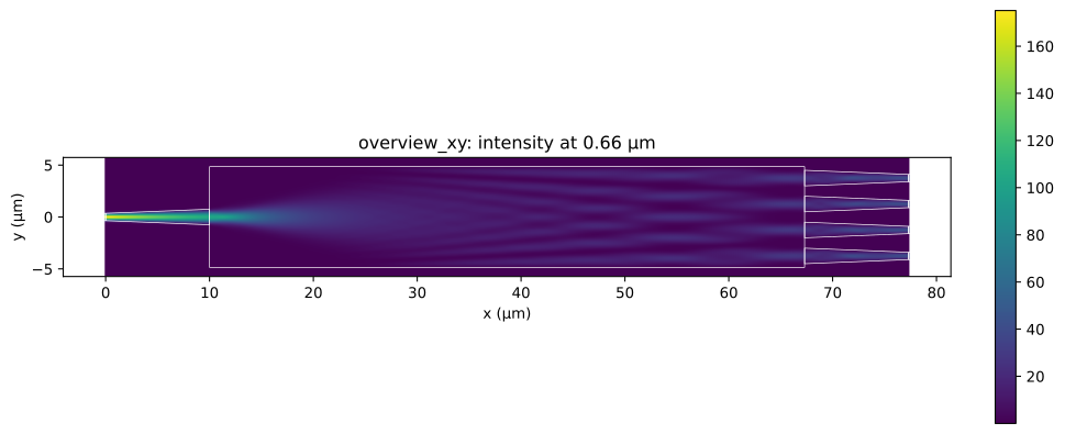
Overlay the silicon or silicon-nitride layout on the source-center intensity monitor. The x/y axes use equal aspect.
monitor = result.monitors["overview_xy"]
fig, ax = plt.subplots(figsize=(10, 4), layout="constrained")
monitor.plot_heatmap(
    wavelength_um=simulation.source.wavelength_um,
    quantity="intensity",
    ax=ax,
    cmap="viridis",
)
for points in component.get_polygons_points(by="tuple")[(1, 0)]:
    outline = np.vstack([points, points[0]])
    ax.plot(outline[:, 0], outline[:, 1], color="white", linewidth=0.5)
ax.set_aspect("equal", adjustable="box")
plt.show()
Model scope
The 57.3 × 9.7 µm body uses nominal 10 µm access tapers and constant published indices. The model retains 1.88 µm lower and 1.23 µm upper oxide clearance; remote substrate and air interfaces are omitted. The paper provides efficiency versus device length at 660 nm, not individual output wavelength spectra.
The saved result reached its finite-time stopping condition. That is separate from spatial mesh convergence. The reference campaign enforced a 30-minute wall-time budget.