

Palace Simulation of a Through-Silicon-Via CPW Transition#
This notebook takes a coplanar waveguide (CPW) from the front of a chip to its back through superconducting through-silicon vias (TSVs), models the transition in 3-D with gsim and Palace, and sets up the loop that tunes the taper and via placement for a 50 Ω match.
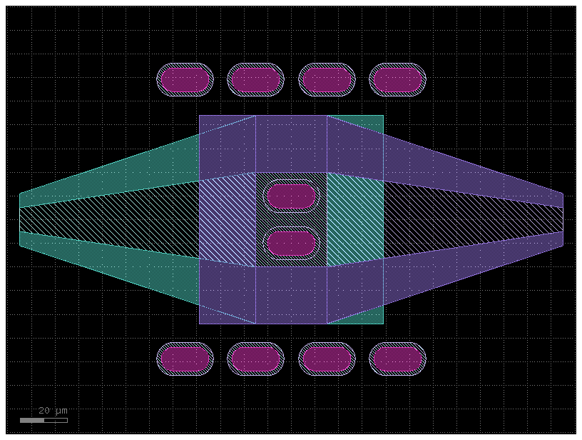
The design follows the side A to side B transition of [MYR+21]: 10 × 20 µm slot-shaped vias etched through the silicon, a CPW that tapers up to a pad large enough to land two signal TSVs in parallel, and a ring of ground TSVs stitching the front and back ground planes around it. A single narrow via is a large impedance discontinuity; the parallel signal vias, the pad and the ground ring together keep the reflection small.
        flowchart TB
    A["Analytical seed<br>(conductor-backed CPW)"]
    B["TSV transition layout<br>(qpdk cells)"]
    C["FEM regions<br>(front metal, back metal, TSVs)"]
    D["Double-sided layer stack"]
    E["Mesh and driven solve"]
    F["Optimise taper and vias<br>(minimise |S11|)"]
    A --> B --> C --> D --> E --> F
    F -->|next geometry| B
Required extras
This notebook needs the models extra:
uv add "qpdk[models]"
# or, from a checkout of this repository:
uv sync --extra models
# or with pip:
pip install "qpdk[models]"
The simulation cells additionally need the Palace solver itself, which is external to qpdk. The cells that invoke it are fenced behind environment variables (see Running Palace), so everything up to and including the mesh runs anywhere.
See the extras reference for what each extra installs.
Note
The saved Palace seed response is embedded below. The optimiser is optional because each evaluation needs another 3-D solve.
The via and the transition#
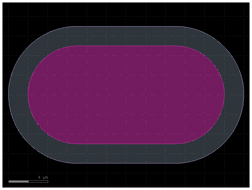
tsv() draws one slot-shaped via (a stadium, 10 µm wide and
20 µm long by default) with landing pads on both metal levels: M1 on the
front and MB, the new backside metal, on the back.
tsv_transition_double_sided() builds the full transition
out of it. Backside geometry is drawn in the front-side frame, as if looking
through the chip, so the two faces line up in the layout view.
via = tsv()
via.plot()
transition = tsv_transition_double_sided()
transition.plot()
Conductor-backed CPW: the analytical seed#
Metallising the back of the chip turns every CPW on the front into a
conductor-backed CPW (CBCPW): the backside ground sits one substrate
thickness \(h\) below the signal line and adds a parallel-plate path that
lowers \(Z_0\). cbcpw_parameters() implements the
conformal-mapping result [Sim01];
cpw_parameters(..., conductor_backed=True) switches the qpdk CPW models to
it. For the standard 10/6 µm line on 200 µm silicon the correction is small,
but it grows with the line’s lateral size, so it matters for the wide pad
the TSVs land on.
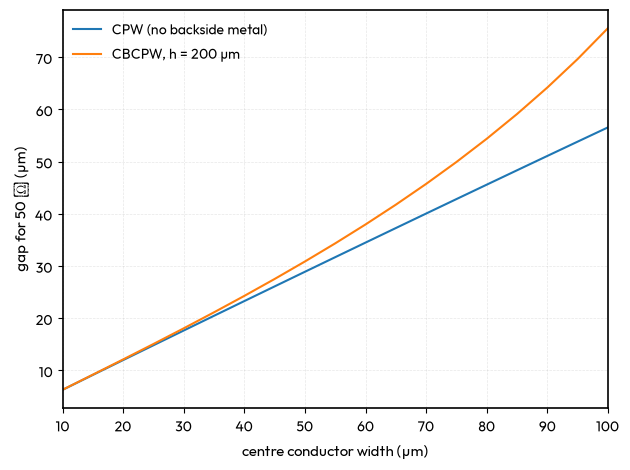
The seed geometry picks, for each pad width, the gap that gives 50 Ω as a CBCPW on the 200 µm substrate of the paper.
SUBSTRATE_THICKNESS = 200.0  # µm, the TSV depth
METAL_THICKNESS = 0.2  # µm
Z_TARGET = 50.0  # Ω
EP_R = material_properties["Si"]["relative_permittivity"]


def cbcpw_z0(width: float, gap: float, h: float = SUBSTRATE_THICKNESS) -> float:
    """Return the conductor-backed CPW impedance for µm dimensions."""
    _, z0 = cbcpw_parameters(
        width * 1e-6, gap * 1e-6, h * 1e-6, METAL_THICKNESS * 1e-6, EP_R
    )
    return float(z0)


def gap_for_z0(width: float, z0: float = Z_TARGET) -> float:
    """Return the CBCPW gap in µm that gives ``z0`` for a given width."""
    return brentq(lambda gap: cbcpw_z0(width, gap) - z0, 0.5, 20 * width)


widths = np.linspace(10.0, 100.0, 19)
gaps_backed = np.array([gap_for_z0(w) for w in widths])
gaps_free = np.array([
    brentq(lambda g, w=w: float(cpw_parameters(w, g)[1]) - Z_TARGET, 0.5, 20 * w)
    for w in widths
])

_, ax = plt.subplots()
ax.plot(widths, gaps_free, label="CPW (no backside metal)")
ax.plot(widths, gaps_backed, label=f"CBCPW, h = {SUBSTRATE_THICKNESS:.0f} µm")
ax.set_xlabel("centre conductor width (µm)")
ax.set_ylabel("gap for 50 Ω (µm)")
ax.legend()
plt.show()

seed_pad_width = 40.0
seed_pad_gap = gap_for_z0(seed_pad_width)
logger.info(
    f"lead 10/6 µm: {cbcpw_z0(10.0, 6.0):.2f} Ω backed,"
    f" {float(cpw_parameters(10.0, 6.0)[1]):.2f} Ω unbacked"
)
logger.info(f"seed pad: width {seed_pad_width:.0f} µm, gap {seed_pad_gap:.2f} µm")
findfont: Failed to find font weight bold, now using 400.
/Users/nikosavola/.worktrees/quantum-rf-pdk/palace-new/.venv/lib/python3.12/site-packages/IPython/core/pylabtools.py:170: UserWarning: Glyph 937 (\N{GREEK CAPITAL LETTER OMEGA}) missing from font(s) Outfit.
  fig.canvas.print_figure(bytes_io, **kw)
2026-09-29 02:33:36.042 | INFO | __main__:<module>:37 - lead 10/6 µm: 49.27 Ω backed, 49.31 Ω unbacked
2026-09-29 02:33:36.042 | INFO | __main__:<module>:41 - seed pad: width 40 µm, gap 24.29 µm
The two curves separate as the line widens: at 100 µm the backside metal calls for a visibly wider gap. The analytic model says nothing about the vias themselves, which is what the 3-D model is for.
Simulation layout#
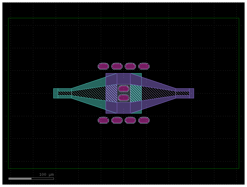
The simulation wraps the transition in three things:
Straight CPW leads on both faces. Palace’s lumped CPW port must sit on a uniform section: a port rectangle placed on the taper is no longer rectangular and fails gsim’s port check.
Etch stubs past each port, which end the signal line so the port drives it as an open-ended feed, as in Palace Eigenmode Simulation of a Transmon with a Readout Resonator.
A
SIM_AREArectangle 100 µm around the device, bounding the domain on both faces. The ground planes run to its edge.
sim_component takes the transition parameters, so the optimiser below
rebuilds the same wrapper around each candidate.
LEAD_LENGTH = 30.0  # µm
STUB_LENGTH = 10.0  # µm


@gf.cell
def sim_component(**params: Any) -> gf.Component:
    """TSV transition with CPW leads, etch stubs and a simulation area."""
    c = gf.Component()
    dut = c << tsv_transition_double_sided(**params)
    front = c << straight(length=LEAD_LENGTH, cross_section="cpw")
    front.connect("o2", dut.ports["o1"])
    back = c << straight(length=LEAD_LENGTH, cross_section="cpw_backside")
    back.connect("o1", dut.ports["o2"])
    c.add_port("o1", port=front.ports["o1"])
    c.add_port("o2", port=back.ports["o2"])
    for port, etch, sign in (
        (c.ports["o1"], LAYER.M1_ETCH, -1),
        (c.ports["o2"], LAYER.MB_ETCH, 1),
    ):
        half = port.width / 2 + 6.0  # signal plus the 6 µm gaps
        x0, x1 = sorted((port.x, port.x + sign * STUB_LENGTH))
        c.kdb_cell.shapes(gf.get_layer(etch)).insert(kdb.DBox(x0, -half, x1, half))
    c.kdb_cell.shapes(gf.get_layer(LAYER.SIM_AREA)).insert(c.bbox().enlarged(100, 100))
    return c


seed_params = {"pad_width": seed_pad_width, "pad_gap": round(seed_pad_gap, 2)}
layout_c = sim_component(**seed_params)
logger.info(f"simulation area: {layout_c.bbox()}")
layout_c.plot()
2026-09-29 02:33:36.058 | INFO | __main__:<module>:29 - simulation area: (-255,-166.29;255,166.29)
From etch layers to FEM regions#
to_tsv_regions() applies the subtractive convention
on both metal levels (conductor is SIM_AREA - ETCH + DRAW, matching
LAYER_STACK_BACKSIDE) and copies the TSVs to their own
region. The checks below are the circuit topology made visible: each face
splits into a ground plane and the signal line, and every via lands on
metal on both faces, so the ground vias really tie the two ground
planes together and the signal vias really carry the line through.
regions = to_tsv_regions(layout_c)
rlayout = regions.kdb_cell.layout()


def region(name: str) -> kdb.Region:
    """Return the merged region of one TSV FEM layer."""
    return kdb.Region(
        regions.kdb_cell.begin_shapes_rec(rlayout.layer(*TSV_FEM_LAYERS[name]))
    ).merged()


for name, (lnum, ldt) in TSV_FEM_LAYERS.items():
    logger.info(
        f"{name:>14} ({lnum},{ldt}): {len(region(name))} polygons,"
        f" {region(name).area() * 1e-6:.0f} µm²"
    )
m1, mb, vias = region("M1"), region("MB"), region("TSV")
assert len(m1) == 2, "front metal should be ground plane + signal line"
assert len(mb) == 2, "back metal should be ground plane + signal line"
assert (vias - m1).is_empty(), "a TSV does not land on front-side metal"
assert (vias - mb).is_empty(), "a TSV does not land on backside metal"
2026-09-29 02:33:36.139 | INFO | __main__:<module>:13 - VACUUM_BOTTOM (108,0): 1 polygons, 169616 µm²
2026-09-29 02:33:36.139 | INFO | __main__:<module>:13 - MB (109,0): 2 polygons, 162398 µm²
2026-09-29 02:33:36.139 | INFO | __main__:<module>:13 - SUBSTRATE (110,0): 1 polygons, 169616 µm²
2026-09-29 02:33:36.140 | INFO | __main__:<module>:13 - TSV (111,0): 10 polygons, 1784 µm²
2026-09-29 02:33:36.140 | INFO | __main__:<module>:13 - M1 (112,0): 2 polygons, 162398 µm²
2026-09-29 02:33:36.140 | INFO | __main__:<module>:13 - VACUUM (113,0): 1 polygons, 169616 µm²
Layer stack and driven setup#
tsv_stack() puts the front metal at \(z=0\) and the
backside metal at \(z=-h\), both as zero-thickness perfect conductors, with
air above and below the chip. The TSVs are “via” layers spanning the full
substrate. They need a material with a conductivity, without which gsim
demotes each via to a 2-D sheet at its base and the two faces no longer
connect. The model fills the vias solid, while the paper’s vias are TiN
liners around a hollow core; at microwave frequencies the current flows on
the via wall either way, so the solid via is a good approximation of the
field problem.
One CPW port sits on each face. The driven solve sweeps 1 to 12 GHz with Palace’s adaptive frequency sampling.
from gsim.palace import DrivenSim

from qpdk.simulation.palace_run import verify_port_connectivity

F_MIN, F_MAX = 1e9, 12e9  # Hz


def build_simulation(
    params: dict[str, float],
    sim_dir: Path,
    *,
    preset: Literal["coarse", "default", "fine"] = "coarse",
) -> DrivenSim:
    """Build, mesh and write a driven simulation of one transition geometry.

    Returns:
        The configured simulation, ready for a Palace solve in ``sim_dir``.
    """
    sim = DrivenSim()
    sim.set_geometry(to_tsv_regions(sim_component(**params)))
    sim.set_stack(
        tsv_stack(substrate_thickness=SUBSTRATE_THICKNESS, vacuum_thickness=300.0)
    )
    sim.set_numerical(order=1, solver_type="MUMPS")
    sim.add_cpw_port("o1", layer="M1", s_width=10.0, gap_width=6.0, length=5.0)
    sim.add_cpw_port("o2", layer="MB", s_width=10.0, gap_width=6.0, length=5.0)
    sim.set_driven(
        fmin=F_MIN,
        fmax=F_MAX,
        num_points=17,
        adaptive_tol=3e-3,
        reference_impedance=Z_TARGET,
    )
    sim.set_output_dir(sim_dir)
    sim.mesh(preset=preset, refined_mesh_size=2.0, auto_size=False, verbose=False)
    sim.write_config()
    config_path = sim_dir / "config.json"
    config = json.loads(config_path.read_text())
    config["Solver"]["Linear"]["MaxIts"] = 10
    config["Solver"]["Linear"]["ColumnOrdering"] = "ParMETIS"
    config_path.write_text(json.dumps(config, indent=2) + "\n")
    verify_port_connectivity(sim_dir)
    return sim


SIM_DIR = Path("./sim_palace_tsv")
sim = build_simulation(seed_params, SIM_DIR)
pyvirtualdisplay not available; continuing without Xvfb
Info    : Reading 'sim_palace_tsv/palace.msh'...
Info    : 113092 nodes
Info    : [  0%] Reading nodes
Info    : [ 10%] Reading nodes
Info    : [ 20%] Reading nodes
Info    : [ 30%] Reading nodes
Info    : [ 40%] Reading nodes
Info    : [ 50%] Reading nodes
Info    : [ 60%] Reading nodes
Info    : [ 70%] Reading nodes
Info    : [ 80%] Reading nodes
Info    : [ 90%] Reading nodes

Info    : 746979 elements
Info    : [  0%] Reading elements
Info    : [ 10%] Reading elements
Info    : [ 20%] Reading elements
Info    : [ 30%] Reading elements
Info    : [ 40%] Reading elements
Info    : [ 50%] Reading elements
Info    : [ 60%] Reading elements
Info    : [ 70%] Reading elements
Info    : [ 80%] Reading elements
Info    : [ 90%] Reading elements

Info    : Done reading 'sim_palace_tsv/palace.msh'
Info    : Reading 'sim_palace_tsv/palace.msh'...
Info    : 113092 nodes
Info    : [  0%] Reading nodes
Info    : [ 10%] Reading nodes
Info    : [ 20%] Reading nodes
Info    : [ 30%] Reading nodes
Info    : [ 40%] Reading nodes
Info    : [ 50%] Reading nodes
Info    : [ 60%] Reading nodes
Info    : [ 70%] Reading nodes
Info    : [ 80%] Reading nodes
Info    : [ 90%] Reading nodes

Info    : 746979 elements
Info    : [  0%] Reading elements
Info    : [ 10%] Reading elements
Info    : [ 20%] Reading elements
Info    : [ 30%] Reading elements
Info    : [ 40%] Reading elements
Info    : [ 50%] Reading elements
Info    : [ 60%] Reading elements
Info    : [ 70%] Reading elements
Info    : [ 80%] Reading elements
Info    : [ 90%] Reading elements

Info    : Done reading 'sim_palace_tsv/palace.msh'
Info    : Reading 'sim_palace_tsv/palace.msh'...
Info    : 113092 nodes
Info    : [  0%] Reading nodes
Info    : [ 10%] Reading nodes
Info    : [ 20%] Reading nodes
Info    : [ 30%] Reading nodes
Info    : [ 40%] Reading nodes
Info    : [ 50%] Reading nodes
Info    : [ 60%] Reading nodes
Info    : [ 70%] Reading nodes
Info    : [ 80%] Reading nodes
Info    : [ 90%] Reading nodes

Info    : 746979 elements
Info    : [  0%] Reading elements
Info    : [ 10%] Reading elements
Info    : [ 20%] Reading elements
Info    : [ 30%] Reading elements
Info    : [ 40%] Reading elements
Info    : [ 50%] Reading elements
Info    : [ 60%] Reading elements
Info    : [ 70%] Reading elements
Info    : [ 80%] Reading elements
Info    : [ 90%] Reading elements

Info    : Done reading 'sim_palace_tsv/palace.msh'
Info    : Reading 'sim_palace_tsv/palace.msh'...
Info    : 113092 nodes
Info    : [  0%] Reading nodes
Info    : [ 10%] Reading nodes
Info    : [ 20%] Reading nodes
Info    : [ 30%] Reading nodes
Info    : [ 40%] Reading nodes
Info    : [ 50%] Reading nodes
Info    : [ 60%] Reading nodes
Info    : [ 70%] Reading nodes
Info    : [ 80%] Reading nodes
Info    : [ 90%] Reading nodes

Info    : 746979 elements
Info    : [  0%] Reading elements
Info    : [ 10%] Reading elements
Info    : [ 20%] Reading elements
Info    : [ 30%] Reading elements
Info    : [ 40%] Reading elements
Info    : [ 50%] Reading elements
Info    : [ 60%] Reading elements
Info    : [ 70%] Reading elements
Info    : [ 80%] Reading elements
Info    : [ 90%] Reading elements

Info    : Done reading 'sim_palace_tsv/palace.msh'
Info    : Reading 'sim_palace_tsv/palace.msh'...
Info    : 113092 nodes
Info    : [  0%] Reading nodes
Info    : [ 10%] Reading nodes
Info    : [ 20%] Reading nodes
Info    : [ 30%] Reading nodes
Info    : [ 40%] Reading nodes
Info    : [ 50%] Reading nodes
Info    : [ 60%] Reading nodes
Info    : [ 70%] Reading nodes
Info    : [ 80%] Reading nodes
Info    : [ 90%] Reading nodes

Info    : 746979 elements
Info    : [  0%] Reading elements
Info    : [ 10%] Reading elements
Info    : [ 20%] Reading elements
Info    : [ 30%] Reading elements
Info    : [ 40%] Reading elements
Info    : [ 50%] Reading elements
Info    : [ 60%] Reading elements
Info    : [ 70%] Reading elements
Info    : [ 80%] Reading elements
Info    : [ 90%] Reading elements

Info    : Done reading 'sim_palace_tsv/palace.msh'
Mesh checks#
The volumes should span the chip and the air on both sides, and the two PEC sheets should sit at \(z=0\) and \(z=-h\). The port check above has already confirmed that both CPW ports share mesh nodes with metal.
Info    : Reading 'sim_palace_tsv/palace.msh'...
Info    : 113092 nodes
Info    : [  0%] Reading nodes
Info    : [ 10%] Reading nodes
Info    : [ 20%] Reading nodes
Info    : [ 30%] Reading nodes
Info    : [ 40%] Reading nodes
Info    : [ 50%] Reading nodes
Info    : [ 60%] Reading nodes
Info    : [ 70%] Reading nodes
Info    : [ 80%] Reading nodes
Info    : [ 90%] Reading nodes

Info    : 746979 elements
Info    : [  0%] Reading elements
Info    : [ 10%] Reading elements
Info    : [ 20%] Reading elements
Info    : [ 30%] Reading elements
Info    : [ 40%] Reading elements
Info    : [ 50%] Reading elements
Info    : [ 60%] Reading elements
Info    : [ 70%] Reading elements
Info    : [ 80%] Reading elements
Info    : [ 90%] Reading elements
2026-09-29 02:35:05.183 | INFO | __main__:<module>:9 - volume VACUUM_BOTTOM: z [-500, -200] µm
2026-09-29 02:35:05.187 | INFO | __main__:<module>:9 - volume SUBSTRATE: z [-200, 0] µm
2026-09-29 02:35:05.187 | INFO | __main__:<module>:9 - volume TSV: z [-200, 0] µm
2026-09-29 02:35:05.188 | INFO | __main__:<module>:9 - volume VACUUM: z [-0, 300] µm
2026-09-29 02:35:05.188 | INFO | __main__:<module>:20 - surface MB_pec: z = -200 µm
2026-09-29 02:35:05.188 | INFO | __main__:<module>:20 - surface M1_pec: z = -0 µm
Info : Done reading 'sim_palace_tsv/palace.msh'
Running Palace#
The solve needs the Palace binary: set QPDK_RUN_TSV_SOLVE=1 and either
put palace on PATH or point QPDK_PALACE_SIF at an Apptainer
image. solve() launches it with
QPDK_SOLVER_CORES MPI ranks, and gsim reads the S-parameters back.
\(|S_{11}|\) from the two-port S-matrix is the figure of merit; the reflection also gives the input impedance that the transition presents to the front-side 50 Ω line,
from gsim.palace import load_sparams

from qpdk.simulation.palace_run import solve

RUN_SOLVE = os.environ.get("QPDK_RUN_TSV_SOLVE") == "1"
RUN_OPTIMIZATION = os.environ.get("QPDK_RUN_TSV_OPTIMIZATION") == "1"
RANKS = int(os.environ.get("QPDK_SOLVER_CORES") or 8)
BAND = (4.0, 8.0)  # GHz, the units of Palace's port-S.csv


def plot_sparams(f: np.ndarray, s11: np.ndarray, s21: np.ndarray) -> None:
    """Plot the two-port response with frequency in GHz."""
    z_in = Z_TARGET * (1 + s11) / (1 - s11)
    fig, (ax_s, ax_z) = plt.subplots(1, 2, figsize=(10, 4))
    ax_s.plot(f, 20 * np.log10(np.abs(s11)), label="$|S_{11}|$")
    ax_s.plot(f, 20 * np.log10(np.abs(s21)), label="$|S_{21}|$")
    ax_s.axvspan(*BAND, alpha=0.1)
    ax_s.set(xlabel="frequency (GHz)", ylabel="dB")
    ax_s.legend()
    ax_z.plot(f, z_in.real, label=r"Re $Z_\text{in}$")
    ax_z.plot(f, z_in.imag, label=r"Im $Z_\text{in}$")
    ax_z.axhline(Z_TARGET, color="k", lw=0.5)
    ax_z.set(xlabel="frequency (GHz)", ylabel="Ω")
    ax_z.legend()
    plt.show()
    plt.close(fig)
Saved seed response#
Palace solved the seed geometry with first-order elements on a mesh refined
to 2 µm near the metal, using 17 frequency samples and a 0.3% adaptive
tolerance. The table is the first excitation of its port-S.csv. It is a
seed result; the optimisation loop below has not been run.
/Users/nikosavola/.worktrees/quantum-rf-pdk/palace-new/.venv/lib/python3.12/site-packages/IPython/core/pylabtools.py:170: UserWarning: Glyph 937 (\N{GREEK CAPITAL LETTER OMEGA}) missing from font(s) Outfit.
  fig.canvas.print_figure(bytes_io, **kw)
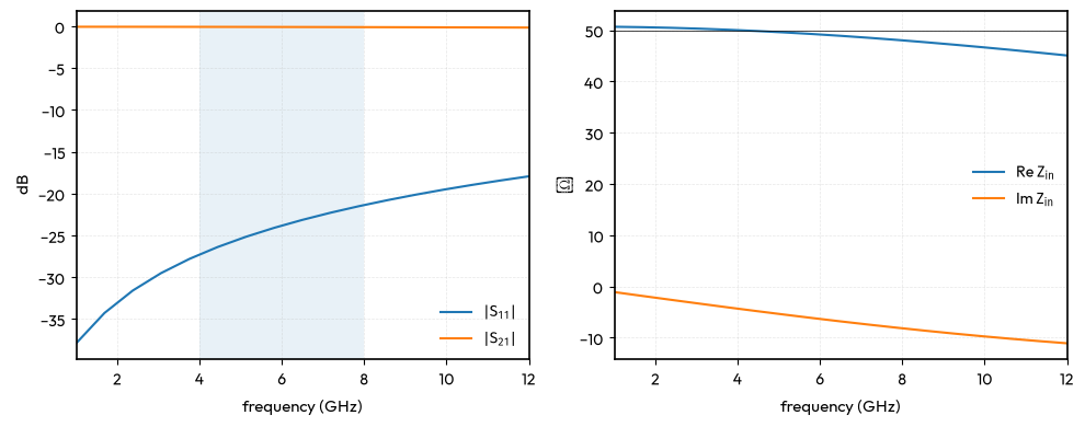
2026-09-29 02:35:05.282 | INFO | __main__:<module>:41 - worst sampled |S11| from 4 to 8 GHz: -21.5 dB
Optimising the transition for 50 Ω#
The paper tunes the transition shape to minimise reflections. The loop below does the same with Palace: each evaluation builds a geometry, meshes it, solves it, and scores it by the worst in-band reflection,
The free parameters are the ones the analytic model cannot fix: the taper length, the pad width, the spacing of the two signal vias and the distance of the ground-via ring from the pad edge. The pad gap is not a free parameter: it follows the pad width through the CBCPW seed, so the pad stays a 50 Ω line and the optimiser spends its evaluations on the vias. Nelder–Mead from the seed needs no gradients and tolerates the small mesh noise between neighbouring geometries; each evaluation is one independent Palace run, so the same objective drops into the Optuna/Slurm driver of Batched Layout Optimisation of a Transmon with Optuna for a wider search.
from scipy.optimize import minimize

PARAMETERS = {
    # name: (seed, lower bound, upper bound), µm
    "taper_length": (100.0, 30.0, 250.0),
    "pad_width": (seed_pad_width, 30.0, 80.0),
    "signal_via_pitch": (20.0, 14.0, 34.0),
    "ground_via_distance": (15.0, 8.0, 60.0),
}


def geometry(x: np.ndarray) -> dict[str, float]:
    """Map an optimiser vector to transition parameters, 50 Ω pad included."""
    params = {name: round(float(v), 2) for name, v in zip(PARAMETERS, x, strict=True)}
    params["taper_length_backside"] = params["taper_length"]
    params["pad_gap"] = round(gap_for_z0(params["pad_width"]), 2)
    return params


def objective(x: np.ndarray, run_root: Path = Path("./sim_palace_tsv_opt")) -> float:
    """Return the worst in-band |S11| in dB for one geometry."""
    params = geometry(x)
    sim_dir = run_root / "_".join(f"{v:g}" for v in params.values())
    try:
        build_simulation(params, sim_dir)
    except ValueError as err:  # geometry the cell rejects, e.g. vias off the pad
        logger.warning(f"{params}: {err}")
        return 0.0
    solve(sim_dir, ranks=RANKS)
    sp = load_sparams(sim_dir)
    f = np.asarray(sp.freq)
    in_band = (f >= BAND[0]) & (f <= BAND[1])
    cost = float(np.max(np.asarray(sp["o1", "o1"].db)[in_band]))
    logger.info(f"{params} -> max |S11| = {cost:.1f} dB")
    return cost


x0 = np.array([seed for seed, _, _ in PARAMETERS.values()])
bounds = [(lo, hi) for _, lo, hi in PARAMETERS.values()]
logger.info(f"seed geometry: {geometry(x0)}")

if RUN_OPTIMIZATION:
    result = minimize(
        objective,
        x0,
        method="Nelder-Mead",
        bounds=bounds,
        options={"maxfev": 40, "xatol": 1.0, "fatol": 0.5},
    )
    best = geometry(result.x)
    logger.info(f"best geometry: {best}, max |S11| = {result.fun:.1f} dB")
    best_dir = Path("./sim_palace_tsv_best")
    build_simulation(best, best_dir, preset="default")
    solve(best_dir, ranks=RANKS)
    best_sp = load_sparams(best_dir)
    plot_sparams(
        np.asarray(best_sp.freq),
        np.asarray(best_sp["o1", "o1"].complex),
        np.asarray(best_sp["o2", "o1"].complex),
    )
else:
    logger.info("QPDK_RUN_TSV_OPTIMIZATION is not set; skipping the optimisation.")
2026-09-29 02:35:05.287 | INFO | __main__:<module>:40 - seed geometry: {'taper_length': 100.0, 'pad_width': 40.0, 'signal_via_pitch': 20.0, 'ground_via_distance': 15.0, 'taper_length_backside': 100.0, 'pad_gap': 24.29}
2026-09-29 02:35:05.287 | INFO | __main__:<module>:62 - QPDK_RUN_TSV_OPTIMIZATION is not set; skipping the optimisation.
A rejected geometry scores 0 dB, a total reflection, so the optimiser
backs away from it instead of stopping. The best geometry is re-solved on
the finer default mesh preset before it is trusted: a match found on a
coarse mesh can partly be a mesh artefact.
Summary#
tsv()andtsv_transition_double_sided()draw the slot vias and the two-signal-via transition of [MYR+21] on the newMBbackside metal.The backside metal makes the CPWs conductor-backed;
cbcpw_parameters()and theconductor_backedswitch of the CPW models account for it and seed the pad geometry at 50 Ω.to_tsv_regions()andtsv_stack()produce a meshed, port-checked Palace model of the transition, and the objective above closes the loop on \(|S_{11}|\).
Natural next steps: model the TSV liner as a thin conductive shell rather than a solid via, and add the kinetic inductance of the thin TiN lining, which a PEC-and-conductor model leaves out.
References#
Justin L. Mallek, Donna-Ruth W. Yost, Danna Rosenberg, Jonilyn L. Yoder, Gregory Calusine, Matt Cook, Rabindra Das, Alexandra Day, Evan Golden, David K. Kim, Jeffery Knecht, Bethany M. Niedzielski, Mollie Schwartz, Arjan Sevi, Corey Stull, Wayne Woods, Andrew J. Kerman, and William D. Oliver. Fabrication of superconducting through-silicon vias. March 2021. doi:10.48550/arXiv.2103.08536.
Rainee Simons. Coplanar Waveguide Circuits, Components, and Systems. Number v. 165 in Wiley Series in Microwave and Optical Engineering. Wiley Interscience, New York, 2001. ISBN 978-0-471-46393-1. doi:10.1002/0471224758.