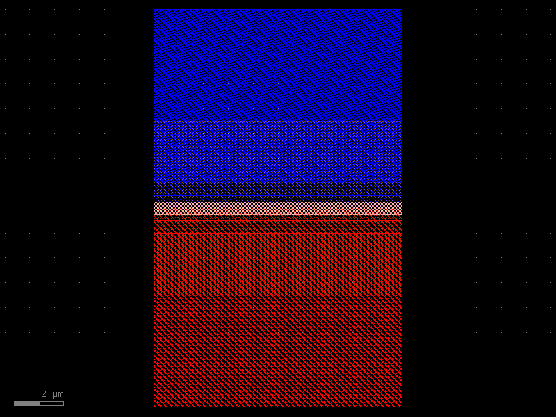
gdsfactory.cross_section.pn_ge_detector_si_contacts#
- gdsfactory.cross_section.pn_ge_detector_si_contacts(width_si=6.0, layer_si='WG', width_ge=3.0, layer_ge='GE', gap_low_doping=0.6, gap_medium_doping=0.9, gap_high_doping=1.1, width_doping=8.0, layer_p='P', layer_pp='PP', layer_ppp='PPP', layer_n='N', layer_np='NP', layer_npp='NPP', layer_via=None, width_via=1.0, layer_metal=None, port_names=('o1', 'o2'), cladding_layers=None, cladding_offsets=None, cladding_simplify=None, **kwargs)[source]#
Linear Ge detector cross section based on a lateral p(i)n junction.
It has silicon contacts (no contact on the Ge). The contacts need to be created in the component generating function (they can’t be created here).
See Chen et al., “High-Responsivity Low-Voltage 28-Gb/s Ge p-i-n Photodetector With Silicon Contacts”, Journal of Lightwave Technology 33(4), 2015.
Notice it is possible to have dopings going beyond the ridge waveguide. This is fine, and it is to account for the presence of the contacts. Such contacts can be subwavelength or not.
- Parameters:
width_si (float) – width of the full etch si in um.
layer_si (tuple[int, int] | str | int | LayerEnum) – si ridge layer.
width_ge (float) – width of the ge in um.
layer_ge (tuple[int, int] | str | int | LayerEnum) – ge layer.
gap_low_doping (float) – from waveguide center to low doping.
gap_medium_doping (float) – from waveguide center to medium doping. None removes it.
gap_high_doping (float) – from center to high doping. None removes it.
width_doping (float) – distance from waveguide center to doping edge in um.
layer_p (tuple[int, int] | str | int | LayerEnum) – p doping layer.
layer_pp (tuple[int, int] | str | int | LayerEnum) – p+ doping layer.
layer_ppp (tuple[int, int] | str | int | LayerEnum) – p++ doping layer.
layer_n (tuple[int, int] | str | int | LayerEnum) – n doping layer.
layer_np (tuple[int, int] | str | int | LayerEnum) – n+ doping layer.
layer_npp (tuple[int, int] | str | int | LayerEnum) – n++ doping layer.
layer_via (tuple[int, int] | str | int | LayerEnum | None) – via layer.
width_via (float) – via width in um.
layer_metal (tuple[int, int] | str | int | LayerEnum | None) – metal layer.
port_names (tuple[str, str]) – for input and output (‘o1’, ‘o2’).
cladding_layers (Sequence[tuple[int, int]] | None) – list of layers to extrude.
cladding_offsets (Sequence[float] | None) – list of offset from main Section edge.
cladding_simplify (Sequence[float] | None) – Optional Tolerance value for the simplification algorithm. All points that can be removed without changing the resulting. polygon by more than the value listed here will be removed.
kwargs (Any) – cross_section settings.
- Return type:
                           layer_si
                   |<------width_si---->|

                          layer_ge
                      |<--width_ge->|
                       ______________
                      |             |
                    __|_____________|___
                   |     |       |     |
                   |     |       |     |
            P      |     |       |     |         N                |
         width_p   |_____|_______|_____|           width_n        |
<----------------------->|       |<------------------------------>|
                             |<->|
                             gap_low_doping
                             |         |        N+                |
                             |         |     width_np             |
                             |         |<------------------------>|
                             |<------->|
                             |     gap_medium_doping
                             |
                             |<---------------------------------->|
                                        width_doping
import gdsfactory as gf

xs = gf.cross_section.pn()
p = gf.path.straight()
c = p.extrude(xs)
c.plot()
(
Source code,png,hires.png,pdf)
